EP1391495B2 - Organisches elektrolumineszenzelement - Google Patents
Organisches elektrolumineszenzelement Download PDFInfo
- Publication number
- EP1391495B2 EP1391495B2 EP02724727.9A EP02724727A EP1391495B2 EP 1391495 B2 EP1391495 B2 EP 1391495B2 EP 02724727 A EP02724727 A EP 02724727A EP 1391495 B2 EP1391495 B2 EP 1391495B2
- Authority
- EP
- European Patent Office
- Prior art keywords
- light emitting
- organic
- layer
- heavy metal
- organometallic complex
- Prior art date
- Legal status (The legal status is an assumption and is not a legal conclusion. Google has not performed a legal analysis and makes no representation as to the accuracy of the status listed.)
- Expired - Lifetime
Links
Classifications
-
- C—CHEMISTRY; METALLURGY
- C09—DYES; PAINTS; POLISHES; NATURAL RESINS; ADHESIVES; COMPOSITIONS NOT OTHERWISE PROVIDED FOR; APPLICATIONS OF MATERIALS NOT OTHERWISE PROVIDED FOR
- C09K—MATERIALS FOR MISCELLANEOUS APPLICATIONS, NOT PROVIDED FOR ELSEWHERE
- C09K11/00—Luminescent materials, e.g. electroluminescent or chemiluminescent
- C09K11/06—Luminescent materials, e.g. electroluminescent or chemiluminescent containing organic luminescent materials
-
- C—CHEMISTRY; METALLURGY
- C07—ORGANIC CHEMISTRY
- C07D—HETEROCYCLIC COMPOUNDS
- C07D213/00—Heterocyclic compounds containing six-membered rings, not condensed with other rings, with one nitrogen atom as the only ring hetero atom and three or more double bonds between ring members or between ring members and non-ring members
- C07D213/02—Heterocyclic compounds containing six-membered rings, not condensed with other rings, with one nitrogen atom as the only ring hetero atom and three or more double bonds between ring members or between ring members and non-ring members having three double bonds between ring members or between ring members and non-ring members
- C07D213/04—Heterocyclic compounds containing six-membered rings, not condensed with other rings, with one nitrogen atom as the only ring hetero atom and three or more double bonds between ring members or between ring members and non-ring members having three double bonds between ring members or between ring members and non-ring members having no bond between the ring nitrogen atom and a non-ring member or having only hydrogen or carbon atoms directly attached to the ring nitrogen atom
- C07D213/06—Heterocyclic compounds containing six-membered rings, not condensed with other rings, with one nitrogen atom as the only ring hetero atom and three or more double bonds between ring members or between ring members and non-ring members having three double bonds between ring members or between ring members and non-ring members having no bond between the ring nitrogen atom and a non-ring member or having only hydrogen or carbon atoms directly attached to the ring nitrogen atom containing only hydrogen and carbon atoms in addition to the ring nitrogen atom
- C07D213/16—Heterocyclic compounds containing six-membered rings, not condensed with other rings, with one nitrogen atom as the only ring hetero atom and three or more double bonds between ring members or between ring members and non-ring members having three double bonds between ring members or between ring members and non-ring members having no bond between the ring nitrogen atom and a non-ring member or having only hydrogen or carbon atoms directly attached to the ring nitrogen atom containing only hydrogen and carbon atoms in addition to the ring nitrogen atom containing only one pyridine ring
-
- H—ELECTRICITY
- H10—SEMICONDUCTOR DEVICES; ELECTRIC SOLID-STATE DEVICES NOT OTHERWISE PROVIDED FOR
- H10K—ORGANIC ELECTRIC SOLID-STATE DEVICES
- H10K50/00—Organic light-emitting devices
-
- H—ELECTRICITY
- H10—SEMICONDUCTOR DEVICES; ELECTRIC SOLID-STATE DEVICES NOT OTHERWISE PROVIDED FOR
- H10K—ORGANIC ELECTRIC SOLID-STATE DEVICES
- H10K50/00—Organic light-emitting devices
- H10K50/10—OLEDs or polymer light-emitting diodes [PLED]
- H10K50/11—OLEDs or polymer light-emitting diodes [PLED] characterised by the electroluminescent [EL] layers
-
- H—ELECTRICITY
- H10—SEMICONDUCTOR DEVICES; ELECTRIC SOLID-STATE DEVICES NOT OTHERWISE PROVIDED FOR
- H10K—ORGANIC ELECTRIC SOLID-STATE DEVICES
- H10K85/00—Organic materials used in the body or electrodes of devices covered by this subclass
- H10K85/30—Coordination compounds
- H10K85/321—Metal complexes comprising a group IIIA element, e.g. Tris (8-hydroxyquinoline) gallium [Gaq3]
- H10K85/324—Metal complexes comprising a group IIIA element, e.g. Tris (8-hydroxyquinoline) gallium [Gaq3] comprising aluminium, e.g. Alq3
-
- H—ELECTRICITY
- H10—SEMICONDUCTOR DEVICES; ELECTRIC SOLID-STATE DEVICES NOT OTHERWISE PROVIDED FOR
- H10K—ORGANIC ELECTRIC SOLID-STATE DEVICES
- H10K85/00—Organic materials used in the body or electrodes of devices covered by this subclass
- H10K85/30—Coordination compounds
- H10K85/341—Transition metal complexes, e.g. Ru(II)polypyridine complexes
-
- H—ELECTRICITY
- H10—SEMICONDUCTOR DEVICES; ELECTRIC SOLID-STATE DEVICES NOT OTHERWISE PROVIDED FOR
- H10K—ORGANIC ELECTRIC SOLID-STATE DEVICES
- H10K85/00—Organic materials used in the body or electrodes of devices covered by this subclass
- H10K85/30—Coordination compounds
- H10K85/341—Transition metal complexes, e.g. Ru(II)polypyridine complexes
- H10K85/342—Transition metal complexes, e.g. Ru(II)polypyridine complexes comprising iridium
-
- H—ELECTRICITY
- H10—SEMICONDUCTOR DEVICES; ELECTRIC SOLID-STATE DEVICES NOT OTHERWISE PROVIDED FOR
- H10K—ORGANIC ELECTRIC SOLID-STATE DEVICES
- H10K85/00—Organic materials used in the body or electrodes of devices covered by this subclass
- H10K85/60—Organic compounds having low molecular weight
- H10K85/631—Amine compounds having at least two aryl rest on at least one amine-nitrogen atom, e.g. triphenylamine
-
- H—ELECTRICITY
- H10—SEMICONDUCTOR DEVICES; ELECTRIC SOLID-STATE DEVICES NOT OTHERWISE PROVIDED FOR
- H10K—ORGANIC ELECTRIC SOLID-STATE DEVICES
- H10K85/00—Organic materials used in the body or electrodes of devices covered by this subclass
- H10K85/60—Organic compounds having low molecular weight
- H10K85/631—Amine compounds having at least two aryl rest on at least one amine-nitrogen atom, e.g. triphenylamine
- H10K85/633—Amine compounds having at least two aryl rest on at least one amine-nitrogen atom, e.g. triphenylamine comprising polycyclic condensed aromatic hydrocarbons as substituents on the nitrogen atom
-
- C—CHEMISTRY; METALLURGY
- C09—DYES; PAINTS; POLISHES; NATURAL RESINS; ADHESIVES; COMPOSITIONS NOT OTHERWISE PROVIDED FOR; APPLICATIONS OF MATERIALS NOT OTHERWISE PROVIDED FOR
- C09K—MATERIALS FOR MISCELLANEOUS APPLICATIONS, NOT PROVIDED FOR ELSEWHERE
- C09K2211/00—Chemical nature of organic luminescent or tenebrescent compounds
- C09K2211/10—Non-macromolecular compounds
- C09K2211/1003—Carbocyclic compounds
-
- C—CHEMISTRY; METALLURGY
- C09—DYES; PAINTS; POLISHES; NATURAL RESINS; ADHESIVES; COMPOSITIONS NOT OTHERWISE PROVIDED FOR; APPLICATIONS OF MATERIALS NOT OTHERWISE PROVIDED FOR
- C09K—MATERIALS FOR MISCELLANEOUS APPLICATIONS, NOT PROVIDED FOR ELSEWHERE
- C09K2211/00—Chemical nature of organic luminescent or tenebrescent compounds
- C09K2211/10—Non-macromolecular compounds
- C09K2211/1003—Carbocyclic compounds
- C09K2211/1007—Non-condensed systems
-
- C—CHEMISTRY; METALLURGY
- C09—DYES; PAINTS; POLISHES; NATURAL RESINS; ADHESIVES; COMPOSITIONS NOT OTHERWISE PROVIDED FOR; APPLICATIONS OF MATERIALS NOT OTHERWISE PROVIDED FOR
- C09K—MATERIALS FOR MISCELLANEOUS APPLICATIONS, NOT PROVIDED FOR ELSEWHERE
- C09K2211/00—Chemical nature of organic luminescent or tenebrescent compounds
- C09K2211/10—Non-macromolecular compounds
- C09K2211/1003—Carbocyclic compounds
- C09K2211/1011—Condensed systems
-
- C—CHEMISTRY; METALLURGY
- C09—DYES; PAINTS; POLISHES; NATURAL RESINS; ADHESIVES; COMPOSITIONS NOT OTHERWISE PROVIDED FOR; APPLICATIONS OF MATERIALS NOT OTHERWISE PROVIDED FOR
- C09K—MATERIALS FOR MISCELLANEOUS APPLICATIONS, NOT PROVIDED FOR ELSEWHERE
- C09K2211/00—Chemical nature of organic luminescent or tenebrescent compounds
- C09K2211/10—Non-macromolecular compounds
- C09K2211/1003—Carbocyclic compounds
- C09K2211/1014—Carbocyclic compounds bridged by heteroatoms, e.g. N, P, Si or B
-
- C—CHEMISTRY; METALLURGY
- C09—DYES; PAINTS; POLISHES; NATURAL RESINS; ADHESIVES; COMPOSITIONS NOT OTHERWISE PROVIDED FOR; APPLICATIONS OF MATERIALS NOT OTHERWISE PROVIDED FOR
- C09K—MATERIALS FOR MISCELLANEOUS APPLICATIONS, NOT PROVIDED FOR ELSEWHERE
- C09K2211/00—Chemical nature of organic luminescent or tenebrescent compounds
- C09K2211/18—Metal complexes
- C09K2211/185—Metal complexes of the platinum group, i.e. Os, Ir, Pt, Ru, Rh or Pd
-
- H—ELECTRICITY
- H10—SEMICONDUCTOR DEVICES; ELECTRIC SOLID-STATE DEVICES NOT OTHERWISE PROVIDED FOR
- H10K—ORGANIC ELECTRIC SOLID-STATE DEVICES
- H10K2102/00—Constructional details relating to the organic devices covered by this subclass
- H10K2102/10—Transparent electrodes, e.g. using graphene
- H10K2102/101—Transparent electrodes, e.g. using graphene comprising transparent conductive oxides [TCO]
- H10K2102/103—Transparent electrodes, e.g. using graphene comprising transparent conductive oxides [TCO] comprising indium oxides, e.g. ITO
-
- H—ELECTRICITY
- H10—SEMICONDUCTOR DEVICES; ELECTRIC SOLID-STATE DEVICES NOT OTHERWISE PROVIDED FOR
- H10K—ORGANIC ELECTRIC SOLID-STATE DEVICES
- H10K85/00—Organic materials used in the body or electrodes of devices covered by this subclass
- H10K85/30—Coordination compounds
- H10K85/341—Transition metal complexes, e.g. Ru(II)polypyridine complexes
- H10K85/344—Transition metal complexes, e.g. Ru(II)polypyridine complexes comprising ruthenium
Definitions
- the present invention relates to an organic electroluminescence device used as a planar light emitting member of wall televisions and a light source for a back light of displays, and more particularly, to an organic electroluminescence device exhibiting a high efficiency of light emission even at a high luminance and a small consumption of electricity.
- organic electroluminescence (“electroluminescence” will be referred to as "EL") devices which utilize organic substances are expected to be useful for application as an inexpensive full color display device of the solid light emission type having a great size and various developments on the organic EL devices are being conducted.
- an organic EL device has a construction comprising a light emitting layer and a pair of electrodes disposed at both sides of the light emitting layer.
- the light emission of the organic EL device is a phenomenon in which, when an electric field is applied between the two electrodes, electrons are injected from the cathode side and holes are injected from the anode side, the electrons are recombined with the holes in the light emitting layer to form an excited state, and the energy generated when the excited state returns to the ground state is emitted as light.
- an organic EL device As the construction of an organic EL device, various constructions have heretofore been known. For examples, in Japanese Patent Application Laid-Open No. Showa 63(1988)-295695 , it is disclosed that an aromatic tertiary amine is used as a material for a hole transporting layer in an organic EL device having a construction of ITO (indium tin oxide) / a hole transporting layer / a light emitting layer / a cathode. A luminance as high as several hundred cd/m 2 can be achieved at an applied voltage of 20 V or lower due to this construction of the device.
- ITO indium tin oxide
- the efficiency of light emission is about 40 lumens/W or greater at a luminance of several hundred cd/m 2 or lower when an iridium complex compound which is a dopant for phosphorescent light emission is used as the dopant in the light emitting layer ( T. Tsutsui et al., Jpn. J. Appl. Phys., Vol. 38 (1999), pp. L1502 to L1504 ).
- the device having the above construction has a drawback in that a marked decrease in the efficiency of light emission accompanies an improvement in the luminance of the emitted light and a problem arises in that the consumption of electricity of the flat panel display does not decrease due to this drawback.
- a luminance of several thousand cd/m 2 or greater is required instantaneously for practical applications and the increase in the efficiency of light emission in the high luminance region is important.
- the decrease in the efficiency of light emission cannot be improved as long as the hole transporting materials currently used for practical applications is used since the deactivation process of the triplet state is dominant in the high luminance region.
- EP-A1-721935 discloses amine derivatives for the hole-transporting layer of organic electroluminescent devices.
- the light emitting layer contains fluorescent light emitting materials.
- the present invention has been made to overcome the above problem and has an object of providing an organic EL device exhibiting a high efficiency of light emission even at a high luminance of several thousand cd/m 2 or greater and a small consumption of electricity.
- the present invention provides an organic EL device which comprises a pair of electrodes and an organic medium which comprises a hole transporting layer comprising a hole transporting material and a light emitting layer plurality of layers comprising an organometallic complex compound having a heavy metal the light emitting layer and is disposed between the pair of electrodes, wherein said light emitting material is a phosphorescent light emitting material and wherein the heavy metal is selected from Ir, Pt, Pd, Ru, Rh, Mo and Re, the hole transporting material comprises an arylamine derivative having no polyacene-based condensed aromatic structures, and the arylamine derivative is represented by following general formula (III): wherein R 10 to R 19 each independently represent hydrogen atom, an alkyl group having 1 to 6 carbon atoms, an alkoxyl group having 1 to 6 carbon atoms or a phenyl group, and the atoms or the groups represented by R 10 to R 19 may be a same with or different from each other.
- R 10 to R 19 each independently represent hydrogen
- Examples the construction of the organic EL device of the present invention include (1) an anode / an organic light emitting layer / a cathode, (2) an anode / a hole transporting layer / an organic light emitting layer / a cathode, (3) an anode / an organic light emitting layer / an electron injecting layer / a cathode and (4) an anode / a hole transporting layer / an organic light emitting layer / an electron injecting layer / a cathode.
- the organic EL device of the present invention may have any of the above constructions (1) to (4) as long as the amine derivative represented by general formula (III) is comprised in the hole transporting layer in the organic medium disposed between the pair of electrodes (the anode and the cathode).
- the organic medium means the organic light emitting layer in construction (1), the combination of the hole transporting layer and the organic light emitting layer in construction (2), the combination of the organic light emitting layer and the electron injecting layer in construction (3) and the combination of the hole transporting layer, the organic light emitting layer and the electron injecting layer in construction (4).
- the hole transporting layer may be a layer having a single layer structure composed of the amine derivative alone, a layer having a multi-layer structure comprising a layer comprising the amine derivative and layers comprising conventional hole transporting materials, or a layer which has a single layer structure or a multi-layer structure and comprises a mixture of the amine derivative and conventional hole transporting materials.
- the hole transporting layer comprising the amine derivative can be formed using the amine derivative and, where necessary, other hole transporting materials in accordance with the vacuum vapor deposition process, the casting process, the coating process or the spin coating process.
- the hole transporting layer can also be formed in accordance with the casting process, the coating process or the spin coating process using a fluid containing the amine derivative dispersed in a transparent polymer such as polycarbonate, polyurethane, polystyrene, polyarylate and polyester, or in accordance with the simultaneous vapor deposition of the amine derivative and the transparent polymer.
- the organic light emitting layer may be a layer having a single layer structure composed of the amine derivative alone, a layer having a multi-layer structure comprising a layer comprising the amine derivative and layers comprising conventional organic light emitting materials, or a layer which has a single layer structure or a multi-layer structure and comprises a mixture of the amine derivative and conventional light emitting materials.
- the organic light emitting layer comprising the amine derivative can be formed using the amine derivative and, where necessary, other organic light emitting materials in accordance with the vacuum vapor deposition process, the casting process, the coating process or the spin coating process.
- materials for preparing the organic EL device of the present invention other than the amine derivative and the organometallic complex compound having a heavy metal, materials conventionally used for preparation of organic EL devices can be used.
- the organometallic complex compound having a heavy metal is not particularly limited. It is preferable that the organometallic complex compound works as the dopant for light emission.
- the heavy metal include Ir, Pt, Pd, Ru, Rh, Mo and Re.
- the ligand in the organometallic complex compound ligands bonded to or coordinating the metal through C and N (CN ligands) can be used. Examples of such ligand include the following ligands: and derivatives of these ligands. Examples of the substituent include alkyl groups, alkoxyl group, phenyl group, polyphenyl group and naphthyl group.
- organometallic complex compound compounds having 2 to 4 ligands shown above coordinating the heavy metal are preferable.
- the CN ligands are preferable as described above and organometallic complex compounds having mixed ligands comprising the CN ligands and ligands bonded to or coordinating the metal through O such as diketone derivatives, alkyl-O- and aryl-O- are also preferable.
- the organometallic complex compound has the light emitting property to which the triplet state contributes and more preferably the light emitting property to which the triplet state contributes at the room temperature.
- the deactivation process of the excited state of the triplet is suppressed since the content of the polyacene-based condensed ring structure such as naphthalene and anthracene in the amine derivative is small. Therefore, the light emission to which the triplet state contributes can be efficiently performed and the device exhibiting a small consumption of electricity can be obtained.
- the light emitting material comprising the organometallic complex compound is a phosphorescent light emitting material.
- the main material of the organic light emitting layer is not particularly limited and conventional materials can be used.
- examples of such materials include the above amine derivatives, carbazole derivatives, oxadiazole derivatives, triazole derivatives, fluorescent brighteners such as benzoxazole-based fluorescent brighteners, benzothiazole-based fluorescent brighteners and benzimidazole-based fluorescent brighteners, oxanoid compounds chelating metals and distyrylbenzene-based compounds, which have the excellent property for forming a thin film.
- the main material of the organic light emitting layer has an energy of the triplet level greater than an energy of the triplet level of the organometallic complex compound having a heavy metal.
- the energy of the main material of the organic light emitting layer is transferred efficiently to the organometallic complex compound and the efficiency of light emission is further increased.
- the material for the electron injecting layer is not particularly limited and conventional materials can be used.
- examples of such materials include organometallic complex compounds such as tris(8-quinolinolato)aluminum, tris(8-quinolinolato)gallium and bis(10-benzo[h]quinolinolato)beryllium, oxadiazole derivatives, triazole derivatives, triazine derivatives, perylene derivatives, quinoline derivatives, quinoxaline derivatives, diphenylquinone derivatives, fluorenone derivatives substituted with nitro group and thiopyrane dioxide derivatives.
- the electron injecting layer may have a single layer structure or a multi-layer structure.
- the electron injecting layer may have a hole barrier layer having the hole barrier property, which is the property exhibiting the function of enclosing electrons within the light emitting layer, i.e., the property having an ionization potential greater than the ionization potential of the material used for the light emitting layer.
- the specific compound having the hole barrier property include phenanthroline derivatives.
- inorganic materials may be added to the hole transporting layer and the electron injecting layer, where necessary.
- the organic EL device of the present invention is supported with a substrate.
- the material for the substrate is not particularly limited and materials conventionally used for organic EL devices such as glasses, transparent plastics and quartz can be used.
- the material for the anode metals, alloys, electrically conductive compounds and mixtures of these materials, which have a work function of 4 eV or greater, are preferable.
- the material for the anode include metals such as Au and dielectric transparent materials such as CuI, ITO, SnO 2 and ZnO.
- the anode can be prepared by forming a thin film of the electrode material described above in accordance with a process such as the vapor deposition process and the sputtering process. When the light emitted from the organic light emitting layer is obtained through the anode, it is preferable that the anode has a transmittance of the emitted light greater than 10%.
- the sheet resistivity of the anode is several hundred ⁇ / ⁇ or smaller.
- the thickness of the anode is, in general, selected in the range of 10 nm to 1 ⁇ m and preferably in the range of 10 to 200 nm although the preferable range may be different depending on the used material.
- the material for the cathode metals, alloys, electrically conductive compounds and mixtures of these materials, which have a work function of 4 eV or smaller, are preferable.
- the material for the anode include sodium, lithium, aluminum, mixtures of magnesium and silver, mixtures of magnesium and copper, Al/Al 2 O 3 and indium.
- the cathode can be prepared by forming a thin film of the electrode material described above in accordance with a process such as the vapor deposition process and the sputtering process.
- a process such as the vapor deposition process and the sputtering process.
- the cathode has a transmittance of the emitted light greater than 10 %.
- the sheet resistivity of the cathode is several hundred ⁇ / ⁇ or smaller.
- the thickness of the cathode is, in general, selected in the range of 10 nm to 1 ⁇ m and preferably in the range of 50 to 200 nm although the preferable range may be different depending on the material used.
- At least one of the anode and the cathode is formed with a transparent or translucent material so that the light emitted from the organic light emitting layer is efficiently obtained at the outside.
- a glass substrate (manufactured by GEOMATEC Company) of 25 mm ⁇ 75 mm ⁇ 1.1 mm thickness having an ITO transparent electrode was cleaned by application of ultrasonic wave in isopropyl alcohol for 5 minutes and then by exposure to ozone generated by ultraviolet light for 30 minutes.
- the glass substrate having the transparent electrode lines which had been cleaned was attached to a substrate holder of a vacuum vapor deposition apparatus and cleaned with plasma under the atmosphere of a mixture of oxygen and argon.
- a film of compound 1 shown below, having a thickness of 50 nm was formed in a manner such that the formed film covered the transparent electrode.
- the formed film of compound 1 worked as the hole transporting layer.
- CBP 4,4'-N,N'-dicarbazolebiphenyl
- Ir(Ppy) tris(2-phenylpyridyl)iridium
- a film of 2,9-dimethyl-4,7-diphenyl-1,10-phenanthrone (BCP) having a thickness of 10 nm and a film of tris(8-quinolinol)aluminum (an Alq film) having a thickness of 40 nm were laminated.
- the BCP film worked as the hole barrier layer and the Alq film worked as the electron injecting layer.
- Li the source of lithium: manufactured by SAES GETTERS Company
- Alq:Li film was formed as the electron injecting layer (the cathode).
- metallic aluminum was vapor deposited to form a metal cathode and an organic EL device was prepared.
- the efficiency of light emission was found to be 35 cd/A.
- the efficiency of light emission was found to be 37 cd/A.
- the efficiency of light emission was found to be 50 cd/A.
- the efficiency of light emission was found to be 40 cd/A.
- the efficiency of light emission was found to be 25 cd/A.
- the efficiency of light emission was found to be 40 cd/A.
- the efficiency of light emission was found to be 20 cd/A, which was inferior to those in Examples 1 to 5.
- Example 3 the efficiency of light emission was remarkably high since the aryl amine derivative or polyarylamine derivative having no polyacene-based condensed aromatic structures was used.
- the organic EL device of the present invention exhibits a high efficiency of light emission at luminances as high as several thousand cd/m 2 and a small consumption of electricity and can be advantageously used as a device used at a high luminance such as a flat panel display.
Landscapes
- Chemical & Material Sciences (AREA)
- Engineering & Computer Science (AREA)
- Materials Engineering (AREA)
- Physics & Mathematics (AREA)
- Organic Chemistry (AREA)
- Spectroscopy & Molecular Physics (AREA)
- Optics & Photonics (AREA)
- Inorganic Chemistry (AREA)
- Crystallography & Structural Chemistry (AREA)
- Electroluminescent Light Sources (AREA)
Claims (4)
- Organische Elektrolumineszenzvorrichtung, die ein Paar von Elektroden und ein organisches Medium enthält, die zumindest enthält:eine Lochtransportschicht, enthaltend ein Lochtransportmaterial, undeine lichtemittierende Schicht, die ein lichtemittierendes Material enthält, das eine organometallische Komplexverbindung mit einem Schwermetall enthält, und die zwischen dem Paar von Elektroden angeordnet ist, worindas lichtemittierende Material ein phosphoreszierendes lichtemittierendes Material ist und worin das Schwermetall ausgewählt ist aus Ir, Pt, Pd, Ru, Rh, Mo und Re,das Lochtransportmaterial ein Arylaminderivat ohne Polyacen-basierte kondensierte aromatische Strukturen enthält unddas Arylaminderivat durch folgende allgemeine Formel (III) dargestellt ist:
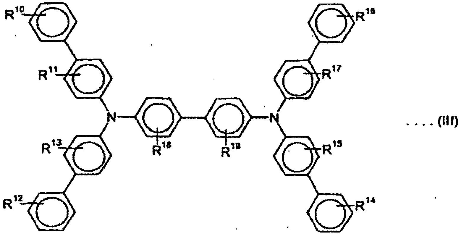 die Atome oder Gruppen, dargestellt durch R10 bis R19, gleich oder verschieden voneinander sein können.
- Organische Elektrolumineszenzvorrichtung gemäß Anspruch 1, worin das Hauptmaterial, das das lichtemittierende Material konstituiert, eine Energie eines Tripletniveaus aufweist, die größer ist als die Energie eines Tripletniveaus der organometallischen Komplexverbindung mit einem Schwermetall.
- Organische Elektrolumineszenzvorrichtung gemäß Anspruch 1 oder 2, worin ein Ligand in der organometallischen Komplexverbindung mit einem Schwermetall zumindest einen Liganden enthält, ausgewählt aus folgenden Liganden:


- Organische Elektrolumineszenzvorrichtung gemäß Anspruch 3, worin die organometallische Komplexverbindung 2 bis 4 der Liganden aufweist, die das Schwermetall koordinieren.
Applications Claiming Priority (3)
| Application Number | Priority Date | Filing Date | Title |
|---|---|---|---|
| JP2001155290 | 2001-05-24 | ||
| JP2001155290 | 2001-05-24 | ||
| PCT/JP2002/004485 WO2002094965A1 (fr) | 2001-05-24 | 2002-05-08 | Élément électroluminescent organique |
Publications (4)
| Publication Number | Publication Date |
|---|---|
| EP1391495A1 EP1391495A1 (de) | 2004-02-25 |
| EP1391495A4 EP1391495A4 (de) | 2007-04-25 |
| EP1391495B1 EP1391495B1 (de) | 2008-11-19 |
| EP1391495B2 true EP1391495B2 (de) | 2021-07-21 |
Family
ID=18999515
Family Applications (1)
| Application Number | Title | Priority Date | Filing Date |
|---|---|---|---|
| EP02724727.9A Expired - Lifetime EP1391495B2 (de) | 2001-05-24 | 2002-05-08 | Organisches elektrolumineszenzelement |
Country Status (9)
| Country | Link |
|---|---|
| US (4) | US20040131882A1 (de) |
| EP (1) | EP1391495B2 (de) |
| JP (1) | JP3981331B2 (de) |
| KR (2) | KR101000355B1 (de) |
| CN (1) | CN100377382C (de) |
| AT (1) | ATE414754T1 (de) |
| DE (2) | DE20221915U1 (de) |
| TW (1) | TWI290804B (de) |
| WO (1) | WO2002094965A1 (de) |
Families Citing this family (13)
| Publication number | Priority date | Publication date | Assignee | Title |
|---|---|---|---|---|
| JP2003109768A (ja) * | 2001-07-25 | 2003-04-11 | Toray Ind Inc | 発光素子 |
| JP3919583B2 (ja) * | 2002-04-12 | 2007-05-30 | キヤノン株式会社 | 有機発光素子 |
| US7452257B2 (en) * | 2002-12-27 | 2008-11-18 | Semiconductor Energy Laboratory Co., Ltd. | Method of manufacturing a display device |
| KR100696470B1 (ko) * | 2004-06-15 | 2007-03-19 | 삼성에스디아이 주식회사 | 유기 전계 발광 소자 |
| KR100751316B1 (ko) * | 2004-06-25 | 2007-08-22 | 삼성에스디아이 주식회사 | 유기 전계 발광 소자 |
| JPWO2007116750A1 (ja) * | 2006-03-30 | 2009-08-20 | 出光興産株式会社 | 有機エレクトロルミネッセンス素子用材料、及びこれを用いた有機エレクトロルミネッセンス素子 |
| EP2097938B1 (de) * | 2006-12-28 | 2019-07-17 | Universal Display Corporation | Phosphoreszierende oled-strukturen mit langer lebensdauer |
| US8372527B2 (en) * | 2007-07-11 | 2013-02-12 | Idemitsu Kosan Co., Ltd. | Material for organic electroluminescent element, and organic electroluminescent element |
| US8040053B2 (en) * | 2008-02-09 | 2011-10-18 | Universal Display Corporation | Organic light emitting device architecture for reducing the number of organic materials |
| KR101587307B1 (ko) * | 2008-09-04 | 2016-01-20 | 유니버셜 디스플레이 코포레이션 | 백색 인광성 유기 발광 디바이스 |
| JP2010073598A (ja) * | 2008-09-22 | 2010-04-02 | Mitsubishi Chemicals Corp | 有機薄膜パターニング用基板、有機電界発光素子、有機el表示装置および有機el照明 |
| US8288187B2 (en) | 2010-01-20 | 2012-10-16 | Universal Display Corporation | Electroluminescent devices for lighting applications |
| US9349964B2 (en) * | 2010-12-24 | 2016-05-24 | Lg Chem, Ltd. | Organic light emitting diode and manufacturing method thereof |
Citations (1)
| Publication number | Priority date | Publication date | Assignee | Title |
|---|---|---|---|---|
| US5837166A (en) † | 1993-09-29 | 1998-11-17 | Idemitsu Kosan Co., Ltd. | Organic electroluminescence device and arylenediamine derivative |
Family Cites Families (16)
| Publication number | Priority date | Publication date | Assignee | Title |
|---|---|---|---|---|
| US4720432A (en) | 1987-02-11 | 1988-01-19 | Eastman Kodak Company | Electroluminescent device with organic luminescent medium |
| DE69412567T2 (de) * | 1993-11-01 | 1999-02-04 | Hodogaya Chemical Co., Ltd., Tokio/Tokyo | Aminverbindung und sie enthaltende Elektrolumineszenzvorrichtung |
| EP0666298A3 (de) * | 1994-02-08 | 1995-11-15 | Tdk Corp | Organisches elektrolumineszentes Element und darin gebrauchte Verbindung. |
| US5707745A (en) * | 1994-12-13 | 1998-01-13 | The Trustees Of Princeton University | Multicolor organic light emitting devices |
| JP3168897B2 (ja) * | 1996-01-12 | 2001-05-21 | 出光興産株式会社 | ナフチル基を有するジアミン誘導体及び該誘導体を用いた有機エレクトロルミネッセンス素子 |
| JP3650218B2 (ja) * | 1996-05-10 | 2005-05-18 | ケミプロ化成株式会社 | 高分子量芳香族アミン化合物およびそれよりなるホール輸送性材料 |
| EP0915143A4 (de) * | 1996-06-28 | 2002-09-04 | Chisso Corp | Rotemittierendes material und unter verwendung desselben hergestellte organische elektrolumineszente vorrichtung |
| JP3764218B2 (ja) * | 1996-10-01 | 2006-04-05 | 出光興産株式会社 | 有機電界発光素子 |
| EP0891121B8 (de) * | 1996-12-28 | 2013-01-02 | Futaba Corporation | Organische elektrolumineszente elementen |
| JPH11144773A (ja) * | 1997-09-05 | 1999-05-28 | Fuji Photo Film Co Ltd | 光電変換素子および光再生型光電気化学電池 |
| JP3757583B2 (ja) * | 1997-11-17 | 2006-03-22 | 三菱化学株式会社 | 有機電界発光素子 |
| KR100662949B1 (ko) * | 1999-09-30 | 2006-12-28 | 이데미쓰 고산 가부시키가이샤 | 아민 화합물 및 이를 이용한 유기 전자발광 소자 |
| JP3938263B2 (ja) * | 1999-11-09 | 2007-06-27 | 独立行政法人科学技術振興機構 | 金属錯体の製造方法 |
| EP2270895A3 (de) * | 1999-12-01 | 2011-03-30 | The Trustees of Princeton University | Komplexe für OLED-Anwendungen |
| JP2001313178A (ja) * | 2000-04-28 | 2001-11-09 | Pioneer Electronic Corp | 有機エレクトロルミネッセンス素子 |
| US6645645B1 (en) * | 2000-05-30 | 2003-11-11 | The Trustees Of Princeton University | Phosphorescent organic light emitting devices |
-
2002
- 2002-05-08 JP JP2002592428A patent/JP3981331B2/ja not_active Expired - Lifetime
- 2002-05-08 KR KR1020087023669A patent/KR101000355B1/ko not_active Ceased
- 2002-05-08 DE DE20221915U patent/DE20221915U1/de not_active Expired - Lifetime
- 2002-05-08 KR KR10-2003-7015367A patent/KR20040012860A/ko not_active Ceased
- 2002-05-08 US US10/477,752 patent/US20040131882A1/en not_active Abandoned
- 2002-05-08 WO PCT/JP2002/004485 patent/WO2002094965A1/ja not_active Ceased
- 2002-05-08 DE DE60229934T patent/DE60229934D1/de not_active Expired - Lifetime
- 2002-05-08 CN CNB028105656A patent/CN100377382C/zh not_active Ceased
- 2002-05-08 AT AT02724727T patent/ATE414754T1/de not_active IP Right Cessation
- 2002-05-08 EP EP02724727.9A patent/EP1391495B2/de not_active Expired - Lifetime
- 2002-05-14 TW TW091110056A patent/TWI290804B/zh active
-
2006
- 2006-02-27 US US11/362,209 patent/US20060141288A1/en not_active Abandoned
-
2010
- 2010-01-07 US US12/683,793 patent/US20100109001A1/en not_active Abandoned
-
2012
- 2012-03-09 US US13/416,326 patent/US20120168740A1/en not_active Abandoned
Patent Citations (1)
| Publication number | Priority date | Publication date | Assignee | Title |
|---|---|---|---|---|
| US5837166A (en) † | 1993-09-29 | 1998-11-17 | Idemitsu Kosan Co., Ltd. | Organic electroluminescence device and arylenediamine derivative |
Non-Patent Citations (2)
| Title |
|---|
| ADACHI, KWONG AND FORREST: "Efficient electrophosphorescencence using a doped ambipolar conductive molecular organic thin film", ORGANIC ELECTRONICS, vol. 2, 2001, pages 37 - 43 † |
| JUNJI KIDO: "Organic electroluminescence materials and displays", 28 February 2001, CMC CO., LTD † |
Also Published As
| Publication number | Publication date |
|---|---|
| JPWO2002094965A1 (ja) | 2004-09-09 |
| TWI290804B (en) | 2007-12-01 |
| KR20040012860A (ko) | 2004-02-11 |
| DE20221915U1 (de) | 2009-06-04 |
| ATE414754T1 (de) | 2008-12-15 |
| CN100377382C (zh) | 2008-03-26 |
| US20060141288A1 (en) | 2006-06-29 |
| EP1391495A4 (de) | 2007-04-25 |
| US20120168740A1 (en) | 2012-07-05 |
| CN1531581A (zh) | 2004-09-22 |
| KR101000355B1 (ko) | 2010-12-13 |
| JP3981331B2 (ja) | 2007-09-26 |
| US20100109001A1 (en) | 2010-05-06 |
| US20040131882A1 (en) | 2004-07-08 |
| WO2002094965A1 (fr) | 2002-11-28 |
| EP1391495A1 (de) | 2004-02-25 |
| KR20080100278A (ko) | 2008-11-14 |
| DE60229934D1 (de) | 2009-01-02 |
| EP1391495B1 (de) | 2008-11-19 |
Similar Documents
| Publication | Publication Date | Title |
|---|---|---|
| US7429426B2 (en) | Organometallic compounds for use in electroluminescent devices | |
| US7070867B2 (en) | OLEDs having n-type doping | |
| EP2267097B1 (de) | Verbesserte Elektrolumineszenzstabilität | |
| EP1932193B1 (de) | Organische lichtemittierende Vorrichtung | |
| JP6025959B2 (ja) | 有機発光ダイオードのための2−アザトリフェニレン物質 | |
| US8105700B2 (en) | Materials and structures for enhancing the performance of organic light emitting devices | |
| EP1205527B2 (de) | Organische elektrolumineszierende vorrichtung | |
| US7029765B2 (en) | Organic light emitting devices having reduced pixel shrinkage | |
| EP1856227B1 (de) | Rot phosphoreszierende verbindungen und organische elektrolumineszenzvorrichtungen damit | |
| KR100560778B1 (ko) | 유기 전계 발광 디스플레이 장치 | |
| EP1308494B1 (de) | Organische elektrolumineszente Vorrichtung | |
| US20120168740A1 (en) | Organic electroluminescence element | |
| JP3841695B2 (ja) | 有機el素子及び有機elディスプレイ | |
| US7018723B2 (en) | Materials and structures for enhancing the performance of organic light emitting devices | |
| US6902833B2 (en) | Materials and structures for enhancing the performance or organic light emitting devices | |
| JP4880450B2 (ja) | 有機金属錯体、発光性固体、有機el素子及び有機elディスプレイ | |
| EP1784057B1 (de) | Rote phosphorezente Verbindungen und organische Elektrolumineszenz-Vorrichtungen, die diese verwenden | |
| JPWO2005076668A1 (ja) | 有機エレクトロルミネッセンス素子 | |
| JP2006269670A (ja) | 有機el素子及び有機elディスプレイ |
Legal Events
| Date | Code | Title | Description |
|---|---|---|---|
| PUAI | Public reference made under article 153(3) epc to a published international application that has entered the european phase |
Free format text: ORIGINAL CODE: 0009012 |
|
| 17P | Request for examination filed |
Effective date: 20031023 |
|
| AK | Designated contracting states |
Kind code of ref document: A1 Designated state(s): AT BE CH CY DE DK ES FI FR GB GR IE IT LI LU MC NL PT SE TR |
|
| A4 | Supplementary search report drawn up and despatched |
Effective date: 20070326 |
|
| 17Q | First examination report despatched |
Effective date: 20070625 |
|
| GRAP | Despatch of communication of intention to grant a patent |
Free format text: ORIGINAL CODE: EPIDOSNIGR1 |
|
| GRAS | Grant fee paid |
Free format text: ORIGINAL CODE: EPIDOSNIGR3 |
|
| GRAA | (expected) grant |
Free format text: ORIGINAL CODE: 0009210 |
|
| AK | Designated contracting states |
Kind code of ref document: B1 Designated state(s): AT BE CH CY DE DK ES FI FR GB GR IE IT LI LU MC NL PT SE TR |
|
| REG | Reference to a national code |
Ref country code: GB Ref legal event code: FG4D |
|
| REG | Reference to a national code |
Ref country code: CH Ref legal event code: EP |
|
| REG | Reference to a national code |
Ref country code: IE Ref legal event code: FG4D |
|
| REF | Corresponds to: |
Ref document number: 60229934 Country of ref document: DE Date of ref document: 20090102 Kind code of ref document: P |
|
| PG25 | Lapsed in a contracting state [announced via postgrant information from national office to epo] |
Ref country code: AT Free format text: LAPSE BECAUSE OF FAILURE TO SUBMIT A TRANSLATION OF THE DESCRIPTION OR TO PAY THE FEE WITHIN THE PRESCRIBED TIME-LIMIT Effective date: 20081119 Ref country code: ES Free format text: LAPSE BECAUSE OF FAILURE TO SUBMIT A TRANSLATION OF THE DESCRIPTION OR TO PAY THE FEE WITHIN THE PRESCRIBED TIME-LIMIT Effective date: 20090301 |
|
| NLV1 | Nl: lapsed or annulled due to failure to fulfill the requirements of art. 29p and 29m of the patents act | ||
| PG25 | Lapsed in a contracting state [announced via postgrant information from national office to epo] |
Ref country code: NL Free format text: LAPSE BECAUSE OF FAILURE TO SUBMIT A TRANSLATION OF THE DESCRIPTION OR TO PAY THE FEE WITHIN THE PRESCRIBED TIME-LIMIT Effective date: 20081119 |
|
| PG25 | Lapsed in a contracting state [announced via postgrant information from national office to epo] |
Ref country code: BE Free format text: LAPSE BECAUSE OF FAILURE TO SUBMIT A TRANSLATION OF THE DESCRIPTION OR TO PAY THE FEE WITHIN THE PRESCRIBED TIME-LIMIT Effective date: 20081119 Ref country code: DK Free format text: LAPSE BECAUSE OF FAILURE TO SUBMIT A TRANSLATION OF THE DESCRIPTION OR TO PAY THE FEE WITHIN THE PRESCRIBED TIME-LIMIT Effective date: 20081119 |
|
| PLBI | Opposition filed |
Free format text: ORIGINAL CODE: 0009260 |
|
| PLBI | Opposition filed |
Free format text: ORIGINAL CODE: 0009260 |
|
| PG25 | Lapsed in a contracting state [announced via postgrant information from national office to epo] |
Ref country code: SE Free format text: LAPSE BECAUSE OF FAILURE TO SUBMIT A TRANSLATION OF THE DESCRIPTION OR TO PAY THE FEE WITHIN THE PRESCRIBED TIME-LIMIT Effective date: 20090219 Ref country code: PT Free format text: LAPSE BECAUSE OF FAILURE TO SUBMIT A TRANSLATION OF THE DESCRIPTION OR TO PAY THE FEE WITHIN THE PRESCRIBED TIME-LIMIT Effective date: 20090420 |
|
| 26 | Opposition filed |
Opponent name: DRAGOTTI & ASSOCIATI SRL Effective date: 20090818 |
|
| PLAX | Notice of opposition and request to file observation + time limit sent |
Free format text: ORIGINAL CODE: EPIDOSNOBS2 |
|
| 26 | Opposition filed |
Opponent name: HODOGAYA CHEMICAL CO., LTD. Effective date: 20090818 Opponent name: MERCK PATENT GMBH Effective date: 20090819 Opponent name: DRAGOTTI & ASSOCIATI SRL Effective date: 20090818 |
|
| PG25 | Lapsed in a contracting state [announced via postgrant information from national office to epo] |
Ref country code: MC Free format text: LAPSE BECAUSE OF NON-PAYMENT OF DUE FEES Effective date: 20090531 |
|
| REG | Reference to a national code |
Ref country code: CH Ref legal event code: PL |
|
| PG25 | Lapsed in a contracting state [announced via postgrant information from national office to epo] |
Ref country code: CH Free format text: LAPSE BECAUSE OF NON-PAYMENT OF DUE FEES Effective date: 20090531 Ref country code: LI Free format text: LAPSE BECAUSE OF NON-PAYMENT OF DUE FEES Effective date: 20090531 |
|
| PLAF | Information modified related to communication of a notice of opposition and request to file observations + time limit |
Free format text: ORIGINAL CODE: EPIDOSCOBS2 |
|
| PLBB | Reply of patent proprietor to notice(s) of opposition received |
Free format text: ORIGINAL CODE: EPIDOSNOBS3 |
|
| PG25 | Lapsed in a contracting state [announced via postgrant information from national office to epo] |
Ref country code: IE Free format text: LAPSE BECAUSE OF NON-PAYMENT OF DUE FEES Effective date: 20090508 |
|
| PLBP | Opposition withdrawn |
Free format text: ORIGINAL CODE: 0009264 |
|
| PG25 | Lapsed in a contracting state [announced via postgrant information from national office to epo] |
Ref country code: GR Free format text: LAPSE BECAUSE OF FAILURE TO SUBMIT A TRANSLATION OF THE DESCRIPTION OR TO PAY THE FEE WITHIN THE PRESCRIBED TIME-LIMIT Effective date: 20090220 |
|
| PG25 | Lapsed in a contracting state [announced via postgrant information from national office to epo] |
Ref country code: IT Free format text: LAPSE BECAUSE OF FAILURE TO SUBMIT A TRANSLATION OF THE DESCRIPTION OR TO PAY THE FEE WITHIN THE PRESCRIBED TIME-LIMIT Effective date: 20081119 |
|
| PG25 | Lapsed in a contracting state [announced via postgrant information from national office to epo] |
Ref country code: LU Free format text: LAPSE BECAUSE OF NON-PAYMENT OF DUE FEES Effective date: 20090508 |
|
| PG25 | Lapsed in a contracting state [announced via postgrant information from national office to epo] |
Ref country code: TR Free format text: LAPSE BECAUSE OF FAILURE TO SUBMIT A TRANSLATION OF THE DESCRIPTION OR TO PAY THE FEE WITHIN THE PRESCRIBED TIME-LIMIT Effective date: 20081119 |
|
| PG25 | Lapsed in a contracting state [announced via postgrant information from national office to epo] |
Ref country code: CY Free format text: LAPSE BECAUSE OF FAILURE TO SUBMIT A TRANSLATION OF THE DESCRIPTION OR TO PAY THE FEE WITHIN THE PRESCRIBED TIME-LIMIT Effective date: 20081119 |
|
| PGFP | Annual fee paid to national office [announced via postgrant information from national office to epo] |
Ref country code: GB Payment date: 20140507 Year of fee payment: 13 |
|
| PGFP | Annual fee paid to national office [announced via postgrant information from national office to epo] |
Ref country code: FR Payment date: 20140509 Year of fee payment: 13 Ref country code: FI Payment date: 20140512 Year of fee payment: 13 |
|
| GBPC | Gb: european patent ceased through non-payment of renewal fee |
Effective date: 20150508 |
|
| PG25 | Lapsed in a contracting state [announced via postgrant information from national office to epo] |
Ref country code: FI Free format text: LAPSE BECAUSE OF NON-PAYMENT OF DUE FEES Effective date: 20150508 |
|
| REG | Reference to a national code |
Ref country code: FR Ref legal event code: ST Effective date: 20160129 |
|
| PG25 | Lapsed in a contracting state [announced via postgrant information from national office to epo] |
Ref country code: GB Free format text: LAPSE BECAUSE OF NON-PAYMENT OF DUE FEES Effective date: 20150508 |
|
| PG25 | Lapsed in a contracting state [announced via postgrant information from national office to epo] |
Ref country code: FR Free format text: LAPSE BECAUSE OF NON-PAYMENT OF DUE FEES Effective date: 20150601 |
|
| APBM | Appeal reference recorded |
Free format text: ORIGINAL CODE: EPIDOSNREFNO |
|
| APBP | Date of receipt of notice of appeal recorded |
Free format text: ORIGINAL CODE: EPIDOSNNOA2O |
|
| PLAB | Opposition data, opponent's data or that of the opponent's representative modified |
Free format text: ORIGINAL CODE: 0009299OPPO |
|
| APAH | Appeal reference modified |
Free format text: ORIGINAL CODE: EPIDOSCREFNO |
|
| R26 | Opposition filed (corrected) |
Opponent name: HODOGAYA CHEMICAL CO., LTD. Effective date: 20090818 |
|
| APBQ | Date of receipt of statement of grounds of appeal recorded |
Free format text: ORIGINAL CODE: EPIDOSNNOA3O |
|
| APBU | Appeal procedure closed |
Free format text: ORIGINAL CODE: EPIDOSNNOA9O |
|
| PLAY | Examination report in opposition despatched + time limit |
Free format text: ORIGINAL CODE: EPIDOSNORE2 |
|
| PLBC | Reply to examination report in opposition received |
Free format text: ORIGINAL CODE: EPIDOSNORE3 |
|
| PLAY | Examination report in opposition despatched + time limit |
Free format text: ORIGINAL CODE: EPIDOSNORE2 |
|
| PLBC | Reply to examination report in opposition received |
Free format text: ORIGINAL CODE: EPIDOSNORE3 |
|
| RIC2 | Information provided on ipc code assigned after grant |
Ipc: H05B 33/22 20060101ALI20200916BHEP Ipc: H01L 51/00 20060101ALI20200916BHEP Ipc: C09K 11/06 20060101AFI20200916BHEP Ipc: H01L 51/50 20060101ALI20200916BHEP Ipc: H05B 33/14 20060101ALI20200916BHEP |
|
| PUAH | Patent maintained in amended form |
Free format text: ORIGINAL CODE: 0009272 |
|
| STAA | Information on the status of an ep patent application or granted ep patent |
Free format text: STATUS: PATENT MAINTAINED AS AMENDED |
|
| 27A | Patent maintained in amended form |
Effective date: 20210721 |
|
| AK | Designated contracting states |
Kind code of ref document: B2 Designated state(s): AT BE CH CY DE DK ES FI FR GB GR IE IT LI LU MC NL PT SE TR |
|
| REG | Reference to a national code |
Ref country code: DE Ref legal event code: R102 Ref document number: 60229934 Country of ref document: DE |
|
| PGFP | Annual fee paid to national office [announced via postgrant information from national office to epo] |
Ref country code: DE Payment date: 20210413 Year of fee payment: 20 |
|
| REG | Reference to a national code |
Ref country code: DE Ref legal event code: R071 Ref document number: 60229934 Country of ref document: DE |