EP1396757A2 - System zur Fokusmessung eines Retikels und Verfahren unter Verwendung von verschiedenen interferometrischen Strahlen - Google Patents
System zur Fokusmessung eines Retikels und Verfahren unter Verwendung von verschiedenen interferometrischen Strahlen Download PDFInfo
- Publication number
- EP1396757A2 EP1396757A2 EP03019984A EP03019984A EP1396757A2 EP 1396757 A2 EP1396757 A2 EP 1396757A2 EP 03019984 A EP03019984 A EP 03019984A EP 03019984 A EP03019984 A EP 03019984A EP 1396757 A2 EP1396757 A2 EP 1396757A2
- Authority
- EP
- European Patent Office
- Prior art keywords
- reticle
- plane
- beams
- reticle stage
- reflecting
- Prior art date
- Legal status (The legal status is an assumption and is not a legal conclusion. Google has not performed a legal analysis and makes no representation as to the accuracy of the status listed.)
- Withdrawn
Links
Images



Classifications
-
- G—PHYSICS
- G03—PHOTOGRAPHY; CINEMATOGRAPHY; ANALOGOUS TECHNIQUES USING WAVES OTHER THAN OPTICAL WAVES; ELECTROGRAPHY; HOLOGRAPHY
- G03F—PHOTOMECHANICAL PRODUCTION OF TEXTURED OR PATTERNED SURFACES, e.g. FOR PRINTING, FOR PROCESSING OF SEMICONDUCTOR DEVICES; MATERIALS THEREFOR; ORIGINALS THEREFOR; APPARATUS SPECIALLY ADAPTED THEREFOR
- G03F9/00—Registration or positioning of originals, masks, frames, photographic sheets or textured or patterned surfaces, e.g. automatically
- G03F9/70—Registration or positioning of originals, masks, frames, photographic sheets or textured or patterned surfaces, e.g. automatically for microlithography
- G03F9/7003—Alignment type or strategy, e.g. leveling, global alignment
- G03F9/7023—Aligning or positioning in direction perpendicular to substrate surface
- G03F9/7026—Focusing
-
- H—ELECTRICITY
- H10—SEMICONDUCTOR DEVICES; ELECTRIC SOLID-STATE DEVICES NOT OTHERWISE PROVIDED FOR
- H10P—GENERIC PROCESSES OR APPARATUS FOR THE MANUFACTURE OR TREATMENT OF DEVICES COVERED BY CLASS H10
- H10P76/00—Manufacture or treatment of masks on semiconductor bodies, e.g. by lithography or photolithography
-
- G—PHYSICS
- G03—PHOTOGRAPHY; CINEMATOGRAPHY; ANALOGOUS TECHNIQUES USING WAVES OTHER THAN OPTICAL WAVES; ELECTROGRAPHY; HOLOGRAPHY
- G03F—PHOTOMECHANICAL PRODUCTION OF TEXTURED OR PATTERNED SURFACES, e.g. FOR PRINTING, FOR PROCESSING OF SEMICONDUCTOR DEVICES; MATERIALS THEREFOR; ORIGINALS THEREFOR; APPARATUS SPECIALLY ADAPTED THEREFOR
- G03F7/00—Photomechanical, e.g. photolithographic, production of textured or patterned surfaces, e.g. printing surfaces; Materials therefor, e.g. comprising photoresists; Apparatus specially adapted therefor
- G03F7/70—Microphotolithographic exposure; Apparatus therefor
- G03F7/70691—Handling of masks or workpieces
- G03F7/70716—Stages
-
- G—PHYSICS
- G03—PHOTOGRAPHY; CINEMATOGRAPHY; ANALOGOUS TECHNIQUES USING WAVES OTHER THAN OPTICAL WAVES; ELECTROGRAPHY; HOLOGRAPHY
- G03F—PHOTOMECHANICAL PRODUCTION OF TEXTURED OR PATTERNED SURFACES, e.g. FOR PRINTING, FOR PROCESSING OF SEMICONDUCTOR DEVICES; MATERIALS THEREFOR; ORIGINALS THEREFOR; APPARATUS SPECIALLY ADAPTED THEREFOR
- G03F7/00—Photomechanical, e.g. photolithographic, production of textured or patterned surfaces, e.g. printing surfaces; Materials therefor, e.g. comprising photoresists; Apparatus specially adapted therefor
- G03F7/70—Microphotolithographic exposure; Apparatus therefor
- G03F7/70691—Handling of masks or workpieces
- G03F7/70716—Stages
- G03F7/70725—Stages control
Definitions
- the present invention relates to controlling a reticle stage during exposure.
- a mounting side and a patterned side of a reticle are one and the same, establishing a reticle focal plane at a plane of a reticle stage platen.
- stage position in six degrees-of-freedom (DOF) resulted in knowledge of the reticle patterned surface position in six DOF.
- the six DOF are X, Y, Z, Rx, Ry, and Rz, as shown in FIG. 1.
- mounting (or clamping) of an extreme ultra violet (EUV) reticle will almost certainly be to a back surface of the reticle (e.g., opposite from the patterned surface).
- EUV extreme ultra violet
- Backside clamping results in a reticle focal plane position relative to the reticle stage that is a function of reticle flatness, reticle thickness, and reticle thickness variation.
- knowledge of the reticle stage position does not resolve where the pattern of the reticle is located in all six DOF.
- the out-of-plane DOF (Z, Rx, and Ry) cannot be easily determined due to the thickness variation of the reticle.
- the position of the patterned side (opposite to the clamped side) of the reticle needs to be known accurately in all six DOF.
- a measuring system and method that can easily calibrate or correlate a reticle.
- focal plane for a backside clamped reticle
- a measuring system and method is also needed that maps a reticle surface to surfaces on a reticle stage, which allows feedback for stage position to be based on surfaces on the stage instead of surfaces on the reticle surface.
- Embodiments of the present invention provide a method including the steps of measuring location data of a pattern side of a reticle based on a first set of interferometer measuring beams; measuring map data of a reticle stage during scanning of the reticle stage based on a second set of interferometer measuring beams, and controlling the reticle stage during exposure of a wafer with a pattern on the pattern side of the reticle based on the location data and the map data.
- Still further embodiments of the present invention provide a system including a moveable reticle stage holding a reticle, the reticle having a patterned side, a dual interferometer device that projects and detects a first set of interferometer beams from the patterned side of the reticle and a second set of interferometer beams from the reticle stage, and a storage device that stores location data of the reticle measured by the first set of interferometer beams and map data of the reticle stage measured by the second set of interferometer beams.
- FIG. 1 shows an example orientation of a reticle according to embodiments of the present invention.
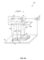
- FIG. 2A shows a portion of a lithographic system or tool using a dual interferometer according to embodiments of the present invention.
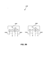
- FIG. 2B shows a portion of a lithographic system using two interferometers according to embodiments of the present invention.
- FIGS. 3A and 3B show various configurations of a reticle and a stage being measured according to various embodiments of the present invention.
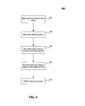
- FIG. 4 shows a flowchart of an overall measuring and controlling method for a lithography tool according to embodiments of the present invention.
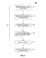
- FIG. 5 shows a flowchart of a measuring and controlling method for a reticle according to embodiments of the present invention.
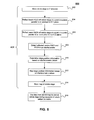
- FIG. 6 shows a flowchart of a measuring and controlling method for a reticle stage according to embodiments of the present invention.
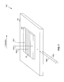
- FIG. 7 shows a portion of a lithographic system for measuring reticle and stage positions according to embodiments of the present invention.
- FIG. 8 shows a portion of a lithographic system for measuring reticle and stage positions according to embodiments of the present invention.
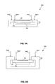
- FIG. 9A shows a portion of a lithographic system having a side held reticle according to embodiments of the present invention.
- FIG. 9B shows a portion of a lithographic system having a front held reticle according to embodiments of the present invention.
- a first set of interferometric measuring beams is used to determine a location of a patterned surface of a reticle and a reticle focus plane for a reticle that is clamped (e.g., back, side, or front clamped) to a reticle stage.
- a second set of interferometric measuring beams is used to determine a map of locations of the reticle stage during scanning in a Y direction.
- the two sets of interferometric measuring beams are correlated to relate the reticle focal plane to the map of the reticle stage.
- the information is used to control the reticle stage during exposure of a pattern on the patterned surface of the reticle onto a wafer.
- FIG. 1 shows six degrees of freedom (DOF) for a reticle 100 oriented in or parallel to an X-Y plane according to embodiments of the present invention.
- the six DOF are X (along the X axis), Y (along the Y axis), Z (along the Z axis), Rx (rotation around the X axis), Ry (rotation around the Y axis), and Rz (rotation around the Z axis).
- the more easily determinable DOF are the X, Y, and Rz based on a reticle stage's movements.
- the DOF that are the focus of the discussion below are Z and Ry. It is to be appreciated that any DOF can be determined by the appatarus and methods below if the orientation of the reticle 100 is changed.
- FIG. 2A shows a portion 200 of a lithography tool according to embodiments of the present invention.
- Portion 200 includes a reticle stage 202 with a backside clamped reticle 204 that has a pattern 206.
- an interferometer system 208 includes two interferometers 208A and 208B. Each interferometer 208A and 208B projects illuminating (I) light from illumination devices 210 towards portion 200.
- illumination devices 210 can be light sources, lasers, or the like with or without focusing or expanding optical devices.
- a first set of interferometric measuring beams RSZ1 and RSZ2 from first interferometer 208A are reflected from first 212 and second 214 positions, respectively, on reticle 204.
- First position 212 is adjacent a first side of pattern 206 and second position 214 is adjacent a second side of pattern 206.
- the reflected beams are received by detectors (D) 216.
- Signals corresponding to the detected beams are stored in a storage device 218 either before or after being processed by controller 220.
- a second set of interferometric measuring beams RSZ3 and RSZ4 from second interferometer 208B are reflected from first 222 and second 224 points, respectively, on reticle stage 202 and detected by detectors 216. Signals correlating to the detected beams are then stored in storage 218.
- all four measuring points, 212, 214, 222, and 224 substantially lie along a line having a same Y value. In other embodiments this may be required.
- FIG. 2B shows an interferometer 208' including a first interferometer 208A' and a second interferometer 208B' according to embodiments of the present invention.
- FIGS. 3A and 3B show a first and second posisble position of reticle 204 according to embodiments of the present invention.
- interferometric techniques are performed by the interferometer system 208 or 208' and values are determined by controller 220 (FIG. 2A).
- signals represent an interferometric measurement based on either intensity, phase, distance, or the like of two related beams (i.e., RSZ1 and RSZ2 or RSZ3 and RSZ4) being compared.
- a resulting signal from the comparison corresponds to paramaters (e.g., position, orientation, tilt, etc.) of either reticle stage 202 or reticle 204.
- the calculation of Z and Ry is as follows for a reticle 204 that lies on or parallel to the Y axis.
- Z1 is approximately equal to Z2 because reticle 204 lies in or parallel to the Y-axis.
- Ry it is substantially zero. This is because, if Z1 ⁇ Z2, then Z2-Z1 ⁇ 0.
- the calculation of Z and RY is as follows for a reticle that is rotated Ry around the Y axis.
- Z it is equal to (Z1+Z2)/2, or the average of the two values.
- Ry it is, equal to (Z2-Z1)/L, as is shown in the equation above.
- the four interferometer beams RSZ1-RSZ4 are used to determine two DOF (Z and Ry) of the patterned surface 206 of reticle 204.
- Z is a direction about normal to the patterned surface 206 and parallel to the lithographic tool's optical axis.
- Ry is a rotation about a scan axis of the reticle stage 202.
- two interferometer beams (RSZ1. and RSZ2) reflect off of pattern surface 206 of reticle 204 on either side of the pattern 206. These beams cannot be used during lithographic printing because the reticle stage 202 has to travel (in the scan Y direction shown as an arrow in FIGs.
- the other two interferometer beams are positioned to reflect off of surfaces on the reticle stage 202.
- a first reflective surface e.g., with point 222
- a second reflective surface e.g., with point 224
- the second reflective surface of reticle stage 202 can be oriented in or parallel to a Y-Z plane.
- the second surface yields Ry stage position information.
- various other orientations exist where calculations would yield Z and Ry values.
- the lithographic tool would typically look at the difference between two interferometers (e.g., dual interferometer 210 or interferometers 210A' and 210B') with separation in either the X or Z directions, thus giving Ry information.
- FIGS. 4-6 show flowcharts of methods 400, 500, and 600 according to embodiments of the present invention. A summary of those methods follows. After loading reticle 204 (and occasionally during calibration or between calibrations once or periodically) onto reticle stage 202 the data from RSZ1 and RSZ2 can be used to locate the patterned surface 206 at a reticle focal plane established by projection optics (not shown) of the lithography tool or any other desired plane determined by machine setup. Then, while reticle stage 202 is scanned in the Y direction so that reticle 204 remains in the chosen plane, the values of RSZ3 and RSZ4 are recorded and stored as a map.
- the data from the map will be used to control the reticle stage 202, and thereby the reticle 204, in Z and Ry so that pattern 206 is always in the chosen plane.
- the stage control is not compromised because the control feedback is coming from beams RSZ3 and RSZ4.
- beams RSZ1 and RSZ2 can be constantly monitored during lithography to verify the map and to possibly do continuous updating of the map used for stage Z and Ry control. It is to be appreciated that there are other ways of determining stage position during scanning while maintaining pattern 206 of reticle 204 in a chosen plane, which are all contemplated by the invention.
- FIG. 4 depicts a flowchart of method 400 according to embodiments of the present invention (steps 402-410).
- a reticle e.g., reticle 20
- a reticle stage e.g., stage 202
- a reticle focal plane is determined based on a first set of interferometric measuring beams (e.g., RSZ1 and RSZ2).
- a map of reticle stage locations is determined during scanning of the reticle stage based on a second set of interferometric measuring beams (e.g., RSZ3 and RSZ4).
- the measured reticle focal plane is correlated to the map of the reticle stage.
- the reticle stage is controlled based on the correlation during exposure of a pattern on the reticle onto a wafer. The exposure is accomplished through processes known in the art.
- FIG. 5 depicts a flowchart of method 500 that can occur during step 406 according to embodiments of the present invention.
- a first beam e.g., RSZ1
- a second beam e.g., RSZ2
- a location e.g., point 214 adjacent a second side of the reticle pattern.
- the two reflected beams are detected in an interferometer (e.g., interferometer 208 or 208').
- an interferometric operation is performed (e.g., in controller 220) on the received signals to determine a location of the reticle pattern, and thus the reticle focus plane.
- location information is stored (e.g., in storage 218).
- the location information is used (e.g., by stage controller 228) to control a reticle stage (e.g., stage 202) during an exposure process.
- FIG. 6 depicts a flowchart of a method 600 that can occur during step 408 according to embodiments of the present invention.
- a reticle stage e.g., stage 202
- a first measuring beam e.g., RSZ3
- a second measuring beam e.g., RSZ4
- a point e.g., point 224 on the reticle stage that is parallel to or oriented in the X-Y or Y-Z plane.
- the first and second measuring beams are detected by an interferometer (e.g., interferometers 208 or 208').
- stage position information is determined (e.g., by processor 220) based on interferometric values generated by the interferometer.
- a map is generated (e.g., by controller 220) of the stage position during the scan based on the interferometric values.
- the map is stored (e.g., in storage 218).
- data from the stored map is used (e.g., by stage controller 228) to control the reticle stage during an exposure process.
- FIG. 7 shows a portion 700 of a lithography tool used to measure stage 202 and reticle 204 positions according to embodiments of the present invention.
- beams RSZ1-RSZ3 and RSX1-RSX2 are produced by and detected by an interferometer similar to 208 or 208' discussed above, or any other interferometer.
- RSZ1 and RSZ2 are used to determined characteristics about reticle 204 and RSZ3 is used to determine Z of stage 202.
- FIG. 8 shows a portion 800 of a lithography tool used to measure stage 202 and reticle 204 positions according to embodiments of the present invention.
- beams RSZ1-RSZ5, RSY1-RSY3, and RSX1 are produced by and detected by an interferometer similar to 208 or 208' discussed above, or any other interferometer.
- This embodiment shows beams that can enable determination of all six DOF for stage 202 and/or reticle 204.
- Beams RSZ1 and RSZ2 allow for Z and Ry of reticle 204 to be determined.
- Beams RSZ1 and RSZ5 allows for RX of reticle 204 to be determined.
- Beams RSZ3 and RSZ4 allow for Z and Ry of stage 202 to be determined.
- Beam RSX1 allows for X of stage 202 to be determined.
- Beam RSY1, RSY2, and/or RSY3 allow for Y of stage 202 to be determined.
- Beams RSY2 and RSY3 allow for Rz of stage 202 to be determined.
- Beams RSY1 and RSY3 allow for Rx of stage 202 to be determined.
- FIG. 9A shows a portion 900 of a lithography tool according to embodiments of the present invention.
- Portion 900 includes reticle 204 that is clamped at its sides to stage 902.
- reticle 204 can be coupled to a support device (e.g., a stiffener) 904 to counteract any warping force on reticle 202.
- Beams RSZ1-RSZ4 can be used as described above to determine Z and Ry of stage 902 and/or reticle 204.
- FIG. 9B shows a portion 920 of a lithography tool according to embodiments of the present invention.
- Portion 920 includes reticle 204 that is front clamped to stage 922.
- reticle 204 can be coupled to support device 904 to counteract any warping force on reticle 202.
- Beams RSZ1-RSZ4 can be used as described above to determined Z and Ry of stage 922 and/or reticle 204.
Landscapes
- Physics & Mathematics (AREA)
- General Physics & Mathematics (AREA)
- Exposure And Positioning Against Photoresist Photosensitive Materials (AREA)
- Exposure Of Semiconductors, Excluding Electron Or Ion Beam Exposure (AREA)
- Preparing Plates And Mask In Photomechanical Process (AREA)
Applications Claiming Priority (4)
| Application Number | Priority Date | Filing Date | Title |
|---|---|---|---|
| US417257 | 1982-09-13 | ||
| US235499 | 2002-09-06 | ||
| US10/235,499 US6934005B2 (en) | 2002-09-06 | 2002-09-06 | Reticle focus measurement method using multiple interferometric beams |
| US10/417,257 US6850330B2 (en) | 2002-09-06 | 2003-04-17 | Reticle focus measurement system using multiple interferometric beams |
Publications (2)
| Publication Number | Publication Date |
|---|---|
| EP1396757A2 true EP1396757A2 (de) | 2004-03-10 |
| EP1396757A3 EP1396757A3 (de) | 2008-12-17 |
Family
ID=31720202
Family Applications (1)
| Application Number | Title | Priority Date | Filing Date |
|---|---|---|---|
| EP03019984A Withdrawn EP1396757A3 (de) | 2002-09-06 | 2003-09-03 | System zur Fokusmessung eines Retikels und Verfahren unter Verwendung von verschiedenen interferometrischen Strahlen |
Country Status (6)
| Country | Link |
|---|---|
| US (1) | US7016051B2 (de) |
| EP (1) | EP1396757A3 (de) |
| JP (1) | JP3831720B2 (de) |
| KR (1) | KR100670072B1 (de) |
| CN (1) | CN1510525A (de) |
| SG (1) | SG107671A1 (de) |
Cited By (3)
| Publication number | Priority date | Publication date | Assignee | Title |
|---|---|---|---|---|
| WO2006068288A1 (ja) | 2004-12-22 | 2006-06-29 | Nikon Corporation | マスク表面の高さ方向位置測定方法、露光装置及び露光方法 |
| EP1803029A4 (de) * | 2004-10-18 | 2010-07-21 | Nikon Corp | Verfahren und vorrichtung mit einem retikelstufensicherheitsmerkmal |
| US7853067B2 (en) | 2006-10-27 | 2010-12-14 | Asml Holding N.V. | Systems and methods for lithographic reticle inspection |
Families Citing this family (3)
| Publication number | Priority date | Publication date | Assignee | Title |
|---|---|---|---|---|
| US7894038B2 (en) * | 2007-03-14 | 2011-02-22 | Asml Netherlands B.V. | Device manufacturing method, lithographic apparatus, and a computer program |
| CN101493655B (zh) * | 2008-01-21 | 2011-07-20 | 联华电子股份有限公司 | 曝光方法 |
| TWI512405B (zh) * | 2009-08-07 | 2015-12-11 | 尼康股份有限公司 | A moving body device, an exposure apparatus, and an element manufacturing method |
Family Cites Families (11)
| Publication number | Priority date | Publication date | Assignee | Title |
|---|---|---|---|---|
| KR100254024B1 (ko) * | 1990-07-23 | 2000-06-01 | 가나이 쓰도무 | 반도체 장치의 제조 방법 |
| JPH09180989A (ja) * | 1995-12-26 | 1997-07-11 | Toshiba Corp | 露光装置および露光方法 |
| JPH10335234A (ja) * | 1997-05-29 | 1998-12-18 | Nikon Corp | 投影露光装置 |
| IL135139A0 (en) * | 1997-09-19 | 2001-05-20 | Nikon Corp | Stage apparatus, scanning type exposure apparatus, and device produced with the same |
| EP1039510A4 (de) * | 1997-11-14 | 2003-11-12 | Nikon Corp | Belichtungsapparat und herstellungsverfahren, und belichtungsverfahren |
| AU2549899A (en) * | 1998-03-02 | 1999-09-20 | Nikon Corporation | Method and apparatus for exposure, method of manufacture of exposure tool, device, and method of manufacture of device |
| JPH11307436A (ja) * | 1998-04-27 | 1999-11-05 | Fujitsu Ltd | 投影露光装置及びレチクル及びレチクルの位置決め方法 |
| US6768124B2 (en) * | 1999-10-19 | 2004-07-27 | Nikon Corporation | Reticle-focus detector, and charged-particle-beam microlithography apparatus and methods comprising same |
| JP3728180B2 (ja) * | 2000-06-01 | 2005-12-21 | キヤノン株式会社 | 干渉計搭載ステージ |
| AU2003252349A1 (en) * | 2002-07-31 | 2004-02-16 | Nikon Corporation | Position measuring method, position control method, exposure method and exposure apparatus, and device manufacturing method |
| US6934005B2 (en) * | 2002-09-06 | 2005-08-23 | Asml Holding N.V. | Reticle focus measurement method using multiple interferometric beams |
-
2003
- 2003-09-03 EP EP03019984A patent/EP1396757A3/de not_active Withdrawn
- 2003-09-03 SG SG200305649A patent/SG107671A1/en unknown
- 2003-09-05 CN CNA03155430XA patent/CN1510525A/zh active Pending
- 2003-09-06 KR KR1020030062321A patent/KR100670072B1/ko not_active Expired - Fee Related
- 2003-09-08 JP JP2003315916A patent/JP3831720B2/ja not_active Expired - Fee Related
-
2004
- 2004-10-15 US US10/965,026 patent/US7016051B2/en not_active Expired - Fee Related
Cited By (4)
| Publication number | Priority date | Publication date | Assignee | Title |
|---|---|---|---|---|
| EP1803029A4 (de) * | 2004-10-18 | 2010-07-21 | Nikon Corp | Verfahren und vorrichtung mit einem retikelstufensicherheitsmerkmal |
| WO2006068288A1 (ja) | 2004-12-22 | 2006-06-29 | Nikon Corporation | マスク表面の高さ方向位置測定方法、露光装置及び露光方法 |
| EP1830395A4 (de) * | 2004-12-22 | 2010-06-30 | Nikon Corp | Verfahren zur messung der position einer maskenoberfläche in der höhenrichtung, belichtungsvorrichtung und belichtungsverfahren |
| US7853067B2 (en) | 2006-10-27 | 2010-12-14 | Asml Holding N.V. | Systems and methods for lithographic reticle inspection |
Also Published As
| Publication number | Publication date |
|---|---|
| KR100670072B1 (ko) | 2007-01-18 |
| US7016051B2 (en) | 2006-03-21 |
| SG107671A1 (en) | 2004-12-29 |
| CN1510525A (zh) | 2004-07-07 |
| KR20040022401A (ko) | 2004-03-12 |
| US20050062980A1 (en) | 2005-03-24 |
| EP1396757A3 (de) | 2008-12-17 |
| JP2004104130A (ja) | 2004-04-02 |
| JP3831720B2 (ja) | 2006-10-11 |
Similar Documents
| Publication | Publication Date | Title |
|---|---|---|
| US5502311A (en) | Method of and apparatus for detecting plane position | |
| JP4332486B2 (ja) | 時間を節約する高さ測定を用いた、基板にマスク・パターンを繰り返し投影する方法および装置 | |
| US6287734B2 (en) | Exposure method | |
| US6376329B1 (en) | Semiconductor wafer alignment using backside illumination | |
| US6618119B2 (en) | Projection exposure method and apparatus | |
| JPH09275072A (ja) | 移動鏡の真直度誤差補正方法及びステージ装置 | |
| US20090262323A1 (en) | Measurement apparatus, exposure apparatus, and device manufacturing method | |
| JPH1145846A (ja) | 走査型露光方法及び装置 | |
| US6226087B1 (en) | Method for measuring the positions of structures on a mask surface | |
| US6934005B2 (en) | Reticle focus measurement method using multiple interferometric beams | |
| US6674512B2 (en) | Interferometer system for a semiconductor exposure system | |
| US7016051B2 (en) | Reticle focus measurement system using multiple interferometric beams | |
| US20050041235A1 (en) | Exposure apparatus, method of controlling same, and method of manufacturing devices | |
| JPH11186129A (ja) | 走査型露光方法及び装置 | |
| US7382469B2 (en) | Exposure apparatus for manufacturing semiconductor device, method of exposing a layer of photoresist, and method of detecting vibrations and measuring relative position of substrate during an exposure process | |
| JPH09246356A (ja) | 表面位置設定方法 | |
| JPH11214289A (ja) | 位置計測方法、及び該方法を用いる露光方法 | |
| JPH1050600A (ja) | 投影露光方法及び投影露光装置 | |
| JPH06104158A (ja) | 位置検出装置 | |
| JPH09199573A (ja) | 位置決めステージ装置およびこれを用いた露光装置 | |
| KR100629390B1 (ko) | 광학계 위치제어수단을 갖는 반도체 제조용 노광장치 및이를 이용한 노광방법 | |
| JP7022611B2 (ja) | 露光装置の制御方法、露光装置、及び物品製造方法 | |
| JP2023077924A (ja) | 露光装置、露光方法、および物品製造方法 | |
| JP2000031016A (ja) | 露光方法及び装置 | |
| JPH10275768A (ja) | 投影露光装置及び相対位置計測方法 |
Legal Events
| Date | Code | Title | Description |
|---|---|---|---|
| PUAI | Public reference made under article 153(3) epc to a published international application that has entered the european phase |
Free format text: ORIGINAL CODE: 0009012 |
|
| AK | Designated contracting states |
Kind code of ref document: A2 Designated state(s): AT BE BG CH CY CZ DE DK EE ES FI FR GB GR HU IE IT LI LU MC NL PT RO SE SI SK TR |
|
| AX | Request for extension of the european patent |
Extension state: AL LT LV MK |
|
| RAP1 | Party data changed (applicant data changed or rights of an application transferred) |
Owner name: ASML HOLDING N.V. |
|
| PUAL | Search report despatched |
Free format text: ORIGINAL CODE: 0009013 |
|
| AK | Designated contracting states |
Kind code of ref document: A3 Designated state(s): AT BE BG CH CY CZ DE DK EE ES FI FR GB GR HU IE IT LI LU MC NL PT RO SE SI SK TR |
|
| AX | Request for extension of the european patent |
Extension state: AL LT LV MK |
|
| AKX | Designation fees paid | ||
| REG | Reference to a national code |
Ref country code: DE Ref legal event code: 8566 |
|
| STAA | Information on the status of an ep patent application or granted ep patent |
Free format text: STATUS: THE APPLICATION IS DEEMED TO BE WITHDRAWN |
|
| 18D | Application deemed to be withdrawn |
Effective date: 20090618 |