EP1396884A2 - Couche isolante intermédiaire pour un circuit multicouche interconnecté et procédé de fabrication - Google Patents
Couche isolante intermédiaire pour un circuit multicouche interconnecté et procédé de fabrication Download PDFInfo
- Publication number
- EP1396884A2 EP1396884A2 EP03020250A EP03020250A EP1396884A2 EP 1396884 A2 EP1396884 A2 EP 1396884A2 EP 03020250 A EP03020250 A EP 03020250A EP 03020250 A EP03020250 A EP 03020250A EP 1396884 A2 EP1396884 A2 EP 1396884A2
- Authority
- EP
- European Patent Office
- Prior art keywords
- insulation film
- gas
- silicon
- containing hydrocarbon
- less
- Prior art date
- Legal status (The legal status is an assumption and is not a legal conclusion. Google has not performed a legal analysis and makes no representation as to the accuracy of the status listed.)
- Withdrawn
Links
- 0 *[Si+]1O[S+](*)OS(*)O1 Chemical compound *[Si+]1O[S+](*)OS(*)O1 0.000 description 1
Images
Classifications
-
- H—ELECTRICITY
- H10—SEMICONDUCTOR DEVICES; ELECTRIC SOLID-STATE DEVICES NOT OTHERWISE PROVIDED FOR
- H10P—GENERIC PROCESSES OR APPARATUS FOR THE MANUFACTURE OR TREATMENT OF DEVICES COVERED BY CLASS H10
- H10P14/00—Formation of materials, e.g. in the shape of layers or pillars
- H10P14/60—Formation of materials, e.g. in the shape of layers or pillars of insulating materials
- H10P14/69—Inorganic materials
- H10P14/692—Inorganic materials composed of oxides, glassy oxides or oxide-based glasses
- H10P14/6921—Inorganic materials composed of oxides, glassy oxides or oxide-based glasses containing silicon
- H10P14/6922—Inorganic materials composed of oxides, glassy oxides or oxide-based glasses containing silicon the material containing Si, O and at least one of H, N, C, F or other non-metal elements, e.g. SiOC, SiOC:H or SiONC
-
- C—CHEMISTRY; METALLURGY
- C23—COATING METALLIC MATERIAL; COATING MATERIAL WITH METALLIC MATERIAL; CHEMICAL SURFACE TREATMENT; DIFFUSION TREATMENT OF METALLIC MATERIAL; COATING BY VACUUM EVAPORATION, BY SPUTTERING, BY ION IMPLANTATION OR BY CHEMICAL VAPOUR DEPOSITION, IN GENERAL; INHIBITING CORROSION OF METALLIC MATERIAL OR INCRUSTATION IN GENERAL
- C23C—COATING METALLIC MATERIAL; COATING MATERIAL WITH METALLIC MATERIAL; SURFACE TREATMENT OF METALLIC MATERIAL BY DIFFUSION INTO THE SURFACE, BY CHEMICAL CONVERSION OR SUBSTITUTION; COATING BY VACUUM EVAPORATION, BY SPUTTERING, BY ION IMPLANTATION OR BY CHEMICAL VAPOUR DEPOSITION, IN GENERAL
- C23C16/00—Chemical coating by decomposition of gaseous compounds, without leaving reaction products of surface material in the coating, i.e. chemical vapour deposition [CVD] processes
- C23C16/22—Chemical coating by decomposition of gaseous compounds, without leaving reaction products of surface material in the coating, i.e. chemical vapour deposition [CVD] processes characterised by the deposition of inorganic material, other than metallic material
- C23C16/30—Deposition of compounds, mixtures or solid solutions, e.g. borides, carbides, nitrides
-
- C—CHEMISTRY; METALLURGY
- C23—COATING METALLIC MATERIAL; COATING MATERIAL WITH METALLIC MATERIAL; CHEMICAL SURFACE TREATMENT; DIFFUSION TREATMENT OF METALLIC MATERIAL; COATING BY VACUUM EVAPORATION, BY SPUTTERING, BY ION IMPLANTATION OR BY CHEMICAL VAPOUR DEPOSITION, IN GENERAL; INHIBITING CORROSION OF METALLIC MATERIAL OR INCRUSTATION IN GENERAL
- C23C—COATING METALLIC MATERIAL; COATING MATERIAL WITH METALLIC MATERIAL; SURFACE TREATMENT OF METALLIC MATERIAL BY DIFFUSION INTO THE SURFACE, BY CHEMICAL CONVERSION OR SUBSTITUTION; COATING BY VACUUM EVAPORATION, BY SPUTTERING, BY ION IMPLANTATION OR BY CHEMICAL VAPOUR DEPOSITION, IN GENERAL
- C23C16/00—Chemical coating by decomposition of gaseous compounds, without leaving reaction products of surface material in the coating, i.e. chemical vapour deposition [CVD] processes
- C23C16/56—After-treatment
-
- H—ELECTRICITY
- H10—SEMICONDUCTOR DEVICES; ELECTRIC SOLID-STATE DEVICES NOT OTHERWISE PROVIDED FOR
- H10P—GENERIC PROCESSES OR APPARATUS FOR THE MANUFACTURE OR TREATMENT OF DEVICES COVERED BY CLASS H10
- H10P14/00—Formation of materials, e.g. in the shape of layers or pillars
- H10P14/60—Formation of materials, e.g. in the shape of layers or pillars of insulating materials
- H10P14/66—Formation of materials, e.g. in the shape of layers or pillars of insulating materials characterised by the type of materials
- H10P14/662—Laminate layers, e.g. stacks of alternating high-k metal oxides
-
- H—ELECTRICITY
- H10—SEMICONDUCTOR DEVICES; ELECTRIC SOLID-STATE DEVICES NOT OTHERWISE PROVIDED FOR
- H10P—GENERIC PROCESSES OR APPARATUS FOR THE MANUFACTURE OR TREATMENT OF DEVICES COVERED BY CLASS H10
- H10P52/00—Grinding, lapping or polishing of wafers, substrates or parts of devices
- H10P52/40—Chemomechanical polishing [CMP]
- H10P52/403—Chemomechanical polishing [CMP] of conductive or resistive materials
-
- H—ELECTRICITY
- H10—SEMICONDUCTOR DEVICES; ELECTRIC SOLID-STATE DEVICES NOT OTHERWISE PROVIDED FOR
- H10W—GENERIC PACKAGES, INTERCONNECTIONS, CONNECTORS OR OTHER CONSTRUCTIONAL DETAILS OF DEVICES COVERED BY CLASS H10
- H10W20/00—Interconnections in chips, wafers or substrates
- H10W20/01—Manufacture or treatment
- H10W20/031—Manufacture or treatment of conductive parts of the interconnections
- H10W20/062—Manufacture or treatment of conductive parts of the interconnections by smoothing of conductive parts, e.g. by planarisation
-
- H—ELECTRICITY
- H10—SEMICONDUCTOR DEVICES; ELECTRIC SOLID-STATE DEVICES NOT OTHERWISE PROVIDED FOR
- H10W—GENERIC PACKAGES, INTERCONNECTIONS, CONNECTORS OR OTHER CONSTRUCTIONAL DETAILS OF DEVICES COVERED BY CLASS H10
- H10W20/00—Interconnections in chips, wafers or substrates
- H10W20/01—Manufacture or treatment
- H10W20/071—Manufacture or treatment of dielectric parts thereof
- H10W20/074—Manufacture or treatment of dielectric parts thereof of dielectric parts comprising thin functional dielectric layers, e.g. dielectric etch-stop, barrier, capping or liner layers
- H10W20/075—Manufacture or treatment of dielectric parts thereof of dielectric parts comprising thin functional dielectric layers, e.g. dielectric etch-stop, barrier, capping or liner layers of multilayered thin functional dielectric layers
-
- H—ELECTRICITY
- H10—SEMICONDUCTOR DEVICES; ELECTRIC SOLID-STATE DEVICES NOT OTHERWISE PROVIDED FOR
- H10P—GENERIC PROCESSES OR APPARATUS FOR THE MANUFACTURE OR TREATMENT OF DEVICES COVERED BY CLASS H10
- H10P14/00—Formation of materials, e.g. in the shape of layers or pillars
- H10P14/60—Formation of materials, e.g. in the shape of layers or pillars of insulating materials
- H10P14/63—Formation of materials, e.g. in the shape of layers or pillars of insulating materials characterised by the formation processes
- H10P14/6326—Deposition processes
- H10P14/6328—Deposition from the gas or vapour phase
- H10P14/6334—Deposition from the gas or vapour phase using decomposition or reaction of gaseous or vapour phase compounds, i.e. chemical vapour deposition
- H10P14/6336—Deposition from the gas or vapour phase using decomposition or reaction of gaseous or vapour phase compounds, i.e. chemical vapour deposition in the presence of a plasma [PECVD]
-
- H—ELECTRICITY
- H10—SEMICONDUCTOR DEVICES; ELECTRIC SOLID-STATE DEVICES NOT OTHERWISE PROVIDED FOR
- H10P—GENERIC PROCESSES OR APPARATUS FOR THE MANUFACTURE OR TREATMENT OF DEVICES COVERED BY CLASS H10
- H10P14/00—Formation of materials, e.g. in the shape of layers or pillars
- H10P14/60—Formation of materials, e.g. in the shape of layers or pillars of insulating materials
- H10P14/66—Formation of materials, e.g. in the shape of layers or pillars of insulating materials characterised by the type of materials
- H10P14/668—Formation of materials, e.g. in the shape of layers or pillars of insulating materials characterised by the type of materials the materials being characterised by the deposition precursor materials
- H10P14/6681—Formation of materials, e.g. in the shape of layers or pillars of insulating materials characterised by the type of materials the materials being characterised by the deposition precursor materials the precursor containing a compound comprising Si
- H10P14/6682—Formation of materials, e.g. in the shape of layers or pillars of insulating materials characterised by the type of materials the materials being characterised by the deposition precursor materials the precursor containing a compound comprising Si the compound being a silane, e.g. disilane, methylsilane or chlorosilane
-
- H—ELECTRICITY
- H10—SEMICONDUCTOR DEVICES; ELECTRIC SOLID-STATE DEVICES NOT OTHERWISE PROVIDED FOR
- H10P—GENERIC PROCESSES OR APPARATUS FOR THE MANUFACTURE OR TREATMENT OF DEVICES COVERED BY CLASS H10
- H10P14/00—Formation of materials, e.g. in the shape of layers or pillars
- H10P14/60—Formation of materials, e.g. in the shape of layers or pillars of insulating materials
- H10P14/66—Formation of materials, e.g. in the shape of layers or pillars of insulating materials characterised by the type of materials
- H10P14/668—Formation of materials, e.g. in the shape of layers or pillars of insulating materials characterised by the type of materials the materials being characterised by the deposition precursor materials
- H10P14/6681—Formation of materials, e.g. in the shape of layers or pillars of insulating materials characterised by the type of materials the materials being characterised by the deposition precursor materials the precursor containing a compound comprising Si
- H10P14/6684—Formation of materials, e.g. in the shape of layers or pillars of insulating materials characterised by the type of materials the materials being characterised by the deposition precursor materials the precursor containing a compound comprising Si the compound comprising silicon and oxygen
- H10P14/6686—Formation of materials, e.g. in the shape of layers or pillars of insulating materials characterised by the type of materials the materials being characterised by the deposition precursor materials the precursor containing a compound comprising Si the compound comprising silicon and oxygen the compound being a molecule comprising at least one silicon-oxygen bond and the compound having hydrogen or an organic group attached to the silicon or oxygen, e.g. a siloxane
Definitions
- the present invention relates to an interlayer insulation film used for multilayer interconnect of a semiconductor integrated circuit and a method of manufacturing the same. More particularly, the present invention relates to a polishing stopper film used for Cu multilayer interconnects and a method of manufacturing the same.
- Cu that has been brought to attention as a next-generation material for multilayer interconnects.
- Cu is tolerant to disconnection troubles and its electrical resistivity is smaller than A1.
- a technology called Dual-Damascene was developed by IBM and Motorola.
- an interlayer was filled with an insulation film.
- the electroplated/deposited Cu is polished by the Chemical Mechanical Polishing (CMP) so that interconnects are formed with the Cu remaining only in a trench portion (for example,”Next-generation ULSI Process Technology", Realize Co. /Tokyo, 2/29/2000, pp.558-565).
- CMP Chemical Mechanical Polishing
- low dielectric constant insulation film In this Damascene interconnect technology, application of a low dielectric constant insulation film is essential.
- low- k insulation films an inorganic SOG film deposited by a spin coat process, an a-C:F film deposited by a plasma CVD method using CxFyHz as a source gas, or a SixCyOz film deposited by a plasma CVD method using silicon-containing hydrocarbon as a source gas, etc. are known.
- the surface of a wafer is polished using polishing pads and polishing fluid (slurry mixes). If a mechanical strength of an insulation film is low, a problem called "dishing" which an insulation film area is caved in more than the Cu interconnect portion occurs. When materials having different polishing rates are polished on the same polished surface, dishing occurs as a material having a high polishing rate is polished unnecessarily because a polishing pad is deformable.
- a SixCyOz film which is the most promising low- k film in the Damascene interconnect technology has low mechanical strength because it contains many -CHx bonds and is porous; hence, a dishing problem occurs.
- an after-treatment device is provided to solve the dishing problem, not only a device space and costs are increased but also particle contamination which is caused when wafers are transferred between the devices becomes a problem.
- an object of the present invention is to provide a method of manufacturing an interlayer insulation film with which dishing is effectively prevented during the CMP of the Damascene interconnect technology.
- Another object of the present invention is to provide a method of manufacturing an interlayer insulation film at low costs, which does not require a separate device for forming a polishing stopper layer.
- the present invention provides a method for forming an interlayer insulation film for multilayer interconnect of a semiconductor integrated circuit, comprising the steps of: (i) forming a first insulation film on a substrate by plasma CVD using a first source gas comprising a silicon-containing hydrocarbon gas; (ii) continuously forming a second insulation film on the first insulation film at a thickness less than the first insulation film in situ by plasma CVD using a second source gas comprising a silicon-containing hydrocarbon gas and an oxidizing gas; and (iii) subjecting the second insulation film to polishing for forming a subsequent layer thereon.
- the first insulation film may have a hardness of less than 6 GPa (including 1 GPa, 2 GPa, 3 GPa, 4 GPa, 5 GPa, and ranges including any of the forgoing, preferably 1.5-2.5 GPa), and the second insulation film may have a hardness of no less than 6 GPa (including 6.5 GPa, 7 GPa, 8 GPa, 9 GPa, 10 GPa, and ranges including any of the forgoing, preferably 6.0-7.0 GPa).
- the above hardness of the second insulation film can be achieved without any further curing treatment. However, any suitable curing treatment can be conducted to increase the mechanical strength, such as heating, electronic beam, plasma annealing, etc.
- the first source gas further comprises an oxidizing gas having a flow rate which is less than 1.0 times (preferably no more than 0.5 times) that of the silicon-containing hydrocarbon gas.
- the first insulation film can be formed without an oxidizing gas, and the silicon-containing hydrocarbon need not contain oxygen. If the silicon-containing hydrocarbon containing no oxygen is used, the first insulation film may be a silicon carbide film. However, the first insulation film is preferably a siloxan polymer or oligomer film having a high porosity, because such films have a low dielectric constant.
- the oxidizing gas in the second source gas has a flow rate which is more than 1.0 times that of the silicon-containing hydrocarbon gas.
- the second insulation film contains more oxygen or more Si-O bonds than the first insulation film.
- the ratio of Si:O is approximately 1:2.
- the second insulation film is formed by using more oxygen in a source gas and results in a less porous structure.
- the deposition rate may be reduced.
- the second insulation film may be formed under conditions where RF power is reduced and the flow rate of the silicon-containing hydrocarbon is reduced, as compared with those for the first insulation film.
- the flow rate of the silicon-containing hydrocarbon may be 50-300 sccm (including 75 sccm, 100 sccm, 150 sccm, 200 sccm, 250 sccm, and ranges including any of the foregoing).
- the oxidizing gas may be used 1-300 times (including 5, 10, 20, 30, 50, 80, 100, 150, 200 times, and ranges including any of the forgoing) that of the silicon-containing hydrocarbon gas in an embodiment.
- the oxidizing gas is at least one selected from the group consisting of oxygen, dinitrogenoxide, ozone, hydrogen peroxide, carbon dioxide, and polyalcohol.
- the silicon-containing hydrocarbon in the second source gas has the formula Si ⁇ O ⁇ -1 R 2 ⁇ - ⁇ +2 (OC n H 2n+1 ) ⁇ where ⁇ is an integer of 1-3, ⁇ is an integer of 0-2, n is an integer of 1-3, and R is C 1-6 hydrocarbon attached to Si.
- the silicon-containing hydrocarbon is not limited thereto and cyclic siloxan compounds may be used.
- a preferable silicon-containing hydrocarbon may be dimethy-dimethoxysilane. If the silicon-containing hydrocarbon gas in the first source gas and the silicon-containing hydrocarbon gas in the second source gas are the same gas, no additional piping is required to introduce a different silicon-containing hydrocarbon in the second source gas, thereby conducting in situ the processes efficiently.
- the second insulation film may be composed of multiple layers (e.g., 2, 3, or 4 layers) having different oxygen contents.
- the multiple layers can be discrete layers or layers having a gradient of oxygen content or Si-O bonds, where the greater the distance from the first insulation film, the higher the oxygen content or Si-O bonds are present in the second insulation film, for example.
- the method may further comprise forming via holes and/or trenches in the first and second insulation films, and filling the holes and/or trenches with copper for interconnect, wherein the polishing conducted thereafter is chemical mechanical polishing (CMP).
- CMP chemical mechanical polishing
- the second insulation film is effectively used as a polishing stop layer.
- the present invention provides a method for forming an interlayer insulation film for multilayer interconnect of a semiconductor integrated circuit, comprising the steps of: (i) forming a first insulation film having a hardness of less than 6 GPa and a dielectric constant of less than 3.3 on a wiring layer of a substrate by plasma CVD using a first source gas comprising a silicon-containing hydrocarbon gas without an oxidizing gas; and (ii) continuously forming a second insulation film having a hardness of no less than 6 GPa and a dielectric constant of no less than 3.3 on the first insulation film at a thickness less than the first insulation film in situ by plasma CVD using a second source gas comprising said silicon-containing hydrocarbon gas and an oxidizing gas which is included more than the silicon-containing hydrocarbon gas.
- the method may further comprise forming via holes and/or trenches in the first and second insulation films, filling the holes and/or trenches with copper for interconnect, and subjecting the second insulation film to chemical mechanical polishing (
- the present invention provides an insulation film for multilayer interconnect formed in a semiconductor integrated circuit, comprising: (a) a first insulation film formed by plasma CVD using silicon-containing hydrocarbon as a source gas, said first insulation film having a hardness of less than 6 GPa (including 1 GPa, 2 GPa, 3 GPa, 4 GPa, 5 GPa, and ranges including any of the forgoing, preferably 1.5-2.5 GPa) and a dielectric constant of less than 3.3 (including 2.0, 2.5, 3.0, and ranges including any of the forgoing, preferably 1.5-2.5); and (b) a second insulation film formed on the first insulation film by plasma CVD using silicon-containing hydrocarbon gas and oxidizing gas as a source gas, said second insulation film having a hardness of no less than 6 GPa (including 6.5 GPa, 7 GPa, 8 GPa, 9 GPa, 10 GPa, and ranges including any of the forgoing, preferably 6.0-7.0 GPa) and
- the first insulation film may have a thickness of 0.1-10 ⁇ m (including 0.2 ⁇ m, 0.3 ⁇ m, 0.5 ⁇ m, 1.0 ⁇ m, 1.5 ⁇ m, 2.0 ⁇ m, 5.0 ⁇ m, and ranges including any of the forgoing, preferably 0.3-2.0 ⁇ m), and the second insulation film may have a thickness of 0.01-1.0 ⁇ m (including 0.02 ⁇ m, 0.03 ⁇ m, 0.05 ⁇ m, 0.1 ⁇ m, 0.15 ⁇ m, 0.2 ⁇ m, 0.5 ⁇ m, and ranges including any of the forgoing, preferably 0.03-0.15 ⁇ m), provided that the thickness of the second insulation film is lower than that of the first insulation film.
- the second insulation film may effectively be used as a polishing stop layer, and the above thickness is sufficient for that purpose.
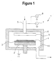
- Fig. 1 is a schematic view of a plasma CVD apparatus usable for a method of manufacturing an interlayer insulation film used for multilayer interconnect of a semiconductor integrated circuit according to an embodiment of the present invention.
- the method of manufacturing an interlayer insulation film used for multilayer interconnect of a semiconductor integrated circuit comprises the following steps: a step of forming a first insulation film by a plasma CVD method using silicon-containing hydrocarbon as a source gas; and a step of forming a second insulation film on the first insulation film in situ by a plasma CVD method using silicon-containing hydrocarbon gas and oxidizing gas as a source gas, consecutively after the first insulation film has been formed.
- a flow rate of the oxidizing gas may be 1.2 to 100 times that of the silicon-containing hydrocarbon gas.
- any suitable one or more silicon-containing hydrocarbon compounds can be used for the first insulation film and/or the second insulation film independently.
- Linear silicon-containing hydrocarbon compounds and/or cyclic silicon-containing hydrocarbon compounds can be used.
- the usable compound may include, but is not limited to, a compound or compounds selected from the group consisting of linear compounds having the formula Si ⁇ O ⁇ -1 R 2 ⁇ - ⁇ +2 (OR) ⁇ wherein ⁇ is an integer of 1-3, ⁇ is 0, 1, or 2, R is C 1-6 saturated hydrocarbon; cyclic compounds having the formula Si n O n R 2n , wherein n is an integer of 3-6, R is C 1-6 saturated hydrocarbon; and cyclic compounds having the formula Si p (C 2 H 2 ) p R 2p , wherein p is an integer of 3-6, and R is C 1-6 saturated or unsaturated hydrocarbon.
- the linear compounds include, but are not limited to, the following compounds: wherein R1, R2, R3, R4, R5, and R6 are each independently C 1-6 saturated or unsaturated hydrocarbon such as CH 3 , C 2 H 3 , C 2 H 5 , C 3 H 7 , C 6 H 5 , C 2 H 3 , C 3 H 5 , C 4 H 7 , and C 4 H 5 .
- a preferable linear silicon-containing hydrocarbon compound has formula: Si ⁇ O ⁇ -1 R 2 ⁇ - ⁇ +2 (OC n H 2n+1 ) ⁇ wherein ⁇ is an integer of 1-3, ⁇ is 0, 1, or 2, n is an integer of 1-3, and R is C 1-6 hydrocarbon attached to Si. In an embodiment, ⁇ is 1 or 2, and ⁇ is 2.
- the source gas may be dimethyl-dimethoxysilane (DM-DMOS), 1,3-dimethoxytetramethyldisiloxan (DMOTMDS) or phenylmethyl dimethoxysilane (PM-DMOS).
- DM-DMOS dimethyl-dimethoxysilane
- DMOTMDS 1,3-dimethoxytetramethyldisiloxan
- PM-DMOS phenylmethyl dimethoxysilane
- Cyclic compounds include, but are not limited to, the following compounds: wherein R1, R2, R3, R4, R5, and R6 are each independently C 1-6 saturated or unsaturated hydrocarbon such as CH 3 , C 2 H 3 , C 2 H 5 , C 3 H 7 , C 6 H 5 , C 3 H 5 , C 4 H 7 , and C 4 H 5 .
- Different source gases can be mixed or a single source gas can be used alone.
- the first insulation film can be formed by any suitable plasma CVD method.
- an additive gas may be used which is selected from the group consisting of a carrier gas, an oxidizing gas, and a plasma stabilizing gas.
- an oxidizing gas may be supplied at a flow rate of 0-100% (including 10%, 20%, 30%, 40%, 50%, 80%, and ranges including any of the forgoing, preferably less than 50%) of that of a silicon-containing hydrocarbon compound.
- the oxygen-supplying gas can be any suitable gas which can supply oxygen and may include O 2 , NO, O 3 , H 2 O 2 , CO 2 , and N 2 O so that oxygen is supplied to adjust a Si/O ratio (e.g., 1:1.3-1:1.7) in the reaction gas or to improve reaction efficacy.
- a Si/O ratio e.g. 1:1.3-1:1.7
- an oxidizing gas may be added to supply oxygen to form a siloxan polymer.
- the carrier gas can be any suitable inert gas including Ar, Ne, He, and N 2 .
- the inert gas may be supplied at a flow rate of 15-300% (50% or more in an embodiment) of that of the source gas.
- the flow rate of additive gas may be 0% to about 500% of the source gas flow (including 10%, 50%, 100%, 200%, 300%, 400%, and ranges including any of the foregoing).
- the reaction gas is excited upstream of the reaction chamber.
- the reaction gas can be excited in a remote plasma chamber installed upstream of a reactor, and the film is deposited on a substrate in the reactor.
- the source gas and the additive gas can be introduced into the remote plasma chamber.
- a reaction space is composed of the interior of the remote plasma chamber, the interior of the reactor, and the interior of the piping connecting the remote plasma chamber and the reactor. Because of using the interior of the remote plasma chamber, the interior of the reactor can be significantly reduced, and thus, the distance between the upper electrode and the lower electrode can be reduced. This leads to not only downsizing the reactor, but also uniformly controlling a plasma over the substrate surface.
- any ,suitable remote plasma chamber and any suitable operation conditions can be used in the present invention.
- usable are the apparatus and the conditions disclosed in U.S. patent applications No. 09/511,934 filed February 24, 2000 and No. 09/764,523 filed January 18, 2001, U.S. patent No. 5,788,778, and U.S. patent No. 5,788,799. The disclosure of each of the above is incorporated herein by reference in its entirety.
- the excitation of the reaction gas may comprise exciting the additive gas and contacting the excited additive gas and the source gas.
- the excitation of the reaction gas can be accomplished in the reactor or upstream of the reactor. As described above, both the source gas and the additive gas can be excited in a remote plasma chamber.
- the excitation of the reaction gas can be accomplished by exciting the additive gas in a remote plasma chamber and mixing it with the source gas downstream of the remote plasma chamber.
- the reaction gas can be heated in a pre-heat chamber installed upstream of a reactor, the reaction gas is excited in the reactor, and film is deposited on the substrate in the reactor.
- the source gas and the additive gas can be introduced into the pre-heater chamber.
- the reaction space is composed of the interior of the pre-heater chamber, the interior of the reactor, and the interior of the piping connecting the pre-heater chamber and the reactor. Because of using the interior of the pre-heater chamber, the interior of the reactor can be significantly reduced, and thus, the distance between the upper electrode and the lower electrode can be reduced. This leads to not only downsizing the reactor, but also uniformly controlling a plasma over the substrate surface.
- Any suitable remote plasma chamber and any suitable operation conditions can be used in the present invention. For example, usable are the apparatus and the conditions disclosed in the aforesaid references.
- the excitation of the reaction gas comprises exciting the additive gas and contacting the excited additive gas and the source gas.
- the additive gas can be excited in a remote plasma chamber, and the source gas is heated in a pre-heater chamber where the excited additive gas and the source gas are in contact, and then the reaction gas flows into the reactor for deposition of a film.
- deposition of unwanted particles on a surface of the remote plasma chamber which causes a failure of ignition or firing, can effectively be avoided, because only the additive gas is present in the remote plasma chamber.
- the source gas is mixed with the excited additive gas downstream of the remote plasma chamber.
- the flow rate of the reaction gas is determined based on the intensity of RF power, the pressure selected for reaction, and the type of source gas and cross-linking gas.
- the reaction pressure is normally in the range of 1-10 Torr, preferably 3-7 Torr, so as to maintain a stable plasma. This reaction pressure is relatively high in order to lengthen the residence time of the reaction gas.
- the total flow of the reaction gas is important for reducing the relative dielectric constant of a resulting film. In general, the longer the residence time, the lower the relative dielectric constant becomes.
- the source gas flow necessary for forming a film depends on the desired deposition rate and the area of a substrate on which a film is formed.
- sccm of the source gas preferably 100-500 sccm, including 150, 200, 250 sccm
- a temperature of the semiconductor wafer may be maintained at a temperature of e.g., 350 to 450°C.
- radio-frequency (RF) power is high-frequency power without low-frequency power.
- high-frequency RF power and low-frequency RF power can be overlaid. That is, a combination of high-frequency power has 2 MHz or higher frequencies (including 5, 10, 15, 20, 25, 30, 40, 50, 60, 70 MHz, and ranges including any of the forgoing) and low-frequency RF power having less than 2 MHz frequencies can be used (the ratio of low-frequency power to high-frequency power may be less than 50% including 40%, 30%, 20%, 10%, 5%, 0%, and ranges including any of the forgoing (preferably, 1%-10%).
- High-frequency RF power may be applied at a high power level such as 1.5 W/cm 2 or higher (including 2.0, 2.25, 2.5, 2.75, 3.0, 3.25, 3.5 W/cm 2 , and ranges including any of the foregoing). Such a high power level can increase the mechanical strength and deposition rate of a resultant insulation film.
- the residence time of a reaction gas may be controlled as disclosed in U.S. patent No. 6,352,945, U.S. patent No. 6,383,955, and U.S. patent No. 6,432,846, all of which are incorporated herein by reference in their entirety.
- the residence time can very more widely than the above.
- Rt may be 50 msec or higher (including 70 msec, 90 msec, 100 msec, 150 msec, 200 msec, 250 msec, and ranges including any of the forgoing).
- the first insulation film may have a dielectric constant of 2.0-3.5, preferably 2.5-3.1, and a hardness of 1.0-6.0 GPa, preferably 1.5-2.5 GPa.
- the film thickness can vary depending on the semiconductor design, and in an embodiment, may be in the range of 0.1-5.0 ⁇ m, preferably 0.3-2.0 ⁇ m.
- the second insulation film can be formed continuously in the reaction chamber.
- the silicon-containing hydrocarbon compound used for the first insulation film can be changed to or can be used in addition to one or more different silicon-containing hydrocarbon compounds for the second insulation film.
- the flow rate of a silicon-containing hydrocarbon compound for the second insulation film may be lower than that used for the first insulation film.
- the flow rate for the second formation may be less than 100%, 80%, 60%, 40%, or 20% of the flow rate for the first formation.
- the flow rate of a silicon-containing hydrocarbon compound for the second formation is 10-1,000 sccm, preferably 50-300 sccm.
- the deposition method, the reaction chamber, and the deposition conditions used for the first film formation may be, but need not be, employed for the second film formation except for those described below, and the second film can be, but need not be, formed continuously in the same reaction chamber.
- an oxidizing gas is indispensable to improve the mechanical strength.
- the oxidizing gas here is used as a part of the source gas, not as a part of an additive gas.
- the oxidizing gas can be the same as or different from those used in the formation of the first insulation film.
- the oxidizing gas may be at least one selected from the group consisting of comprises oxygen, dinitrogenoxide, ozone, hydrogen peroxide, carbon dioxide, and alcohol such as ethylene glycol, 1,2 propanediol, and isopropyl alcohol (IPA), which contributes to formation of Si-O bonds with a silicon-containing hydrocarbon compound in a metric.
- the group consisting of comprises oxygen, dinitrogenoxide, ozone, hydrogen peroxide, carbon dioxide, and alcohol such as ethylene glycol, 1,2 propanediol, and isopropyl alcohol (IPA), which contributes to formation of Si-O bonds with a silicon-containing hydrocarbon compound in a metric.
- IPA isopropyl alcohol
- the flow rate of an oxidizing gas may be more than that of the silicon-containing hydrocarbon compound.
- the ratio of the flow rate of the oxidizing gas to that of the silicon-containing hydrocarbon compound may be 1.0 to 300, preferably 1.2 to 100 (including 1.5, 2, 5, 10, 20, 30, 50, 80, and ranges including any of the forgoing).
- a high flow rate of an oxidizing gas may contribute to a film structure having less Si-C bonds and less C-H bonds, thereby forming a more dense and stable structure. It is expected that the structure is less porous because more Si-O bonds are formed more densely.
- a silicon oxide polymer or oligomer is formed.
- An inert gas and other gases can be added in the range of 0-100% (including 10%, 30%, 50%, 80%, and ranges including any of the forgoing) of the silicon-containing hydrocarbon compound.
- RF power or frequency can be the same as or different from those used in the first formation.
- high power renders mechanical strength of a film high.
- a plasma may become unstablilized. In that case, RF power is reduced.
- high-frequency RF power may be applied at a high power level such as 0.1 W/cm 2 or higher but 3.0 W/cm 2 or lower (including 0.2, 0.5, 1.0, 1.5, 2.0, 2.5 W/cm 2 , and ranges including any of the foregoing).
- the RF power for the second film formation may be lower than 100%, 80%, 50%, or 30% of that for the first film formation.
- a combination of high-frequency RF power and low-frequency RF power can be used.
- higher RF power is generally preferable, suitable RF power can vary depending the flow rate of an oxidizing gas and the flow rate of an silicon-containing hydrocarbon compound, etc.
- the reaction pressure for the second film formation is normally in the range of 0.1-10 Torr, preferably 0.5-5 Torr (including 0.75, 1, 2, 3, and ranges including any of the forgoing), so as to maintain a stable plasma even though the flow rate of an oxidizing gas is high.
- the reaction pressure for the second film formation may be lower than that for the first film formation. When the reaction pressure is too low or too high, the uniformity of film thickness may suffer.
- the second insulation film has a dielectric constant of 3.0-5.0, preferably 3.5-3.9, and a hardness of 6 GPa or higher, preferably 6-15 GPa.
- the film thickness can vary depending on the semiconductor design, and in an embodiment, may be in the range of 0.01-0.5 ⁇ m, preferably 0.03-0.15 ⁇ m.
- the second insulation film may not be uniform in a vertical direction. That is, in an embodiment, the second insulation film may have a gradient hardness in the vertical direction. The outmost surface of the second insulation film may be hardest and the boundary surface with the first insulation film may be as hard as the first insulation film.
- the flow rate of an oxidizing gas (and/or the reason pressure, the RF power and frequency, the flow rate of an silicon-containing hydrocarbon compound, etc.) may gradually increase at a certain rate, so that the oxygen concentration increases and the carbon concentration decreases toward the outmost surface of the second insulation film. In an embodiment, the closer the distance to the outmost surface of the second insulation film, the higher the mechanical strength becomes.
- the second insulation film is composed of multiple layers or films each having a different hardness, wherein the closer the distance to the outmost surface of the second insulation film, the higher the mechanical strength becomes.
- Fig. 1 is a schematic view of plasma CVD equipment useable for a method of manufacturing an interlayer insulation film used for multilayer interconnect of a semiconductor integrated circuit according to an embodiment of the present invention.
- the plasma CVD equipment 1 includes a reaction chamber 6. Inside the reaction chamber 6, a susceptor 3 holding a semiconductor wafer 4 thereon is set up. The susceptor 3 is supported by a heater 2; the heater 2 maintains the semiconductor wafer 4 at a given temperature (e.g., 350 to 450°C). The susceptor 3 also serves as one electrode for plasma discharge as well and is grounded 11 through the reaction chamber 6. On the ceiling inside the reaction chamber 6, a shower head 9 is set up in parallel and opposing to the susceptor 3. The shower head 9 has many fine pores in its bottom, from which a jet of source gases described later is emitted to the semiconductor wafer 4.
- a source gas inlet port 5 is provided; the source gases are brought into the shower head 9 via a gas line (not shown).
- the gas inlet port 5 is electrically insulated from the reaction chamber 6.
- the shower head 9 also serves as the other electrode for plasma discharge and is connected to the first high-frequency power source 7 and the second high-frequency power source 8 via source gas inlet port 5.
- a plasma reaction zone is generated in the vicinity of the semiconductor wafer 4.
- an exhaust port 10 is provided and is connected to an external vacuum pump (not shown).
- the method of manufacturing an interlayer insulation film used for multilayer interconnect of a semiconductor integrated circuit according to an embodiment of the present invention includes a step of forming a first insulation film by the plasma CVD method using silicon-containing hydrocarbon as a source gas.
- the source gas here is silicon-containing hydrocarbon which is expressed by a general formula: Si ⁇ O ⁇ -1 (R) 2 ⁇ - ⁇ +2 (OC n H 2n+1 ) ⁇ (where ⁇ is an integer of 1-3; ⁇ is an integer of 0-2; n is an integer of 1-3, and R is C 1-6 hydrocarbon attached to Si) and is preferably DM-DMOS (dimethy-dimethoxysilane).
- a sub-source gas CO 2 , alcohol, hydrocarbon which contains at least one unsaturated bond, or N 2 can be contained. If a Si/O ratio needs to be controlled, O 2 or N 2 O can also be added as a sub-source gas. Additionally, as an added gas, inert gases such as Ar and/or He can also be added in.
- the source gas is brought into the reaction chamber 6 from the gas inlet port 5 through the shower head 9. Subsequently, high-frequency power for plasma excitation is applied from the first high-frequency power source 7 and the second high-frequency power source 8, and a plasma reaction zone is formed in the vicinity of the semiconductor wafer 4.
- a frequency of the first high-frequency power source 7 here is above 2MHz, and a frequency of the second high-frequency power source 8 to be overlapped is below 2MHz.
- Source gas atoms which are decomposed in the plasma react chemically, and the first insulation film containing SixCyOz is deposited on the semiconductor wafer 4.
- the method of manufacturing an interlayer insulation film used for multilayer interconnect includes a step of forming a second insulation film on the first insulation film by a plasma CVD method using silicon-containing hydrocarbon and oxidizing gas as a source gas.
- the plasma CVD method for the second insulation film can be the same as or different from the plasma CVD method for the first insulation film.
- the second insulation film can be formed in another reaction chamber.
- the silicon-containing hydrocarbon used as a source gas here is silicon-containing hydrocarbon which is expressed by a general formula: Si ⁇ O ⁇ -1 R 2 ⁇ - ⁇ +2 (OC n H 2n+1 ) ⁇ (where ⁇ is an integer of 1-3; ⁇ is an integer of 0-2; n is an integer of 1-3, and R is C 1-6 hydrocarbon attached to Si) and is preferably DM-DMOS (dimethy-dimethoxysilane).
- the oxidizing gas used as a source gas comprises at least one of oxygen, dinitrogenoxide, ozone, hydrogen peroxide, carbon dioxide, or alcohol.
- the resulting second insulation film possesses high mechanical strength and serves as a polishing stopper film.
- source gases are brought into the reaction chamber 6 from the gas inlet port 5 in situ and consecutively.
- a flow rate of oxidizing gas may be controlled 1.2 to 100 times as much as a flow rate of the silicon-containing hydrocarbon, for example.
- high-frequency power for plasma excitation is applied from the first high-frequency power source 7 and the second high-frequency power source 8, and a plasma reaction zone is formed in the vicinity of the semiconductor wafer 4.
- a frequency of the first high-frequency power source 7 here is above 2MHz and a frequency of the second high-frequency power source 8 to be overlapped is below 2MHz.
- Source gas atoms which are decomposed in the plasma react chemically, and the second insulation film containing SiO 2 is deposited on the semiconductor wafer 4.
- a characteristic of the first insulation film is that it has a low dielectric constant. This is because Si-C bonds in the main source gas (silicon-containing hydrocarbon) are incorporated in the film as they are; hence, the density of the film becomes nondense.
- the first insulation film has a shortcoming of low mechanical strength because it contains many -CHx bonds in the film and is porous. Focusing attention on this particular aspect, the inventors of the present invention have reached to invent a method of forming the second insulation film having high mechanical strength on the first insulation film to cover the shortcoming of the first insulation film.
- a characteristic of the second insulation film is that it has high mechanical strength. It is thought that the film becomes dense because C is not incorporated in the film by excessively feeding the oxidizing gas.
- the first insulation film of 1 ⁇ m was formed using the above-mentioned system and deposition conditions. After that, the second insulation film of 0.1 ⁇ m was formed in situ according to the deposition conditions shown in Table 1 continuously. After the CMP was performed on the Damascene structure fabricated, no dishing was detected under all conditions shown in Table 1.
- an insulation film functioning as a polishing stopper is able to be provided.
- the dishing problem of a SixCyOz film, a low- k insulation film can effectively be solved.
- the present invention includes, but is not limited to, the following embodiments:
Landscapes
- Chemical & Material Sciences (AREA)
- General Chemical & Material Sciences (AREA)
- Chemical Kinetics & Catalysis (AREA)
- Engineering & Computer Science (AREA)
- Materials Engineering (AREA)
- Mechanical Engineering (AREA)
- Metallurgy (AREA)
- Organic Chemistry (AREA)
- Inorganic Chemistry (AREA)
- Internal Circuitry In Semiconductor Integrated Circuit Devices (AREA)
- Formation Of Insulating Films (AREA)
Applications Claiming Priority (2)
| Application Number | Priority Date | Filing Date | Title |
|---|---|---|---|
| JP2002262304A JP4015510B2 (ja) | 2002-09-09 | 2002-09-09 | 半導体集積回路の多層配線用層間絶縁膜及びその製造方法 |
| JP2002262304 | 2002-09-09 |
Publications (2)
| Publication Number | Publication Date |
|---|---|
| EP1396884A2 true EP1396884A2 (fr) | 2004-03-10 |
| EP1396884A3 EP1396884A3 (fr) | 2005-07-06 |
Family
ID=31712354
Family Applications (1)
| Application Number | Title | Priority Date | Filing Date |
|---|---|---|---|
| EP03020250A Withdrawn EP1396884A3 (fr) | 2002-09-09 | 2003-09-08 | Couche isolante intermédiaire pour un circuit multicouche interconnecté et procédé de fabrication |
Country Status (4)
| Country | Link |
|---|---|
| US (1) | US7098129B2 (fr) |
| EP (1) | EP1396884A3 (fr) |
| JP (1) | JP4015510B2 (fr) |
| KR (1) | KR20040023557A (fr) |
Cited By (1)
| Publication number | Priority date | Publication date | Assignee | Title |
|---|---|---|---|---|
| EP1342809A1 (fr) * | 2002-03-04 | 2003-09-10 | Asm Japan K.K. | Procédé de production d'un film isolant à faible constante diélectrique |
Families Citing this family (15)
| Publication number | Priority date | Publication date | Assignee | Title |
|---|---|---|---|---|
| US7582575B2 (en) * | 1998-02-05 | 2009-09-01 | Asm Japan K.K. | Method for forming insulation film |
| JP4917249B2 (ja) * | 2004-02-03 | 2012-04-18 | ルネサスエレクトロニクス株式会社 | 半導体装置及び半導体装置の製造方法 |
| US7030041B2 (en) * | 2004-03-15 | 2006-04-18 | Applied Materials Inc. | Adhesion improvement for low k dielectrics |
| KR100648632B1 (ko) * | 2005-01-25 | 2006-11-23 | 삼성전자주식회사 | 높은 유전율을 갖는 유전체 구조물의 제조 방법 및 이를 포함하는 반도체 소자의 제조 방법 |
| US7189658B2 (en) * | 2005-05-04 | 2007-03-13 | Applied Materials, Inc. | Strengthening the interface between dielectric layers and barrier layers with an oxide layer of varying composition profile |
| KR100791334B1 (ko) * | 2006-07-26 | 2008-01-07 | 삼성전자주식회사 | 원자층 증착법을 이용한 금속 산화막 형성 방법 |
| TWI595691B (zh) * | 2010-07-28 | 2017-08-11 | 應用材料股份有限公司 | 用於磁性媒材圖案化之阻劑強化 |
| WO2012028721A1 (fr) | 2010-09-03 | 2012-03-08 | Sandoz Ag | Procédé d'amination réductrice d'acides α-céto-carboxyliques |
| US9589799B2 (en) * | 2013-09-30 | 2017-03-07 | Lam Research Corporation | High selectivity and low stress carbon hardmask by pulsed low frequency RF power |
| WO2020190441A1 (fr) * | 2019-03-19 | 2020-09-24 | Applied Materials, Inc. | Revêtement hydrophobe et glaciophobe |
| CN113891954B (zh) | 2019-05-29 | 2025-09-19 | 朗姆研究公司 | 通过高功率脉冲低频率rf产生的高选择性、低应力、且低氢的类金刚石碳硬掩模 |
| CN114342043A (zh) | 2019-08-30 | 2022-04-12 | 朗姆研究公司 | 低压下的高密度、模量和硬度的非晶碳膜 |
| TW202229612A (zh) | 2020-10-06 | 2022-08-01 | 荷蘭商Asm Ip私人控股有限公司 | 在部件的側壁上形成氮化矽的方法及系統 |
| US20230386825A1 (en) * | 2020-10-20 | 2023-11-30 | Versum Materials Us, Llc | Alkoxydisiloxanes and dense organosilica films made therefrom |
| US20240110284A1 (en) * | 2022-09-30 | 2024-04-04 | Applied Materials, Inc. | Selective Deposition of Thin Films with Improved Stability |
Family Cites Families (17)
| Publication number | Priority date | Publication date | Assignee | Title |
|---|---|---|---|---|
| JP3979687B2 (ja) | 1995-10-26 | 2007-09-19 | アプライド マテリアルズ インコーポレイテッド | ハロゲンをドープした酸化珪素膜の膜安定性を改良する方法 |
| US6599847B1 (en) * | 1996-08-27 | 2003-07-29 | Taiwan Semiconductor Manufacturing Company | Sandwich composite dielectric layer yielding improved integrated circuit device reliability |
| US6593247B1 (en) * | 1998-02-11 | 2003-07-15 | Applied Materials, Inc. | Method of depositing low k films using an oxidizing plasma |
| US6068884A (en) | 1998-04-28 | 2000-05-30 | Silcon Valley Group Thermal Systems, Llc | Method of making low κ dielectric inorganic/organic hybrid films |
| US6165898A (en) * | 1998-10-23 | 2000-12-26 | Taiwan Semiconductor Manufacturing Company | Dual damascene patterned conductor layer formation method without etch stop layer |
| DE60037395T2 (de) * | 1999-03-09 | 2008-11-27 | Tokyo Electron Ltd. | Herstellung eines halbleiter-bauelementes |
| US6383917B1 (en) | 1999-10-21 | 2002-05-07 | Intel Corporation | Method for making integrated circuits |
| US6902771B2 (en) | 2000-02-01 | 2005-06-07 | Jsr Corporation | Process for producing silica-based film, silica-based film, insulating film, and semiconductor device |
| CN1432035A (zh) | 2000-06-06 | 2003-07-23 | 陶氏化学公司 | 用于聚合物与容器的阻隔层 |
| JP4689027B2 (ja) | 2000-10-23 | 2011-05-25 | 株式会社Sumco | 半導体単結晶引上装置 |
| US6531398B1 (en) * | 2000-10-30 | 2003-03-11 | Applied Materials, Inc. | Method of depositing organosillicate layers |
| US6936533B2 (en) * | 2000-12-08 | 2005-08-30 | Samsung Electronics, Co., Ltd. | Method of fabricating semiconductor devices having low dielectric interlayer insulation layer |
| US6713382B1 (en) * | 2001-01-31 | 2004-03-30 | Advanced Micro Devices, Inc. | Vapor treatment for repairing damage of low-k dielectric |
| US6762127B2 (en) * | 2001-08-23 | 2004-07-13 | Yves Pierre Boiteux | Etch process for dielectric materials comprising oxidized organo silane materials |
| US6887780B2 (en) | 2001-08-31 | 2005-05-03 | Intel Corporation | Concentration graded carbon doped oxide |
| US6602779B1 (en) * | 2002-05-13 | 2003-08-05 | Taiwan Semiconductor Manufacturing Co., Ltd | Method for forming low dielectric constant damascene structure while employing carbon doped silicon oxide planarizing stop layer |
| US7186640B2 (en) * | 2002-06-20 | 2007-03-06 | Chartered Semiconductor Manufacturing Ltd. | Silicon-rich oxide for copper damascene interconnect incorporating low dielectric constant dielectrics |
-
2002
- 2002-09-09 JP JP2002262304A patent/JP4015510B2/ja not_active Expired - Lifetime
-
2003
- 2003-09-08 US US10/657,416 patent/US7098129B2/en not_active Expired - Lifetime
- 2003-09-08 EP EP03020250A patent/EP1396884A3/fr not_active Withdrawn
- 2003-09-09 KR KR1020030063098A patent/KR20040023557A/ko not_active Withdrawn
Cited By (1)
| Publication number | Priority date | Publication date | Assignee | Title |
|---|---|---|---|---|
| EP1342809A1 (fr) * | 2002-03-04 | 2003-09-10 | Asm Japan K.K. | Procédé de production d'un film isolant à faible constante diélectrique |
Also Published As
| Publication number | Publication date |
|---|---|
| US20040048490A1 (en) | 2004-03-11 |
| EP1396884A3 (fr) | 2005-07-06 |
| JP4015510B2 (ja) | 2007-11-28 |
| US7098129B2 (en) | 2006-08-29 |
| KR20040023557A (ko) | 2004-03-18 |
| JP2004103752A (ja) | 2004-04-02 |
Similar Documents
| Publication | Publication Date | Title |
|---|---|---|
| US7354873B2 (en) | Method for forming insulation film | |
| US6340843B1 (en) | Plasma CVD dielectric film and process for forming the same | |
| US7582575B2 (en) | Method for forming insulation film | |
| US7718553B2 (en) | Method for forming insulation film having high density | |
| US7098129B2 (en) | Interlayer insulation film used for multilayer interconnect of semiconductor integrated circuit and method of manufacturing the same | |
| KR100404536B1 (ko) | 유전 상수 κ가 낮은 무기/유기 혼성 박막 및 이를제조하는 방법 | |
| US6740602B1 (en) | Method of forming low-dielectric constant film on semiconductor substrate by plasma reaction using high-RF power | |
| US6410463B1 (en) | Method for forming film with low dielectric constant on semiconductor substrate | |
| US7312524B2 (en) | Method for fabricating an ultralow dielectric constant material as an intralevel or interlevel dielectric in a semiconductor device and electronic device made | |
| US6514880B2 (en) | Siloxan polymer film on semiconductor substrate and method for forming same | |
| US6991959B2 (en) | Method of manufacturing silicon carbide film | |
| US7064088B2 (en) | Method for forming low-k hard film | |
| CN101495674B (zh) | 多孔质绝缘膜的形成方法 | |
| EP1342809A1 (fr) | Procédé de production d'un film isolant à faible constante diélectrique | |
| KR102827738B1 (ko) | 로우-κ 유전체 막들을 증착하기 위한 시스템들 및 방법들 | |
| KR20020070436A (ko) | 무기/유기 유전체 막의 증착 시스템 및 증착 방법 | |
| US20060258176A1 (en) | Method for forming insulation film | |
| JPH1154504A (ja) | 積層絶縁体膜の形成方法およびこれを用いた半導体装置 | |
| US7148154B2 (en) | Method of forming silicon-containing insulation film having low dielectric constant and low film stress | |
| TWI831824B (zh) | 非uv高硬度低介電常數膜沉積 | |
| US6905978B2 (en) | Method of forming interlayer insulation film | |
| JP2002305242A (ja) | 半導体装置の製造方法 | |
| JP2006294671A (ja) | 低誘電率炭化珪素膜の製造方法 |
Legal Events
| Date | Code | Title | Description |
|---|---|---|---|
| PUAI | Public reference made under article 153(3) epc to a published international application that has entered the european phase |
Free format text: ORIGINAL CODE: 0009012 |
|
| AK | Designated contracting states |
Kind code of ref document: A2 Designated state(s): AT BE BG CH CY CZ DE DK EE ES FI FR GB GR HU IE IT LI LU MC NL PT RO SE SI SK TR |
|
| AX | Request for extension of the european patent |
Extension state: AL LT LV MK |
|
| PUAL | Search report despatched |
Free format text: ORIGINAL CODE: 0009013 |
|
| AK | Designated contracting states |
Kind code of ref document: A3 Designated state(s): AT BE BG CH CY CZ DE DK EE ES FI FR GB GR HU IE IT LI LU MC NL PT RO SE SI SK TR |
|
| AX | Request for extension of the european patent |
Extension state: AL LT LV MK |
|
| RIC1 | Information provided on ipc code assigned before grant |
Ipc: 7H 01L 21/321 B Ipc: 7C 23C 16/56 B Ipc: 7C 23C 16/30 B Ipc: 7H 01L 21/768 B Ipc: 7H 01L 21/316 A |
|
| 17P | Request for examination filed |
Effective date: 20051223 |
|
| AKX | Designation fees paid |
Designated state(s): DE FR GB |
|
| 17Q | First examination report despatched |
Effective date: 20060207 |
|
| STAA | Information on the status of an ep patent application or granted ep patent |
Free format text: STATUS: THE APPLICATION IS DEEMED TO BE WITHDRAWN |
|
| 18D | Application deemed to be withdrawn |
Effective date: 20080401 |