EP1399262B1 - Pipettenvorrichtung und verfahren zu deren herstellung - Google Patents
Pipettenvorrichtung und verfahren zu deren herstellung Download PDFInfo
- Publication number
- EP1399262B1 EP1399262B1 EP02754726A EP02754726A EP1399262B1 EP 1399262 B1 EP1399262 B1 EP 1399262B1 EP 02754726 A EP02754726 A EP 02754726A EP 02754726 A EP02754726 A EP 02754726A EP 1399262 B1 EP1399262 B1 EP 1399262B1
- Authority
- EP
- European Patent Office
- Prior art keywords
- substrate
- hole
- rim
- pipette
- surface layer
- Prior art date
- Legal status (The legal status is an assumption and is not a legal conclusion. Google has not performed a legal analysis and makes no representation as to the accuracy of the status listed.)
- Expired - Lifetime
Links
- 238000004519 manufacturing process Methods 0.000 title description 10
- 239000000758 substrate Substances 0.000 claims abstract description 127
- 238000000034 method Methods 0.000 claims description 68
- 239000002344 surface layer Substances 0.000 claims description 51
- 239000000463 material Substances 0.000 claims description 49
- 239000010410 layer Substances 0.000 claims description 35
- 230000008569 process Effects 0.000 claims description 35
- 229910052710 silicon Inorganic materials 0.000 claims description 19
- 238000005530 etching Methods 0.000 claims description 17
- 239000010703 silicon Substances 0.000 claims description 17
- 239000011248 coating agent Substances 0.000 claims description 12
- 238000000576 coating method Methods 0.000 claims description 12
- VYPSYNLAJGMNEJ-UHFFFAOYSA-N Silicium dioxide Chemical compound O=[Si]=O VYPSYNLAJGMNEJ-UHFFFAOYSA-N 0.000 claims description 9
- 239000004065 semiconductor Substances 0.000 claims description 9
- 230000015572 biosynthetic process Effects 0.000 claims description 7
- 238000005121 nitriding Methods 0.000 claims description 7
- 239000000126 substance Substances 0.000 claims description 7
- 230000004048 modification Effects 0.000 claims description 3
- 238000012986 modification Methods 0.000 claims description 3
- 230000003647 oxidation Effects 0.000 claims description 3
- 238000007254 oxidation reaction Methods 0.000 claims description 3
- 239000000377 silicon dioxide Substances 0.000 claims description 3
- 239000004020 conductor Substances 0.000 claims description 2
- 230000003628 erosive effect Effects 0.000 claims 3
- 229910052581 Si3N4 Inorganic materials 0.000 claims 2
- 229910052681 coesite Inorganic materials 0.000 claims 2
- 229910052906 cristobalite Inorganic materials 0.000 claims 2
- 229910052682 stishovite Inorganic materials 0.000 claims 2
- 229910052905 tridymite Inorganic materials 0.000 claims 2
- 239000003795 chemical substances by application Substances 0.000 claims 1
- 239000007788 liquid Substances 0.000 description 16
- XUIMIQQOPSSXEZ-UHFFFAOYSA-N Silicon Chemical compound [Si] XUIMIQQOPSSXEZ-UHFFFAOYSA-N 0.000 description 14
- 210000004027 cell Anatomy 0.000 description 9
- 239000011521 glass Substances 0.000 description 9
- 229910004298 SiO 2 Inorganic materials 0.000 description 5
- 239000011148 porous material Substances 0.000 description 5
- 238000007639 printing Methods 0.000 description 5
- 238000003786 synthesis reaction Methods 0.000 description 5
- 238000012549 training Methods 0.000 description 5
- 238000000018 DNA microarray Methods 0.000 description 4
- 229910052782 aluminium Inorganic materials 0.000 description 4
- 239000012528 membrane Substances 0.000 description 4
- 230000001590 oxidative effect Effects 0.000 description 4
- 238000005498 polishing Methods 0.000 description 4
- 238000003491 array Methods 0.000 description 3
- 230000008901 benefit Effects 0.000 description 3
- 238000005516 engineering process Methods 0.000 description 3
- 150000002632 lipids Chemical class 0.000 description 3
- 229910018072 Al 2 O 3 Inorganic materials 0.000 description 2
- 229910010413 TiO 2 Inorganic materials 0.000 description 2
- XAGFODPZIPBFFR-UHFFFAOYSA-N aluminium Chemical compound [Al] XAGFODPZIPBFFR-UHFFFAOYSA-N 0.000 description 2
- 210000000170 cell membrane Anatomy 0.000 description 2
- 230000001419 dependent effect Effects 0.000 description 2
- 230000000694 effects Effects 0.000 description 2
- 230000005484 gravity Effects 0.000 description 2
- 229910052735 hafnium Inorganic materials 0.000 description 2
- AMGQUBHHOARCQH-UHFFFAOYSA-N indium;oxotin Chemical compound [In].[Sn]=O AMGQUBHHOARCQH-UHFFFAOYSA-N 0.000 description 2
- 229910052751 metal Inorganic materials 0.000 description 2
- 239000002184 metal Substances 0.000 description 2
- 239000000203 mixture Substances 0.000 description 2
- 150000004767 nitrides Chemical class 0.000 description 2
- 238000007789 sealing Methods 0.000 description 2
- 238000012546 transfer Methods 0.000 description 2
- 206010013710 Drug interaction Diseases 0.000 description 1
- 229910001218 Gallium arsenide Inorganic materials 0.000 description 1
- 102000004310 Ion Channels Human genes 0.000 description 1
- 239000000232 Lipid Bilayer Substances 0.000 description 1
- 239000000020 Nitrocellulose Substances 0.000 description 1
- 230000009471 action Effects 0.000 description 1
- 238000003556 assay Methods 0.000 description 1
- 239000012298 atmosphere Substances 0.000 description 1
- QVGXLLKOCUKJST-UHFFFAOYSA-N atomic oxygen Chemical compound [O] QVGXLLKOCUKJST-UHFFFAOYSA-N 0.000 description 1
- 230000009286 beneficial effect Effects 0.000 description 1
- 230000008859 change Effects 0.000 description 1
- 238000005520 cutting process Methods 0.000 description 1
- 210000000805 cytoplasm Anatomy 0.000 description 1
- 230000003247 decreasing effect Effects 0.000 description 1
- 238000013461 design Methods 0.000 description 1
- 238000003795 desorption Methods 0.000 description 1
- 230000009881 electrostatic interaction Effects 0.000 description 1
- 210000003743 erythrocyte Anatomy 0.000 description 1
- 229910052732 germanium Inorganic materials 0.000 description 1
- GNPVGFCGXDBREM-UHFFFAOYSA-N germanium atom Chemical compound [Ge] GNPVGFCGXDBREM-UHFFFAOYSA-N 0.000 description 1
- 238000010438 heat treatment Methods 0.000 description 1
- 238000005286 illumination Methods 0.000 description 1
- 239000012535 impurity Substances 0.000 description 1
- 238000011005 laboratory method Methods 0.000 description 1
- 239000007791 liquid phase Substances 0.000 description 1
- 239000011159 matrix material Substances 0.000 description 1
- 230000008018 melting Effects 0.000 description 1
- 238000002844 melting Methods 0.000 description 1
- 210000002569 neuron Anatomy 0.000 description 1
- 229920001220 nitrocellulos Polymers 0.000 description 1
- 239000012299 nitrogen atmosphere Substances 0.000 description 1
- 239000013307 optical fiber Substances 0.000 description 1
- 239000011368 organic material Substances 0.000 description 1
- TWNQGVIAIRXVLR-UHFFFAOYSA-N oxo(oxoalumanyloxy)alumane Chemical compound O=[Al]O[Al]=O TWNQGVIAIRXVLR-UHFFFAOYSA-N 0.000 description 1
- 239000001301 oxygen Substances 0.000 description 1
- 229910052760 oxygen Inorganic materials 0.000 description 1
- 230000003071 parasitic effect Effects 0.000 description 1
- 239000002245 particle Substances 0.000 description 1
- 238000012402 patch clamp technique Methods 0.000 description 1
- 229920001296 polysiloxane Polymers 0.000 description 1
- 229910021426 porous silicon Inorganic materials 0.000 description 1
- 238000012545 processing Methods 0.000 description 1
- 230000009467 reduction Effects 0.000 description 1
- 230000001105 regulatory effect Effects 0.000 description 1
- 150000004760 silicates Chemical class 0.000 description 1
- 150000003376 silicon Chemical class 0.000 description 1
- 235000012239 silicon dioxide Nutrition 0.000 description 1
- 229910052814 silicon oxide Inorganic materials 0.000 description 1
- 239000002356 single layer Substances 0.000 description 1
- 229920002994 synthetic fiber Polymers 0.000 description 1
- 230000001960 triggered effect Effects 0.000 description 1
- 238000011144 upstream manufacturing Methods 0.000 description 1
- 238000007740 vapor deposition Methods 0.000 description 1
- XLYOFNOQVPJJNP-UHFFFAOYSA-N water Substances O XLYOFNOQVPJJNP-UHFFFAOYSA-N 0.000 description 1
Images

Classifications
-
- B—PERFORMING OPERATIONS; TRANSPORTING
- B81—MICROSTRUCTURAL TECHNOLOGY
- B81C—PROCESSES OR APPARATUS SPECIALLY ADAPTED FOR THE MANUFACTURE OR TREATMENT OF MICROSTRUCTURAL DEVICES OR SYSTEMS
- B81C1/00—Manufacture or treatment of devices or systems in or on a substrate
- B81C1/00015—Manufacture or treatment of devices or systems in or on a substrate for manufacturing microsystems
- B81C1/00023—Manufacture or treatment of devices or systems in or on a substrate for manufacturing microsystems without movable or flexible elements
- B81C1/00087—Holes
-
- B—PERFORMING OPERATIONS; TRANSPORTING
- B01—PHYSICAL OR CHEMICAL PROCESSES OR APPARATUS IN GENERAL
- B01L—CHEMICAL OR PHYSICAL LABORATORY APPARATUS FOR GENERAL USE
- B01L3/00—Containers or dishes for laboratory use, e.g. laboratory glassware; Droppers
- B01L3/02—Burettes; Pipettes
- B01L3/0241—Drop counters; Drop formers
-
- B—PERFORMING OPERATIONS; TRANSPORTING
- B81—MICROSTRUCTURAL TECHNOLOGY
- B81B—MICROSTRUCTURAL DEVICES OR SYSTEMS, e.g. MICROMECHANICAL DEVICES
- B81B2201/00—Specific applications of microelectromechanical systems
- B81B2201/05—Microfluidics
- B81B2201/057—Micropipets, dropformers
Definitions
- the invention relates to a device, in particular for a Patch clamping of vesicles and / or for dispensing small, defined amounts of liquid on surfaces as well a method for forming at least one pipette in one Substrate.
- Such Printheads are designed to parallel a large number well-defined, smallest amounts of liquid with large Position accuracy at predetermined spot positions to be able to reproducibly apply to a surface.
- the Spot distances are typically in areas between 10 ⁇ m and 1000 ⁇ m.
- dispensing quantities is one high uniformity and reproducibility of the printing process required over the substrate.
- the state of the art Known printheads only meet this requirement profile conditionally.
- the invention is also advantageous in that of Neher and Sackmann invented patch clamp technology, which for many years to the central laboratory methods in many Heard of areas of cell biology.
- patch clamp technique With the patch clamp technique becomes a relatively large and good at the same time sealed access to a vesicle or cell created, which on the one hand allows the composition of the cytoplasm, and on the other hand one low impedance electrical access with very little Leakage conductivity represents.
- a patch clamp one extremely tight connection of the ring-shaped tip of a Glass micropipette with a cell membrane reached.
- the seal is characterized by the electrical Ring contact resistance. This resistance lies preferably in the Gigaohm range, i.e. it is a so-called "Giga Seal”.
- the patch pipettes used for patch clamping are listed under mechanical pull and heat from a glass tube manufactured. This process is relatively complex and difficult to control. Furthermore, the handling of such individuals Patch pipettes very complex, because a positioning and Holding accuracy in the sub- ⁇ m range must be achieved. To are very complex micromanipulators required, which have a high rigidity and must be constructed and stored with very little vibration. Such systems are very expensive and also very expensive large, so that no more than three to four pipettes can be used simultaneously.
- Another problem is the stray capacity of the pipette whose wall in the area of the tip is approximately a thickness from 200 nm to 300 nm.
- the wall thickness is often one Patch pipette by manual application of silicone to almost raised to the top.
- the device according to the invention is particularly suitable for patch clamping of vesicles.
- vesicles are here Objects, especially biological objects from one closed lipid membrane understood, which in liquid Phase, preferably water, are manageable. Are general this is particles that have a lipid membrane with at least one Include lipid layer.
- lipid membrane with at least one Include lipid layer.
- vesicles are Cells, especially nerve cells, are genetically engineered Cells with voltage-dependent ion channels, from erythrocytes fused giant cells or spheres out Lipid bilayers.
- the device according to the invention is suitable for well-defined, reproducible application ('printing') smallest amounts of liquid in the pico to nanoliter range on a surface.
- 'printing' is a key factor in the production of biochips Process.
- the device according to the invention is in a substrate at least one pipette in the form of a through hole a predetermined diameter, with an edge of the through hole by a predetermined amount of one protrudes adjacent surface of the substrate.
- This protruding edge forms a pipette tip similar to that Tip of a conventional patch pipette.
- the pipette with the protruding edge can also in Form of a particularly split pressure needle or nozzle or -capillary be formed so that the Device according to the invention is suitable as a 'printhead'.
- the edge can according to the desired geometric shape Pipette tip are formed so that on or with it in particular optimal patch clamping or optimal Liquid transfer properties can be achieved.
- the Diameter of the through hole is in the area of the edge, which forms the pipette tip, preferably in the area from 0.5 to 20 ⁇ m, more preferably 1 to 2 ⁇ m.
- the arrangement of such a pipette in a substrate or Carrier enables high mechanical stability, so that elaborate micromanipulators can be dispensed with.
- the substrate is preferably planar or flat.
- the individual vesicles or Cells on this in the area of the pipette tip or On the edge. You can also do this at the Positioning aids for vesicles arranged be so that a vesicle is precisely aligned on the Pipette tip can be placed.
- the substrate that can Through hole i.e. the pipette at a precisely defined one Position are formed so that later a very easy and automatic arrangement of a vesicle is possible.
- the pipette When using the device according to the invention as Printhead can pinch or tear off of the Drops of liquid to be dispensed over the pipette special geometry of the protruding edges controlled become.
- the shape of these edges is free in many areas selectable. In particular, are tapered, straight or funnel-shaped edge geometries possible.
- the pipette at its edge or opening area in particular the edge thickness, edge height and local edge curvature, can be a exact matching of the pipette shape to the desired one Pinch-off or tear-off behavior can be achieved.
- the opening geometry of the pipette In a cutting surface perpendicular to the pipette's longitudinal axis the opening geometry of the pipette can be particularly round, be rectangular or slit-shaped.
- the Tilt angle (opening angle) of the protruding walls or Margins can be varied over a wide range. hereby a high level of uniformity of the printing or Dispensing process with a device according to the invention reached over the substrate to be printed, whereby reproducibly smallest dispensing quantities in the pico to Have the nanoliter range set.
- At least the edge preferably comprises at least one other material than the substrate and preferably SiO 2 or Si 3 N 4 .
- the edge can also have Ta 2 O 5 , HfO 2 , Y 2 O 3 , Al 2 O 3 , Nb 2 O 5 , TiO 2 , TaO 2 and / or nitride or oxynitride of Al, Si or Hf.
- Patch clamp of vesicles can preferably be made from a rim Be formed material which is essentially that is similar to a conventional patch pipette made of glass similarly good sealing properties to a vesicle membrane guarantee.
- the material of the edge i.e. the Pipette tip, which comes into contact with a vesicle, in the essentially independent of the material of the substrate to get voted.
- the material of the substrate can be mechanical points of view to be selected greatest possible stability or rigidity of the device to reach.
- the thickness of the edge is preferably in the range from 200 to 300 nm and thus corresponds in particular to that Wall thickness of conventional patch pipettes ..
- an inner wall of the through hole consists at least partially of a different material than the substrate and preferably of SiO 2 or Si 3 N 4 .
- the inner wall can also have Ta 2 O 5 , HfO 2 , Y 2 O 3 , Al 2 O 3 , Nb 2 O 5 , TiO 2 , TaO 2 and / or nitride or oxynitride of Al, Si or Hf.
- the inner wall of the through hole can be formed in one piece from the same material as the edge.
- Such a configuration essentially forms a pipette integrated in a substrate, which has an inner surface with the desired material properties.
- the coating or the material of the inner wall of the through hole can be selected in particular in accordance with electrical requirements in order to ensure the lowest possible stray capacity of the pipette in the case of a patch clamp.
- the thickness of the coating can be set as desired, but is preferably in the range from 200 to 300 nm.
- the inside of the rim and preferably the inside of the Through hole can preferably be made of a different material exist as the outside of the edge.
- the arrangement of the edge is thus at least two layers trained so that the properties of the pipette outside regardless of the properties of the inner pipette wall can be adjusted.
- the inner wall the through hole made of the same material as the edge i.e. is integrally formed with this, can preferably also the inner wall of the through hole correspondingly at least from two different ones Material layers can be formed.
- Is preferred on the edge and / or on the inner wall of the Through hole at least one layer of an electrical conductive material.
- the Edge and the coating on the inner wall of the Through hole constructed in three layers.
- Have to Example the two outer ones, that is, the one facing the hole and the layer facing the substrate is electrical insulating properties, while the middle layer of is of an electrically conductive nature.
- This middle layer can for example from a metal such as aluminum or ITO (indium tin oxide) be evaporated. So that one of the substrate independent further electrical shielding of the pipette hole can be achieved, the crosstalk and shielding behavior the respective pipette, for example in the manner of a "driven shield "improves what a use of the device patch clamping is an advantage.
- a distal end of the edge is preferably rounded educated.
- the distal end is the outer end of the rim, which forms the pipette tip.
- the rounding can be similar be formed into a conventional glass pipette. It is however, the shape of the edge, i.e. the Freely define pipette tip, in particular one optimal connection to a vesicle or cell membrane guarantee or an optimal To achieve liquid transfer behavior of the printhead.
- the through hole narrows to one distal end of the edge.
- a pipette shape created which is essentially the shape of a corresponds to conventional patch pipette and therefore particularly suitable for patch clamping of vesicles.
- the through hole in the Area of the pipette tip, i.e. at the distal end of the Edge, the through hole preferably has one Diameter from 0.5 to 20 microns, preferably 1 to 2 microns.
- a pipette shape can be beneficial at which is the through hole to a distal end of the The edge widens or opens.
- the substrate preferably consists of a material which Includes silicon. Silicon can be easily opened very thin photolithographic path at predetermined locations Form holes. Such a method of training Small diameter holes in silicon is from WO 99/58746 known. However, instead of silicon, too other materials, especially semiconductor materials as well their doped modifications, such as germanium or GaAs can be used. In particular, these should Materials for processing with that mentioned in WO 99/58746 Suitable processes, i.e. structurable and photolithographically can be processed with anisotropic etching processes. To the WO 99/58746 is described with respect to that Manufacturing process referred to in full, so that WO 99/58746 as part of the overall disclosure of the present application is to be understood.
- a plurality of pipettes are preferably formed in the substrate, which are preferably arranged in a grid-like or matrix-like manner in the substrate.
- a large number of individual pipettes can be arranged in a common carrier or substrate.
- fewer than 400 pipettes per mm 2 are preferably used.
- For use as a print head preferably more than 4 and less than 2500 pipettes per mm 2 are provided.
- the substrate is preferably designed as a planar carrier, for example in the form of a silicon wafer or chip.
- the distances between adjacent pipettes can be determined by the photolithographic definition reproducible in one Range between 5 ⁇ m and 500 ⁇ m, preferably 10 ⁇ m to 200 ⁇ m to adjust.
- the method according to the invention for forming at least one Pipette in a substrate has at least the following Steps on. First, there is a hole in the substrate educated. Then a changed one Surface layer on at least the inner surfaces of the hole educated. Then a selective removal of the Substrate, the modified surface layer in the is not essentially attacked, so that this over the Surface of the substrate protrudes and a protruding edge formed. In a suitable process step, the Hole formed as a through hole in the course of the process. In this way, an integrated pipette is built into the substrate created, the projecting edge the pipette tip forms. By using this method, one can preferably planar surface of a substrate at precisely defined Positions individual pipettes with a given hole diameter be created. A variety of pipettes can be used in this way can be formed simultaneously in the substrate.
- a device can be made very easily which a variety of pipettes especially for patch clamping a variety of vesicles or cells or Simultaneously reprocessable dispensing smallest, exactly has defined amounts of liquid.
- the invention Procedures allowed the geometry of the holes as well especially the protruding edges very precisely. In this way, a precisely defined thickness of the edge can be created be changed by the thickness of the surface layer is set accordingly.
- the thickness of the changed Surface layer and thus the edge can in particular according to the wall thickness of the tips of conventional patch pipettes can be set to about 200 to 300 nm.
- By the strength of selective removal of the substrate can also be the height by which the edge is opposite the adjacent one Surface of the substrate protrudes, can be adjusted precisely.
- the diameter and shape of the hole can also vary desired applications can be adapted.
- the diameter of the hole at least in the area of protruding edge 0.5 to 20 microns, more preferably 1 to 2 ⁇ m and can therefore be particularly similar to the tips conventional glass pipettes can be selected.
- the hole is towards the side on which the Edge is formed in a tapered manner educated. That is, the hole essentially has that Form of a conventional patch pipette, the edge of which Pipette tip forms. In this way, the in the Substrate formed pipette essentially the same Have properties like a conventional patch pipette, i.e. extremely dense and low impedance access to one Enable vesicles. However, due to the Arrangement of the pipette in the substrate the above Benefits achieved. Likewise, the edge can be like this be shaped so that it faces towards the pipette opening expands in particular in a funnel shape.
- the hole is preferably initially designed as a blind hole.
- the training as a blind hole leaves a very precise definition the shape of the hole or pipette tip.
- the bottom shape The blind hole thus later defines the shape of the Pipette tip. Because the shape of the blind hole is very light the geometry can be varied in this way the pipette tip can be varied very easily.
- the blind hole preferably tapers towards the bottom educated.
- the blind hole in the essentially the shape of the tip of a conventional one Patch pipette.
- At the tip of the pipette, i.e. at the bottom of the Blind hole, can later have a sufficiently small opening a diameter of preferably 1 to 2 microns created become.
- the pipette thus produced tapers to hers Opening up.
- the blind hole is further preferably formed by etching.
- the position of the blind hole can be changed by a photolithographic process. To this Wise can also very easily at the same time a large number of blind holes are formed in the substrate.
- Removal of the opposite of the opening of the blind hole Side of the substrate is preferably done by chemical and / or mechanical removal. With this procedure it can chemical-mechanical polishing (CMP (chemical mechanical polishing)) act. Such a process allows the substrate in a defined thickness to remove a pipette tip with a precisely defined shape and create a predetermined opening diameter.
- CMP chemical mechanical polishing
- the Rounded edges of the protruding edge This can for example by etching. That way a shape of the edge, i.e. the tip of the pipette, which corresponds to that of conventional patch pipettes. It can thus have properties similar to those of a conventional patch pipette, especially the suitability for a "Giga-Seal" with a Vesicle membrane.
- the changed surface layer can also be on a Surface of the substrate are formed. In this way can be ensured that the selective removal only that surface of the substrate is removed the the above margin, i.e. the pipette tip is formed shall be. The opposite side of the substrate will during the selective removal by the changed Protected surface layer and thus not removed.
- the changed surface layer can alternatively on the entire surface of the substrate are formed and on the side of the substrate on which the edge is formed is preferably chemical before selective removal and / or mechanically removed.
- This removal process can be opened at the same time as removing the substrate the blind hole. That way it can Manufacturing processes will be simplified as the changed Surface layer first on the entire surface of the Substrate is formed and then on the side; on which a selective removal should take place, preferably together with part of the underlying substrate is removed again.
- This step forms advantageously no additional process step because the substrate is removed anyway to open the blind hole must become.
- the selective removal of the substrate is preferably carried out by etching using an etchant which is the changed surface layer essentially does not attack.
- an etchant which is the changed surface layer essentially does not attack.
- the etchant carries then only the substrate, but not the modified one Surface layer.
- the changed surface layer which on the Is formed inside the hole, stand and stands opposite the surface of the substrate on the side what the substrate removal was before.
- the changed Surface layer then forms a protruding edge, which serves as a pipette tip.
- the substrate preferably consists of a material which comprises a semiconductor material and in particular silicon.
- a semiconductor material and especially in silicon very easily formed the necessary small holes become.
- a method of forming such holes with small diameter in silicon is from WO 99/58746 known.
- a semiconductor material and especially silicon, that electrically on the substrate itself active structures can be formed. Such Structures are preferably on the edge or Pipette tip opposite surface of the substrate educated.
- the substrate material can be matched Wiring also as a heating element for controlled Desorption of disturbing impurities on the edge or Edges of the pipette tips are used.
- At least the changed surface layer is produced by coating and / or modifying the surface of the substrate, in particular oxidizing or nitriding.
- the surface layer can be applied to the substrate material in the form of a coating.
- a coating material is preferably used which has a similar composition to the glass or quartz glass from which patch pipettes are usually manufactured.
- an upper layer or a surface layer of the substrate can also be modified or chemically changed. This can be done by reacting with various substances. For example, oxidation or nitriding can take place in an oxygen or nitrogen atmosphere.
- a modified surface layer made of SiO 2 or Si 3 N 4 can be created very easily by oxidizing or nitriding.
- the changed surface layer can at least in the area of the hole at least in sections from several layers preferably have different materials. You can do this for example two layers of different ones Materials are applied to the substrate one after the other. Alternatively, it is conceivable to pass through the first layer Modifying a surface layer of the substrate, for example by oxidizing or nitriding and then a second layer by coating applied. Conversely, it is also conceivable to start with one Apply layer by coating and then one Surface layer of the applied material layer modify, for example by oxidizing or nitriding. A two-layer training of the changed Surface layer causes after selective removal the protruding edge of the substrate is formed in two layers and in particular has an outside, which is made of is made of a different material than the inside.
- the edge or the pipette tip optimally to a desired one Intended use.
- the layer that the Forms inner wall of the edge preferably extends further through the hole and forms the inner wall of the hole, so that the pipette formed in the substrate at its Inside a homogeneous, continuous layer of material having. This material is chosen in particular so that a stray capacity of the pipette is made as small as possible can be.
- an electric one conductive layer for example by vapor deposition Metal such as aluminum or ITO (indium tin oxide) train. If such a conductive layer is provided, is a three-layer structure of the changed Surface layer preferred, in which the electrically conductive layer between two electrically insulating Layers is formed.
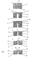
- FIG. 1 shows schematically the course of a preferred variant of the invention Method of making a preferred embodiment the device according to the invention.
- Fig. 2 shows the Process flow of a further variant of the invention Process.
- Fig. 1a shows schematically in section a part of a carrier or a substrate 2.
- the substrate 2 is essentially disc - shaped with two opposite, in essentially parallel surfaces 4, 6 educated.
- the substrate 2 preferably consists of Silicon, but can also be made of other materials, especially semiconductor materials are manufactured.
- a blind hole 8 is formed in the substrate 2.
- the blind hole 8 can, for example, by a method according to WO 99/58746 are trained.
- the etching process which too is also referred to as electrochemical pore etching detailed in EP 0 296 348 A, EP 0 645 621 A, WO 99/25026, EP 0 553 465 A and DE 198 20 756 are described. To this Publications are in full regarding the etching process Scope referred, so that their disclosure content as Part of the overall disclosure of the present application understand is.
- the blind hole extends from the Surface 6 is substantially normal to this in the direction of Surface 4.
- the blind hole 8 has a bottom 10, which in the interior of the substrate 2 from the surface 4th is spaced.
- the blind hole narrows towards the bottom 10 8.
- the blind hole 8 and in particular towards the bottom 10 narrowing area has essentially the shape of a pipette tip to be generated.
- the shape of the Blind hole 8 can thus be the shape of the one to be generated Pipette tip can be set.
- the electrochemical Pore etching process allows pores or blind holes with extremely large aspect ratio (ratio Blind hole diameter to depth). For example Aspect ratios of 1: 100 and more in regular Arrangements can be realized in silicon.
- the diameter of the Blind holes are preferably in the range from 0.5 to 20 ⁇ m, in particular 1 to 2 ⁇ m, and the distance (pitch) between the longitudinal central axes of the blind holes is preferred 10 ⁇ m to a few 100 ⁇ m.
- the depth of the blind holes can be in Range from about 100 to 5000 ⁇ m, which is typical Semiconductor wafer thicknesses included.
- the substrate 2 is provided with a modified surface layer 12.
- the modified surface layer 12 is formed both on the inner walls of the blind hole 8 and on the surfaces 4 and 6.
- the formation in the blind hole 8 is essential; a change in the surface layers on the surfaces 4 and 6 is not absolutely necessary, but is advantageous in terms of process technology.
- the surface layer 12 is formed in two layers, ie it consists of two layers lying one above the other. Alternatively, however, a single-layer training or training with more than two layers is also conceivable.
- the modified surface layer 12 is preferably formed by oxidation or nitriding, so that a layer of SiO 2 or Si 3 N 4 is formed.
- the surface layer 12 consists of a material which has the material properties desired for a pipette, and is advantageously formed from a material similar to the glass of a known patch pipette. Because the surface layer 12 is formed on the entire surface of the substrate 2, ie the surfaces 4, 6 and the inner walls of the blind hole 8, the coating or surface modification can be carried out very easily, since the entire substrate is oxidized and nitrided in a corresponding atmosphere or can be coated.
- Fig. 1d shows the next step in the process Surface layer 12 and part of the substrate 2 on the Surface 4 of the substrate 2 are removed. Doing so the substrate removed so far that the bottom 10 of the Blind hole 8 is opened.
- the substrate 2 and the surface layer 12 just removed so far that a Forms opening 14 with the desired size.
- the diameter of the opening 14 is 1 to 2 ⁇ m.
- the Removal is preferably carried out by chemical mechanical Polishing (CMP (chemical mechanical polishing)), however, can also be carried out by another suitable removal process. It is important that the removal is very precise to set the desired size of the opening 14 exactly can.
- CMP chemical mechanical polishing
- the next process step is shown in Fig. 1e.
- this process step finds a selective removal of the Substrate 2 instead. This is preferably done by etching, using an etchant which is only the substrate 2, but does not remove the surface layer 12 used.
- an etchant which is only the substrate 2, but does not remove the surface layer 12 used.
- This edge 16 from the surface layer 12 stands in front of the surface 4 of the substrate 2 and forms a pipette tip. In this pipette tip or this edge 16 is the opening 14 as a pipette opening educated.
- the fact that the surface layer 12 on the Surface 6 of the substrate 2 is formed, the Surface 6 not removed during selective removal.
- the etching process can be influenced how much of the Substrate 2 is removed. This allows the height to the edge or the pipette tip 16 from the surface 4 protrudes, can be set precisely.
- the removal of the substrate 2 on the surface 4 takes place at least in the area the blind hole or hole 8 to a protruding edge 16, which defines a pipette tip.
- a pipette tip 16 which is such can be designed to be essentially one corresponds to conventional patch pipette or a pressure channel for reproducible dispensing of the smallest Represents amounts of liquid on a surface.
- the arrangement according to the invention has the advantage that the Pipette tip 16 held and fixed in the substrate 2 is. In the way described can be very easily a large number of pipette tips 16 in the substrate 2 train at the same time. These pipette tips 16 are preferably in a predetermined grid or matrix arranged.
- Hole 8 which has arisen from blind hole 8, is on completely lined on the inside with the material, which forms the pipette tip 16. That way the entire end region of a patch pipette in the substrate 2 to provide.
- the Pipette in the substrate 2 also has a stray capacitance in the Area of the pipette wall, i.e. in this case the Surface layer 12, minimized.
- the surface layer 12 is formed in two layers. This causes the pipette tip 16 to have a different material on the outside than on the inside, ie inside the hole 8.
- the surface layer 12 can also be formed in one or more layers. Furthermore, it is not absolutely necessary to form the surface layer 12 on the entire inner surface of the hole 8 and on the surface 6. For example, only that part of the hole 8 which faces the edge 16 could be provided with the surface layer 12.
- the surface layer preferably consists of SiO 2 , since silicon oxide or silicon dioxide is very similar to the quartz glass used in conventional patch pipettes.
- Fig. 1b is also a through hole similar to that in Fig. 1d shown hole are formed. Furthermore, possibly without the surface layer 12 on the surface 4 become.
- the hole is the same as a through hole is trained on the first removal process possibly be dispensed with and the step of selective etching.
- that can Process combined with an upstream KOH etching process the lower, i.e. the edge 16 opposite Opening of the hole widens to the access resistance of the to reduce the resulting pipettes.
- Blind hole 8 is formed in a bubble shape in the substrate 2. Consequently the blind hole 8 has a starting from the surface 6 initially relatively small diameter, for example in the range from 0.5 ⁇ m to a few ⁇ m.
- a bubble-shaped area 22 on this Area 20 of the blind hole 8 close to the surface closes in Normal direction of the surface 6 is a bubble-shaped area 22 on, which has a larger inner diameter.
- the inner diameter of the bubble Range 22 be a few microns to 100 microns.
- the step of removing the substrate 2 starting from the Surface 4 is controlled in such a way that substrate 2 only up to the bubble-shaped area 22 of the blind hole 8 is removed. Since the inner walls of the blind hole 8 in one of the surface 6 of the bubble-shaped region 22 widening facing section results in a Pipette opening 14, the opening diameter of the distal end of the edge 16 enlarged. As in Fig. 2d) shown, pipette tips 16 can be made in this way with cup-shaped (Fig. 2 I) or tricher-shaped geometry
- the devices according to the invention are also suitable for the supply of synthetic materials and light for one localized, light-controlled synthesis of molecules.
- the pipettes of the devices according to the invention can be used as an optical fiber for selective, local Illumination of a substrate can be used.
- the individual Pipettes are optically isolated from each other and can be separated and used independently to transmit light become.
- the local lighting thus possible allows the light-induced chemical synthesis spatially limited perform.
- the possibility according to the invention Apply liquids locally and selectively at the same location Being able to illuminate thus opens up the material and time-saving locally isolated, light-driven chemical Synthesis of molecules.
- printable substrates for the invention 'Printhead' are suitable for all types of porous substrates, in particular porous silicon, aluminum oxide, silicates and porous organic materials such as nitrocellulose.
- porous substrates in particular porous silicon, aluminum oxide, silicates and porous organic materials such as nitrocellulose.
- pipette or pore size With decreasing pipette or pore size increase Capillary forces on liquids in contact with a porous Surface. Dispensing the volume of liquid from the Print head is created by the capillary action of the substrate facilitated.
Landscapes
- Engineering & Computer Science (AREA)
- Manufacturing & Machinery (AREA)
- Chemical & Material Sciences (AREA)
- Clinical Laboratory Science (AREA)
- Microelectronics & Electronic Packaging (AREA)
- Health & Medical Sciences (AREA)
- Analytical Chemistry (AREA)
- Chemical Kinetics & Catalysis (AREA)
- Apparatus Associated With Microorganisms And Enzymes (AREA)
- Devices For Use In Laboratory Experiments (AREA)
- Sampling And Sample Adjustment (AREA)
- Automatic Analysis And Handling Materials Therefor (AREA)
- Physical Or Chemical Processes And Apparatus (AREA)
Description
- 2
- Substrat
- 4, 6
- Oberflächen
- 8
- Sackloch, Loch
- 10
- Boden
- 12
- Oberflächenschicht
- 14
- Öffnung
- 16
- Rand, Pipettenspitze
- 18
- Kante
- 20
- oberflächennaher Bereich des Sacklochs 8
- 22
- blasenförmiger Bereich des Sacklochs 8
Claims (23)
- Vorrichtung; bei welcher in einem Substrat (2) zumindest eine Pipette in Form eines Durchgangsloches (8) mit einem vorbestimmten Durchmesser ausgebildet ist, wobei ein Rand (16) des Durchgangsloches (8) um ein vorbestimmtes Maß von einer benachbarten Oberfläche (4) des Substrats (2) vorsteht.
- Vorrichtung nach Anspruch 1, bei welcher zumindest der Rand (16) aus zumindest einem anderen Material als das Substrat (2) besteht und vorzugsweise SiO2 oder Si3N4 umfaßt.
- Vorrichtung nach Anspruch 1 oder 2, bei welcher eine Innenwandung des Durchgangsloches (8) zumindest teilweise aus einem anderen Material als das Substrat (2) besteht und vorzugsweise SiO2 oder Si3N4 umfaßt.
- Vorrichtung nach einem der vorangehenden Ansprüche, bei welcher die Innenseite des Randes (16) und vorzugsweise die Innenwandung des Durchgangsloches (8) aus einem anderen Material als die Außenseite des Randes (16) besteht.
- Vorrichtung nach einem der vorangehenden Ansprüche bei welcher an dem Rand und/oder an der Innenwandung des Durchgangsloches zumindest eine Schicht aus einem elektrisch leitfähigen Material ausgebildet ist.
- Vorrichtung nach einem der vorangehenden Ansprüche, bei welcher ein distales Ende (18) des Randes (16) gerundet ausgebildet ist.
- Vorrichtung nach einem der vorangehenden Ansprüche, bei welcher sich das Durchgangsloch (8) zu einem distalen Ende (18) des Randes (16) hin verengt oder aufweitet.
- Vorrichtung nach einem der vorangehenden Ansprüche, bei welcher das Substrat (2) aus Silizium besteht.
- Vorrichtung nach einem der vorangehenden Ansprüche, bei welcher in dem Substrat (2) mehrere Pipetten ausgebildet sind, welche vorzugsweise rasterartig in dem Substrat (2) angeordnet sind.
- Verfahren zum Ausbilden zumindest einer Pipette in einem Substrat (2) mit folgenden Schritten:wobei das Loch (8) in einem geeigneten Verfahrensschritt als Durchgangsloch ausgebildet wird.Ausbilden zumindest eines Loches (8),Ausbilden zumindest einer veränderten Oberflächenschicht (12) auf zumindest den Innenflächen des Loches (8),selektives Abtragen des Substrates (2), wobei die veränderte Oberflächenschicht (12) im wesentlichen nicht angegriffen wird, so daß diese über eine Oberfläche (4) des Substrats vorsteht und einen vorstehenden Rand (16) bildet,
- Verfahren nach Anspruch 10, bei welchem das Loch (8) zu der Seite hin, an welcher der Rand (16) ausgebildet wird, sich verjüngend ausgebildet wird.
- Verfahren nach Anspruch 10 oder 11, bei welchem das Loch (8) zunächst als Sackloch ausgebildet wird.
- Verfahren nach Anspruch 12, bei welchem nach Ausbilden des Sackloches (8) die einer Öffnung des Sackloches (8) entgegengesetzten Seite (4) des Substrats (2) bis zum Boden (10) des Sackloches (8) abgetragen wird, so daß das Sackloch (8) geöffnet wird, um ein Durchgangsloch (8) zu bilden.
- Verfahren nach Anspruch 12 oder 13, bei welchem das Sackloch (8) zu seinem Boden (10) hin verjüngend ausgebildet wird.
- Verfahren nach einem der Ansprüche 12 bis 14, bei welchem das Sackloch (8) durch Ätzen ausgebildet wird.
- Verfahren nach einem der Ansprüche 13 bis 15, bei welchem das Abtragen der der Öffnung des Sacklochs (8) entgegengesetzten Seite (4) des Substrats (2) durch chemisches und/oder mechanisches Abtragen erfolgt.
- Verfahren nach einem der Ansprüche 10 bis 16, bei welchem nach dem selektiven Abtragen die Kanten (18) des vorstehenden Randes (16) gerundet werden.
- Verfahren nach einem der Ansprüche 10 bis 17, bei welchem die veränderte Oberflächenschicht (12) zusätzlich auf einer Oberfläche (4; 6) des Substrats (2) ausgebildet wird.
- Verfahren nach einem der Ansprüche 10 bis 18, bei welchem die veränderte Oberflächenschicht (12) auf der gesamten Oberfläche (4, 6) des Substrats (2) ausgebildet wird und auf Seite (4) des Substrats (2), an welcher der Rand (16) ausgebildet wird, vor dem selektiven Abtragen vorzugsweise chemisch und/oder mechanisch abgetragen wird.
- Verfahren nach einem der Ansprüche 10 bis 19, bei welchem das selektive Abtragen des Substrats (2) durch Ätzen erfolgt,
wobei ein Ätzmittel verwendet wird, welches die veränderte Oberflächenschicht (12) im wesentlichen nicht angreift. - Verfahren nach einem der Ansprüche 10 bis 20, bei welchem das Substrat (2) aus einem Material besteht, welches ein Halbleitermaterial und insbesondere Silizium umfaßt.
- Verfahren nach einem der Ansprüche 10 bis 21, bei welchem zumindest die veränderte Oberflächenschicht (12) durch Beschichten und/oder Modifizieren der Oberfläche des Substrats (2), insbesondere Oxidieren oder Nitrieren
- Verfahren nach einem der Ansprüche 10 bis 22, bei welchem die veränderte Oberflächenschicht (12) zumindest im Bereich des Loches (8) zumindest abschnittweise mehrere Schichten aus vorzugsweise verschiedenen Materialien aufweist.
Applications Claiming Priority (3)
| Application Number | Priority Date | Filing Date | Title |
|---|---|---|---|
| DE10130218A DE10130218A1 (de) | 2001-06-22 | 2001-06-22 | Vorrichtung für ein Patch-Clamping von Vesikeln und Verfahren zu deren Herstellung |
| DE10130218 | 2001-06-22 | ||
| PCT/EP2002/006855 WO2003000421A1 (de) | 2001-06-22 | 2002-06-20 | Pipettenvorrichtung und verfahren zu deren herstellung |
Publications (2)
| Publication Number | Publication Date |
|---|---|
| EP1399262A1 EP1399262A1 (de) | 2004-03-24 |
| EP1399262B1 true EP1399262B1 (de) | 2004-10-13 |
Family
ID=7689126
Family Applications (1)
| Application Number | Title | Priority Date | Filing Date |
|---|---|---|---|
| EP02754726A Expired - Lifetime EP1399262B1 (de) | 2001-06-22 | 2002-06-20 | Pipettenvorrichtung und verfahren zu deren herstellung |
Country Status (6)
| Country | Link |
|---|---|
| US (1) | US20040156754A1 (de) |
| EP (1) | EP1399262B1 (de) |
| JP (1) | JP2005500519A (de) |
| AT (1) | ATE279259T1 (de) |
| DE (2) | DE10130218A1 (de) |
| WO (1) | WO2003000421A1 (de) |
Families Citing this family (5)
| Publication number | Priority date | Publication date | Assignee | Title |
|---|---|---|---|---|
| KR100666825B1 (ko) * | 2005-03-26 | 2007-01-11 | 한국표준과학연구원 | 전기전도성 관을 이용한 전기삼투압류 구동 극미세 피펫장치 |
| WO2007108773A1 (en) * | 2006-03-23 | 2007-09-27 | Agengy For Science, Technology And Research | Device for analyzing the status of a particle |
| WO2009023448A1 (en) | 2007-08-13 | 2009-02-19 | Polyone Corporation | Electrically conductive polyolefin blends |
| DE102012002459B4 (de) * | 2012-02-08 | 2015-06-25 | Universität Rostock | Elektrophysiologische Messanordnung und elektrophysiologisches Messverfahren |
| CN115851417A (zh) * | 2023-02-16 | 2023-03-28 | 季华实验室 | Pcr管、pcr芯片、扩增加热装置和pcr操作方法 |
Family Cites Families (7)
| Publication number | Priority date | Publication date | Assignee | Title |
|---|---|---|---|---|
| JP3640089B2 (ja) * | 1995-03-17 | 2005-04-20 | リコープリンティングシステムズ株式会社 | ピペットの製造方法 |
| KR0170190B1 (ko) * | 1995-12-06 | 1999-03-30 | 정선종 | 씨디엠에이 이동통신 시스템에서 트래픽 부하 제어방법 |
| DE19744649C2 (de) * | 1997-10-09 | 2003-03-27 | Fraunhofer Ges Forschung | Verfahren zur Messung bioelektrischer Signale von Zellen nach der Patch-Clamp-Methode sowie Verwendung einer Vorrichtung hierzu |
| DE19827957C2 (de) * | 1998-05-27 | 2000-06-29 | Micronas Intermetall Gmbh | Verfahren und Vorrichtung zur Messung einer Zustandsgröße |
| ATE513209T1 (de) * | 1998-12-05 | 2011-07-15 | Xention Ltd | Grenzflächen-patch-clamp-verfahren und -gerät |
| DE19936302A1 (de) * | 1999-08-02 | 2001-02-15 | Niels Fertig | Vorrichtungen und Verfahren zur Untersuchung von Ionenkanälen in Membranen |
| DE29919506U1 (de) * | 1999-11-05 | 2000-02-24 | CREAVIS Gesellschaft für Technologie und Innovation mbH, 45772 Marl | Mikrostruktuierte Pipetten als Dosiersysteme |
-
2001
- 2001-06-22 DE DE10130218A patent/DE10130218A1/de not_active Withdrawn
-
2002
- 2002-06-20 AT AT02754726T patent/ATE279259T1/de not_active IP Right Cessation
- 2002-06-20 JP JP2003507054A patent/JP2005500519A/ja not_active Abandoned
- 2002-06-20 EP EP02754726A patent/EP1399262B1/de not_active Expired - Lifetime
- 2002-06-20 DE DE2002501320 patent/DE50201320D1/de not_active Expired - Fee Related
- 2002-06-20 WO PCT/EP2002/006855 patent/WO2003000421A1/de not_active Ceased
-
2003
- 2003-12-22 US US10/745,473 patent/US20040156754A1/en not_active Abandoned
Also Published As
| Publication number | Publication date |
|---|---|
| US20040156754A1 (en) | 2004-08-12 |
| WO2003000421A1 (de) | 2003-01-03 |
| ATE279259T1 (de) | 2004-10-15 |
| EP1399262A1 (de) | 2004-03-24 |
| DE50201320D1 (de) | 2004-11-18 |
| JP2005500519A (ja) | 2005-01-06 |
| DE10130218A1 (de) | 2003-01-09 |
Similar Documents
| Publication | Publication Date | Title |
|---|---|---|
| EP1218736B1 (de) | Vorrichtung zum messen an in einer flüssigen umgebung befindlichen zellen | |
| DE69730667T2 (de) | Verfahren zur Herstellung eines Durchgangslochs, Gebrauch dieses Verfahrens zur Herstellung eines Slikonsubstrates mit einem solchen Durchgangsloch oder eine Vorrichtung mit diesem Substrat, Verfahren zur Herstellung eines Tintenstrahl-Druckkopfes und Gebrauch dieses Verfahrens zur Herstellung eines Tintenstrahldruckkopfes | |
| DE60205413T2 (de) | Herstellungsverfahren | |
| EP1349916A2 (de) | Vorrichtung und verfahren zur untersuchung von ionenkanälen in membranen | |
| DE19936302A1 (de) | Vorrichtungen und Verfahren zur Untersuchung von Ionenkanälen in Membranen | |
| DE10332725A1 (de) | Verfahren zur selbstjustierenden Verkleinerung von Strukturen | |
| DE602004013195T2 (de) | Planare elektrosprühquellen auf grundlage einer kalligraphiefeder und herstellung davon | |
| DE60307095T2 (de) | Vorrichtung zur aktiv gesteuerten und lokalisierten ablagerung mindestens einer biologischen lösung | |
| DE69529642T2 (de) | Vorrichtung zur Emission von Elektronen | |
| EP1399262B1 (de) | Pipettenvorrichtung und verfahren zu deren herstellung | |
| DE19705910C1 (de) | Mikrokammerarray mit hoher Kammerdichte | |
| EP1381467A2 (de) | Verfahren und vorrichtung zur manipulation kleiner flüssigkeitsmengen auf oberflächen | |
| EP1546029A1 (de) | Verfahren zur herstellung einer mikromechanischen vorrichtung, insbesondere einer mikromechanischen schwingspiegelvorrichtung | |
| DE102008005350A1 (de) | Mikrofluidische Vorrichtungen mit Nanokanälen | |
| DE102018215255A1 (de) | Dreidimensionaler nanostrukturkörper und verfahren zum herstellen eines dreidimensionalen nanostrukturkörpers | |
| EP2663860B1 (de) | Mikrostrukturvorrichtung zur messung an molekularen membranen und ein verfahren zur herstellung dieser mikrostrukturvorrichtung | |
| EP1527012A2 (de) | Verfahren und herstellung wenigstens einer kleinen öffnung in einer schicht auf einem substrat und damit hergestellte bauelemente | |
| EP1042794A1 (de) | Verfahren zur herstellung einer porösen schicht mit hilfe eines elektrochemischen ätzprozesses | |
| DE19628052C1 (de) | Sensor- und/oder Trennelement sowie Verfahren zu dessen Herstellung und Anwendung desselben | |
| EP3736050B1 (de) | Vorrichtung und verfahren zum aufbringen flüssiger medien auf eine substratoberfläche | |
| DE102006024286B4 (de) | Mikrofluidische Vorrichtung, insbesondere zur Dosierung einer Flüssigkeit oder zur dosierten Abgabe einer Flüssigkeit, und Verfahren zur Herstellung einer mikrofluidischen Vorrichtung | |
| DE19638501A1 (de) | Verfahren zur Herstellung einer Kapillare | |
| DE19509903A1 (de) | Verfahren zur Herstellung einer Abtastvorrichtung zur kombinierten Untersuchung von verschiedenen Oberflächeneigenschaften mit Auflösung im Nanometerbereich | |
| DE10236149A1 (de) | Verfahren zur Herstellung einer eine schmale Schneide oder Spitze aufweisenden Struktur und mit einer solchen Struktur versehener Biegebalken | |
| DE69926948T2 (de) | Tintenstrahlaufzeichnungskopf und Tintenstrahlaufzeichnungsvorrichtung |
Legal Events
| Date | Code | Title | Description |
|---|---|---|---|
| PUAI | Public reference made under article 153(3) epc to a published international application that has entered the european phase |
Free format text: ORIGINAL CODE: 0009012 |
|
| 17P | Request for examination filed |
Effective date: 20031218 |
|
| AK | Designated contracting states |
Kind code of ref document: A1 Designated state(s): AT BE CH CY DE DK ES FI FR GB GR IE IT LI LU MC NL PT SE TR |
|
| GRAP | Despatch of communication of intention to grant a patent |
Free format text: ORIGINAL CODE: EPIDOSNIGR1 |
|
| GRAS | Grant fee paid |
Free format text: ORIGINAL CODE: EPIDOSNIGR3 |
|
| GRAA | (expected) grant |
Free format text: ORIGINAL CODE: 0009210 |
|
| AK | Designated contracting states |
Kind code of ref document: B1 Designated state(s): AT BE CH CY DE DK ES FI FR GB GR IE IT LI LU MC NL PT SE TR |
|
| PG25 | Lapsed in a contracting state [announced via postgrant information from national office to epo] |
Ref country code: TR Free format text: LAPSE BECAUSE OF FAILURE TO SUBMIT A TRANSLATION OF THE DESCRIPTION OR TO PAY THE FEE WITHIN THE PRESCRIBED TIME-LIMIT Effective date: 20041013 Ref country code: NL Free format text: LAPSE BECAUSE OF FAILURE TO SUBMIT A TRANSLATION OF THE DESCRIPTION OR TO PAY THE FEE WITHIN THE PRESCRIBED TIME-LIMIT Effective date: 20041013 Ref country code: IT Free format text: LAPSE BECAUSE OF FAILURE TO SUBMIT A TRANSLATION OF THE DESCRIPTION OR TO PAY THE FEE WITHIN THE PRESCRIBED TIME-LIMIT;WARNING: LAPSES OF ITALIAN PATENTS WITH EFFECTIVE DATE BEFORE 2007 MAY HAVE OCCURRED AT ANY TIME BEFORE 2007. THE CORRECT EFFECTIVE DATE MAY BE DIFFERENT FROM THE ONE RECORDED. Effective date: 20041013 Ref country code: IE Free format text: LAPSE BECAUSE OF FAILURE TO SUBMIT A TRANSLATION OF THE DESCRIPTION OR TO PAY THE FEE WITHIN THE PRESCRIBED TIME-LIMIT Effective date: 20041013 Ref country code: FI Free format text: LAPSE BECAUSE OF FAILURE TO SUBMIT A TRANSLATION OF THE DESCRIPTION OR TO PAY THE FEE WITHIN THE PRESCRIBED TIME-LIMIT Effective date: 20041013 Ref country code: ES Free format text: LAPSE BECAUSE OF FAILURE TO SUBMIT A TRANSLATION OF THE DESCRIPTION OR TO PAY THE FEE WITHIN THE PRESCRIBED TIME-LIMIT Effective date: 20041013 |
|
| REG | Reference to a national code |
Ref country code: GB Ref legal event code: FG4D Free format text: NOT ENGLISH |
|
| REG | Reference to a national code |
Ref country code: CH Ref legal event code: EP |
|
| REG | Reference to a national code |
Ref country code: IE Ref legal event code: FG4D Free format text: GERMAN |
|
| REF | Corresponds to: |
Ref document number: 50201320 Country of ref document: DE Date of ref document: 20041118 Kind code of ref document: P |
|
| PG25 | Lapsed in a contracting state [announced via postgrant information from national office to epo] |
Ref country code: SE Free format text: LAPSE BECAUSE OF FAILURE TO SUBMIT A TRANSLATION OF THE DESCRIPTION OR TO PAY THE FEE WITHIN THE PRESCRIBED TIME-LIMIT Effective date: 20050113 Ref country code: GR Free format text: LAPSE BECAUSE OF FAILURE TO SUBMIT A TRANSLATION OF THE DESCRIPTION OR TO PAY THE FEE WITHIN THE PRESCRIBED TIME-LIMIT Effective date: 20050113 Ref country code: DK Free format text: LAPSE BECAUSE OF FAILURE TO SUBMIT A TRANSLATION OF THE DESCRIPTION OR TO PAY THE FEE WITHIN THE PRESCRIBED TIME-LIMIT Effective date: 20050113 |
|
| GBT | Gb: translation of ep patent filed (gb section 77(6)(a)/1977) |
Effective date: 20050203 |
|
| NLV1 | Nl: lapsed or annulled due to failure to fulfill the requirements of art. 29p and 29m of the patents act | ||
| REG | Reference to a national code |
Ref country code: IE Ref legal event code: FD4D |
|
| PGFP | Annual fee paid to national office [announced via postgrant information from national office to epo] |
Ref country code: FR Payment date: 20050610 Year of fee payment: 4 |
|
| PG25 | Lapsed in a contracting state [announced via postgrant information from national office to epo] |
Ref country code: LU Free format text: LAPSE BECAUSE OF NON-PAYMENT OF DUE FEES Effective date: 20050620 Ref country code: CY Free format text: LAPSE BECAUSE OF FAILURE TO SUBMIT A TRANSLATION OF THE DESCRIPTION OR TO PAY THE FEE WITHIN THE PRESCRIBED TIME-LIMIT Effective date: 20050620 Ref country code: AT Free format text: LAPSE BECAUSE OF NON-PAYMENT OF DUE FEES Effective date: 20050620 |
|
| PG25 | Lapsed in a contracting state [announced via postgrant information from national office to epo] |
Ref country code: MC Free format text: LAPSE BECAUSE OF NON-PAYMENT OF DUE FEES Effective date: 20050630 Ref country code: BE Free format text: LAPSE BECAUSE OF NON-PAYMENT OF DUE FEES Effective date: 20050630 |
|
| PLBE | No opposition filed within time limit |
Free format text: ORIGINAL CODE: 0009261 |
|
| STAA | Information on the status of an ep patent application or granted ep patent |
Free format text: STATUS: NO OPPOSITION FILED WITHIN TIME LIMIT |
|
| ET | Fr: translation filed | ||
| 26N | No opposition filed |
Effective date: 20050714 |
|
| PG25 | Lapsed in a contracting state [announced via postgrant information from national office to epo] |
Ref country code: DE Free format text: LAPSE BECAUSE OF NON-PAYMENT OF DUE FEES Effective date: 20060103 |
|
| PG25 | Lapsed in a contracting state [announced via postgrant information from national office to epo] |
Ref country code: GB Free format text: LAPSE BECAUSE OF NON-PAYMENT OF DUE FEES Effective date: 20060620 |
|
| PG25 | Lapsed in a contracting state [announced via postgrant information from national office to epo] |
Ref country code: LI Free format text: LAPSE BECAUSE OF NON-PAYMENT OF DUE FEES Effective date: 20060630 Ref country code: CH Free format text: LAPSE BECAUSE OF NON-PAYMENT OF DUE FEES Effective date: 20060630 |
|
| REG | Reference to a national code |
Ref country code: CH Ref legal event code: PL |
|
| GBPC | Gb: european patent ceased through non-payment of renewal fee |
Effective date: 20060620 |
|
| REG | Reference to a national code |
Ref country code: FR Ref legal event code: ST Effective date: 20070228 |
|
| BERE | Be: lapsed |
Owner name: *INFINEON TECHNOLOGIES A.G. Effective date: 20050630 |
|
| PG25 | Lapsed in a contracting state [announced via postgrant information from national office to epo] |
Ref country code: PT Free format text: LAPSE BECAUSE OF NON-PAYMENT OF DUE FEES Effective date: 20050313 |
|
| PG25 | Lapsed in a contracting state [announced via postgrant information from national office to epo] |
Ref country code: FR Free format text: LAPSE BECAUSE OF NON-PAYMENT OF DUE FEES Effective date: 20060630 |