EP1400014B1 - Leistungsverstärker (pa) mit verbesserter leistungsregelung - Google Patents
Leistungsverstärker (pa) mit verbesserter leistungsregelung Download PDFInfo
- Publication number
- EP1400014B1 EP1400014B1 EP02764570A EP02764570A EP1400014B1 EP 1400014 B1 EP1400014 B1 EP 1400014B1 EP 02764570 A EP02764570 A EP 02764570A EP 02764570 A EP02764570 A EP 02764570A EP 1400014 B1 EP1400014 B1 EP 1400014B1
- Authority
- EP
- European Patent Office
- Prior art keywords
- power amplifier
- output
- power
- circuit
- load
- Prior art date
- Legal status (The legal status is an assumption and is not a legal conclusion. Google has not performed a legal analysis and makes no representation as to the accuracy of the status listed.)
- Expired - Lifetime
Links
Images



Classifications
-
- H—ELECTRICITY
- H03—ELECTRONIC CIRCUITRY
- H03G—CONTROL OF AMPLIFICATION
- H03G3/00—Gain control in amplifiers or frequency changers
- H03G3/20—Automatic control
- H03G3/30—Automatic control in amplifiers having semiconductor devices
- H03G3/3036—Automatic control in amplifiers having semiconductor devices in high-frequency amplifiers or in frequency-changers
- H03G3/3042—Automatic control in amplifiers having semiconductor devices in high-frequency amplifiers or in frequency-changers in modulators, frequency-changers, transmitters or power amplifiers
Definitions
- the present invention is generally related to power amplifiers, and, more specifically, to a system and method for regulating the power produced by a power amplifier.
- the output power of a transmitter within a communication device has to be well controlled due to the specifications of the communication system.
- the output power of the transmitter is generated by a power amplifier, which is controlled by a control circuit.
- the load impedance (R) changes, the output power (P) will change (assuming I is kept constant).
- Changes to the load impedance are commonly caused by environmental factors. For example, if the load is an antenna of a transmitter for transmitting signals, the load impedance is dependent upon the environment surrounding the antenna. As an example, if a mobile phone is held in the hand, the impedance "felt" by the power amplifier may be different from the impedance felt by the power amplifier when the mobile phone is sitting on a table or in a car. Because the output power must be well controlled, it is desired to keep the output power constant, regardless of changes in the load impedance.
- US 6 008 698 discloses an amplifier with dynamically adaptable supply current comprising an adaptable DC power consumption circuit, wherein the current supplied to an RF amplifier is dynamically varied from a desired level.
- a feedback control loop is formed between the power terminal and the control terminal of the RF amplifier.
- a controller influences the feedback control loop to properly set the supply current at the desired minimum level necessary to maintain linear operation of the RF amplifier.
- the output of the RF amplifier influences the feedback control loop to dynamically vary the supply current from the desired level.
- FIG. 1 illustrates a conventional circuit for controlling the output power of a power amplifier 102.
- the current (I 1 ) flowing into power amplifier 102 is measured.
- I 1 is a good measure of the power produced by power amplifier 102.
- This current is measured by measuring the voltage at node N1.
- This voltage is referred to as Vsense.
- L1 is an RF-choke inductor.
- a control circuit 108 compares Vsense to a reference voltage (Vref).
- Control circuit 108 controls the output power of power amplifier 102 based on the result of the comparison between Vsense and Vref. In this manner, the circuit shown in FIG. 1 may control the output power of power amplifier 102 based on the measured current (I 1 ) flowing into the power amplifier 102.
- the circuit shown in FIG. 1 suffers from several disadvantages, one of which is that it has difficulty achieving high dynamics.
- Embodiments of the present invention which is defined in the claims provide a system and method for improving the power regulation of a power amplifier circuit. More specifically, the present invention improves control of output power in the situations where there is an impedance mismatch at the output.
- a method of the present invention includes the steps of (1) comparing a measured signal to a reference signal, wherein the measured signal represents the sum of the amplitude of the output voltage of the power amplifier and a current flowing into the power amplifier from a power supply connected to the power amplifier and (2) controlling the power amplifier based on the result of the comparison between the measured signal and the reference signal.
- a circuit of the present invention includes a current detector for measuring the current flowing into the power amplifier from a power supply, an amplitude detector that measures the amplitude of the output voltage of the power amplifier, an adder for summing the output of the current detector and the amplitude detector, and a control circuit connected to a biasing pin of the power amplifier that compares the output of the adder to a reference signal and controls the power amplifier based on the result of the comparison between the reference signal and the output of the adder.
- the output of the adder changes as the impedance of the load on the power amplifier changes.
- the output of the control circuit will change when the output of the adder changes, the output of the control circuit changes when the impedance of the load changes.
- the output of the control circuit is connected to the biasing input of the power amplifier, the output of the control circuit controls the current delivered by the power amplifier to the load, and, hence, controls the power delivered to the load.
- the control circuit increases or decreases the current delivered to the load, depending on the change in the impedance of the load. In this manner, the control circuit regulates the power delivered by the power amplifier to the load and can keep the output power constant, regardless of changes in the load.
- FIG. 6 is a flow chart illustrating a process 600, according to one embodiment of the invention, for controlling the output power of a power amplifier circuit.
- Process 600 begins with step 602, wherein a measurement corresponding to a current flowing into the power amplifier from a power source is produced.
- step 604 a measurement corresponding to the amplitude of an output signal produced by the power amplifier is produced.
- step 606 the measurements from step 602 and 604 are added together.
- the resulting sum is compared to a reference.
- the power amplifier is controlled based on the result of the comparison. In this manner, the method of the present invention regulates the output power of a power amplifier circuit.
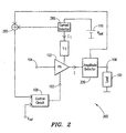
- FIG. 2 illustrates a high level circuit diagram that illustrates a power amplifier circuit 200 according to one embodiment.
- Power amplifier circuit 200 includes power amplifier 102 that functions to receive an input signal at its input 104 and to amplify the input signal to produce an output signal at its output 106.
- Circuit 200 also includes a control circuit 108 for controlling the output power of power amplifier 102. More specifically, control circuit 108 functions to keep the output power of power amplifier 102 constant, regardless of changes in the impedance of a load 105 connected to the output 106 of power amplifier 102. The output of control circuit 108 is connected to a biasing control pin 103 of power amplifier 102. Thus, the output of control circuit 108 affects the amount of current (I) provided to load 105.
- I current
- Circuit 200 also includes power source 110 (Vbat) that provides power to power amplifier 102, a current detector 280 for measuring the current flowing out of power source 110, an amplitude detector 220 for measuring the amplitude of the output signal of power amplifier 102, and an adder 285 for adding the outputs of current detector 280 and amplitude detector 220.
- the output of adder 285 is provided to an input of control circuit 108.
- control circuit 108 Provided to another input of control circuit 108 is the reference signal (Vref). Controller 108 controls power amplifier 102 based on the difference between the output of adder 285 and the reference signal.
- control circuit 108 is a comparator. That is, control circuit 108 compares the output of adder 285 to the reference signal and outputs a voltage that corresponds to the difference between the two inputs. The output of adder 285 changes when the real part of the impedance of load 105 changes. Thus, because the output of control circuit 108 will change when the output of adder 285 changes, the output of control circuit 108 changes when the impedance of load 105 changes. As discussed above, the output of control circuit 108 affects the current (I) delivered by power amplifier 102 to load 105. Consequently, when the impedance of load 105 changes, control circuit 108 increases or decreases the current delivered to load 105, depending on the impedance of load 105. In this manner, control circuit 108 regulates the power delivered by power amplifier 102 to load 105 and can keep the output power constant, regardless of changes in the load.
- I current
- FIG. 3 illustrates circuit 200 in greater detail according to one embodiment.
- current detector 280 is implemented with a resistor (R1)
- adder 285 is implemented with a resistor (R2)
- amplitude detector 220 is implemented with an envelope detector 320 and a voltage to current generator 322.
- Detector circuit 320 functions to output a voltage that corresponds to the amplitude of the output signal produced by power amplifier 102.
- Voltage to current generator 322 receives as input the output of detector circuit 320.
- the output of generator 322 is connected to adder 285.
- Generator 322 converts the voltage outputted by circuit 320 to a current I 2 . This current is drawn through resistors R1 and R2 (R2 is preferably greater than R1).
- FIG. 4 is a schematic of one embodiment of detector circuit 320.
- detector circuit 320 includes a diode 401 connected in series with a resistance (R3) connected in parallel with a capacitance (C1).
- the input to the detector circuit 320 is the output 106 of power amplifier 102.
- the output of detector circuit 320 is a voltage that corresponds to the amplitude of the output signal 106 of power amplifier 102.
- detector circuit 320 is also referred to as an amplitude detector or envelope detector.
- FIG. 4 is used merely for illustration and not limitation.
- FIG. 5 is a schematic of one embodiment of voltage to current generator 322.
- generator 322 includes a bi-polar junction transistor 502.
- the input of generator 322 is connected to the base 504 of transistor 502 through a resistance (R4).
- the base 504 is also connected to ground through a resistance (R5).
- the emitter 506 is connected to ground through a resistance (R6), and the collector 508 is the output terminal of generator 322.
- R4 resistance
- R5 resistance
- R6 resistance
- FIG. 5 is used merely for illustration and not limitation.
- the present invention improves control of the output power in the situations where there is an impedance mismatch at the output.
- amplitude detector circuit 220 together with the current sensing protects power amplifier 102 from over voltage peaks.
Landscapes
- Amplifiers (AREA)
Claims (10)
- Schaltung (200) zum Verstärken eines Eingangssignals, die folgendes aufweist:einen Leistungsverstärker (102), der das Eingangssignal empfängt und ein Ausgangssignal erzeugt;einen Amplitudendetektor (220), der mit einem Ausgang des Leistungsverstärkers gekoppelt ist, welcher Detektor einen Messwert erzeugt, der der Amplitude des Ausgangssignals entspricht;eine Energiequelle zum Liefern von Energie zum Leistungsverstärker;einen Stromdetektor (280), der einen zweiten Messwert erzeugt, der dem Strom entspricht, der von der Energiequelle in den Leistungsverstärker fließt;einen Addierer (285) zum Addieren des ersten Messwertes mit dem zweiten Messwert zum Erzeugen eines dritten Messwerts; undeine Steuerschaltung (108), die an einen Vorspannungspin des Leistungsverstärkers angeschlossen ist, zum Vergleichen des dritten Messwerts mit einer Referenz und zum Steuern der Ausgangsleistung des Leistungsverstärkers (102) basierend auf dem Vergleich.
- Schaltung nach Anspruch 1, wobei der Amplitudendetektor einen Hüllkurvendetektor (320) aufweist.
- Schaltung nach Anspruch 2, wobei der Hüllkurvendetektor eine Diode (401) und einen Widerstand (R3) aufweist, der parallel zu einem Kondensator (C1) geschaltet ist, wobei die Diode (401) in Reihe zu dem Widerstand (R3) und dem Kondensator (C1) geschaltet ist.
- Schaltung nach Anspruch 3, wobei der Amplitudendetektor weiterhin einen Spannung-zu-Strom-Generator (322) aufweist, der eine Ausgangsspannung vom Hüllkurvendetektor (320) empfängt und die Ausgangsspannung in einen Strom umwandelt.
- Schaltung nach Anspruch 3, wobei der Spannung-zu-Strom-Generator einen Transistor (102) aufweist.
- Schaltung nach Anspruch 1, wobei der Stromdetektor (280) einen ersten Widerstand (R1) aufweist und der Addierer (285) einen zweiten Widerstand (R2) aufweist, wobei der Widerstandswert des zweiten Widerstands (R2) größer als der Widerstandswert des ersten Widerstands (R1) ist.
- Funkkommunikationsvorrichtung mit einer Schaltung nach Anspruch 1.
- Verfahren, das die folgenden Schritte aufweist:Erzeugen (602) einer ersten Messung entsprechend dem Ausmaß an Strom, der von einer Energiequelle in einen Leistungsverstärker fließt;Erzeugen (604) einer zweiten Messung entsprechend der Amplitude eines durch den Leistungsverstärker erzeugten Ausgangssignals;Addieren (606) der ersten Messung zu der zweiten Messung, um eine Summe zu erzeugen;Vergleichen (608) der Summe mit einer Referenz;Steuern (610) des Leistungsverstärkers basierend auf einem Ergebnis des Vergleichs.
- Verfahren nach Anspruch 8, wobei der Schritt (610) zum Steuern des Leistungsverstärkers den Schritt zum Anlegen einer Spannung an einen Vorspannungspin (103) des Leistungsverstärkers (102) aufweist.
- Verfahren nach Anspruch 9, wobei die Größe der Spannung eine Funktion der Differenz zwischen der Summe und der Referenz ist.
Applications Claiming Priority (3)
| Application Number | Priority Date | Filing Date | Title |
|---|---|---|---|
| US09/874,130 US7062237B2 (en) | 2001-06-05 | 2001-06-05 | Power amplifier (PA) with improved power regulation |
| US874130 | 2001-06-05 | ||
| PCT/EP2002/005608 WO2002099967A1 (en) | 2001-06-05 | 2002-05-22 | Power amplifier (pa) with improved power regulation |
Publications (2)
| Publication Number | Publication Date |
|---|---|
| EP1400014A1 EP1400014A1 (de) | 2004-03-24 |
| EP1400014B1 true EP1400014B1 (de) | 2006-02-22 |
Family
ID=25363040
Family Applications (1)
| Application Number | Title | Priority Date | Filing Date |
|---|---|---|---|
| EP02764570A Expired - Lifetime EP1400014B1 (de) | 2001-06-05 | 2002-05-22 | Leistungsverstärker (pa) mit verbesserter leistungsregelung |
Country Status (5)
| Country | Link |
|---|---|
| US (1) | US7062237B2 (de) |
| EP (1) | EP1400014B1 (de) |
| AT (1) | ATE318464T1 (de) |
| DE (1) | DE60209363T2 (de) |
| WO (1) | WO2002099967A1 (de) |
Families Citing this family (25)
| Publication number | Priority date | Publication date | Assignee | Title |
|---|---|---|---|---|
| US6856199B2 (en) * | 2000-10-10 | 2005-02-15 | California Institute Of Technology | Reconfigurable distributed active transformers |
| AU2002224368A1 (en) | 2000-10-10 | 2002-04-22 | California Institute Of Technology | Distributed circular geometry power amplifier architecture |
| US20030119460A1 (en) * | 2001-12-26 | 2003-06-26 | Eliav Zipper | Transmitted power level indicator |
| TWI326967B (en) | 2002-03-11 | 2010-07-01 | California Inst Of Techn | Differential amplifier |
| US7355470B2 (en) | 2006-04-24 | 2008-04-08 | Parkervision, Inc. | Systems and methods of RF power transmission, modulation, and amplification, including embodiments for amplifier class transitioning |
| US7327803B2 (en) | 2004-10-22 | 2008-02-05 | Parkervision, Inc. | Systems and methods for vector power amplification |
| US7738849B2 (en) * | 2005-10-14 | 2010-06-15 | Avago Technologies Wireless Ip (Singapore) Pte. Ltd. | Output impedance insensitive power amplifier architecture |
| US7911272B2 (en) | 2007-06-19 | 2011-03-22 | Parkervision, Inc. | Systems and methods of RF power transmission, modulation, and amplification, including blended control embodiments |
| US20130078934A1 (en) | 2011-04-08 | 2013-03-28 | Gregory Rawlins | Systems and Methods of RF Power Transmission, Modulation, and Amplification |
| US8013675B2 (en) | 2007-06-19 | 2011-09-06 | Parkervision, Inc. | Combiner-less multiple input single output (MISO) amplification with blended control |
| US8031804B2 (en) | 2006-04-24 | 2011-10-04 | Parkervision, Inc. | Systems and methods of RF tower transmission, modulation, and amplification, including embodiments for compensating for waveform distortion |
| US7937106B2 (en) | 2006-04-24 | 2011-05-03 | ParkerVision, Inc, | Systems and methods of RF power transmission, modulation, and amplification, including architectural embodiments of same |
| US7486137B2 (en) * | 2006-09-08 | 2009-02-03 | Axiom Microdevices, Inc. | System and method for power amplifier output power control |
| WO2008144017A1 (en) | 2007-05-18 | 2008-11-27 | Parkervision, Inc. | Systems and methods of rf power transmission, modulation, and amplification |
| WO2009005768A1 (en) | 2007-06-28 | 2009-01-08 | Parkervision, Inc. | Systems and methods of rf power transmission, modulation, and amplification |
| US7710197B2 (en) * | 2007-07-11 | 2010-05-04 | Axiom Microdevices, Inc. | Low offset envelope detector and method of use |
| US7941110B2 (en) * | 2007-07-23 | 2011-05-10 | Freescale Semiconductor, Inc. | RF circuit with control unit to reduce signal power under appropriate conditions |
| US20100330938A1 (en) * | 2008-03-13 | 2010-12-30 | Freescale Semiconductor, Inc. | Power detector |
| WO2009145887A1 (en) | 2008-05-27 | 2009-12-03 | Parkervision, Inc. | Systems and methods of rf power transmission, modulation, and amplification |
| DE102009050491A1 (de) * | 2009-10-23 | 2011-04-28 | Rohde & Schwarz Gmbh & Co. Kg | Kompensationsschaltung zur Verbesserung der Pegelregelung integrierter Verstärkerbausteine |
| EP2715867A4 (de) | 2011-06-02 | 2014-12-17 | Parkervision Inc | Antennensteuerung |
| WO2015042142A1 (en) | 2013-09-17 | 2015-03-26 | Parkervision, Inc. | Method, apparatus and system for rendering an information bearing function of time |
| US20180145668A1 (en) * | 2016-11-22 | 2018-05-24 | Mosway Technologies Limited | Voltage clamping circuit |
| US10965255B1 (en) * | 2019-10-30 | 2021-03-30 | Psemi Corporation | Overvoltage protection for power amplifier with soft shutdown |
| US12525922B2 (en) | 2022-08-23 | 2026-01-13 | Psemi Corporation | Over temperature protection with soft shutdown for power amplifier |
Family Cites Families (6)
| Publication number | Priority date | Publication date | Assignee | Title |
|---|---|---|---|---|
| US3449680A (en) | 1966-03-29 | 1969-06-10 | Motorola Inc | Transistor protection circuit |
| US5285143A (en) * | 1991-08-06 | 1994-02-08 | International Business Machines Corporation | Measurement of load current in a multi-phase power amplifier |
| SE508506C2 (sv) * | 1997-02-25 | 1998-10-12 | Ericsson Telefon Ab L M | Anordning och förfarande vid telekommunikation |
| US6008698A (en) | 1998-05-18 | 1999-12-28 | Omnipoint Corporation | Amplifier with dynamically adaptable supply current |
| US6107880A (en) * | 1998-08-06 | 2000-08-22 | Motorola, Inc. | Method and apparatus for increasing the linearity of the phase and gain of a power amplifier circuit |
| US6430402B1 (en) * | 1998-09-14 | 2002-08-06 | Conexant Systems, Inc. | Power amplifier saturation prevention method, apparatus, and communication system incorporating the same |
-
2001
- 2001-06-05 US US09/874,130 patent/US7062237B2/en not_active Expired - Lifetime
-
2002
- 2002-05-22 AT AT02764570T patent/ATE318464T1/de not_active IP Right Cessation
- 2002-05-22 EP EP02764570A patent/EP1400014B1/de not_active Expired - Lifetime
- 2002-05-22 WO PCT/EP2002/005608 patent/WO2002099967A1/en not_active Ceased
- 2002-05-22 DE DE60209363T patent/DE60209363T2/de not_active Expired - Lifetime
Also Published As
| Publication number | Publication date |
|---|---|
| US7062237B2 (en) | 2006-06-13 |
| DE60209363T2 (de) | 2006-08-03 |
| ATE318464T1 (de) | 2006-03-15 |
| WO2002099967A1 (en) | 2002-12-12 |
| EP1400014A1 (de) | 2004-03-24 |
| US20020183021A1 (en) | 2002-12-05 |
| DE60209363D1 (de) | 2006-04-27 |
Similar Documents
| Publication | Publication Date | Title |
|---|---|---|
| EP1400014B1 (de) | Leistungsverstärker (pa) mit verbesserter leistungsregelung | |
| US5442322A (en) | Power amplifier bias control circuit and method | |
| US8243956B2 (en) | Auto bias microphone system for use with multiple loads and method of forming same | |
| US6650181B2 (en) | High-frequency amplifier | |
| GB2259782A (en) | Detecting RF signals | |
| JP2005539448A (ja) | Rf増幅器の直線性の保持 | |
| US6304145B1 (en) | Large signal amplifier gain compensation circuit | |
| US6084920A (en) | Diode detector | |
| US7196584B2 (en) | Amplifier circuit | |
| US20080204141A1 (en) | Radio-Frequency Amplifier System | |
| US20050206455A1 (en) | Method to control the supply power being provided to a power amplifier | |
| US4233474A (en) | Telephone transmitter amplifier | |
| EP1405409B1 (de) | Stromgesteuerter leistungsverstärker | |
| US7034618B2 (en) | Temperature compensating circuit | |
| EP1326328A1 (de) | Hochfrequenzverstärker | |
| US6265940B1 (en) | Detector and transmitter incorporating the detector | |
| CN100440725C (zh) | 功率放大器 | |
| US6771129B2 (en) | Base bias current control for an amplifier | |
| KR100834251B1 (ko) | 증폭기 및 이를 포함하는 이동전화기 | |
| US6169808B1 (en) | Signal compressing circuit | |
| JPH04165410A (ja) | 直流電源装置 | |
| JPH0522060A (ja) | 利得可変増幅回路 | |
| JPH05114850A (ja) | 近接スイツチ | |
| JP2004078650A (ja) | 定電圧生成回路及び送信装置 |
Legal Events
| Date | Code | Title | Description |
|---|---|---|---|
| PUAI | Public reference made under article 153(3) epc to a published international application that has entered the european phase |
Free format text: ORIGINAL CODE: 0009012 |
|
| 17P | Request for examination filed |
Effective date: 20031121 |
|
| AK | Designated contracting states |
Kind code of ref document: A1 Designated state(s): AT BE CH CY DE DK ES FI FR GB GR IE IT LI LU MC NL PT SE TR |
|
| AX | Request for extension of the european patent |
Extension state: AL LT LV MK RO SI |
|
| RAP1 | Party data changed (applicant data changed or rights of an application transferred) |
Owner name: TELEFONAKTIEBOLAGET LM ERICSSON (PUBL) |
|
| 17Q | First examination report despatched |
Effective date: 20040405 |
|
| GRAP | Despatch of communication of intention to grant a patent |
Free format text: ORIGINAL CODE: EPIDOSNIGR1 |
|
| GRAS | Grant fee paid |
Free format text: ORIGINAL CODE: EPIDOSNIGR3 |
|
| GRAA | (expected) grant |
Free format text: ORIGINAL CODE: 0009210 |
|
| AK | Designated contracting states |
Kind code of ref document: B1 Designated state(s): AT BE CH CY DE DK ES FI FR GB GR IE IT LI LU MC NL PT SE TR |
|
| PG25 | Lapsed in a contracting state [announced via postgrant information from national office to epo] |
Ref country code: CH Free format text: LAPSE BECAUSE OF FAILURE TO SUBMIT A TRANSLATION OF THE DESCRIPTION OR TO PAY THE FEE WITHIN THE PRESCRIBED TIME-LIMIT Effective date: 20060222 Ref country code: IT Free format text: LAPSE BECAUSE OF FAILURE TO SUBMIT A TRANSLATION OF THE DESCRIPTION OR TO PAY THE FEE WITHIN THE PRESCRIBED TIME-LIMIT;WARNING: LAPSES OF ITALIAN PATENTS WITH EFFECTIVE DATE BEFORE 2007 MAY HAVE OCCURRED AT ANY TIME BEFORE 2007. THE CORRECT EFFECTIVE DATE MAY BE DIFFERENT FROM THE ONE RECORDED. Effective date: 20060222 Ref country code: LI Free format text: LAPSE BECAUSE OF FAILURE TO SUBMIT A TRANSLATION OF THE DESCRIPTION OR TO PAY THE FEE WITHIN THE PRESCRIBED TIME-LIMIT Effective date: 20060222 Ref country code: AT Free format text: LAPSE BECAUSE OF FAILURE TO SUBMIT A TRANSLATION OF THE DESCRIPTION OR TO PAY THE FEE WITHIN THE PRESCRIBED TIME-LIMIT Effective date: 20060222 Ref country code: NL Free format text: LAPSE BECAUSE OF FAILURE TO SUBMIT A TRANSLATION OF THE DESCRIPTION OR TO PAY THE FEE WITHIN THE PRESCRIBED TIME-LIMIT Effective date: 20060222 Ref country code: BE Free format text: LAPSE BECAUSE OF FAILURE TO SUBMIT A TRANSLATION OF THE DESCRIPTION OR TO PAY THE FEE WITHIN THE PRESCRIBED TIME-LIMIT Effective date: 20060222 Ref country code: FI Free format text: LAPSE BECAUSE OF FAILURE TO SUBMIT A TRANSLATION OF THE DESCRIPTION OR TO PAY THE FEE WITHIN THE PRESCRIBED TIME-LIMIT Effective date: 20060222 |
|
| REG | Reference to a national code |
Ref country code: GB Ref legal event code: FG4D |
|
| REG | Reference to a national code |
Ref country code: CH Ref legal event code: EP |
|
| REG | Reference to a national code |
Ref country code: IE Ref legal event code: FG4D |
|
| REF | Corresponds to: |
Ref document number: 60209363 Country of ref document: DE Date of ref document: 20060427 Kind code of ref document: P |
|
| PG25 | Lapsed in a contracting state [announced via postgrant information from national office to epo] |
Ref country code: SE Free format text: LAPSE BECAUSE OF FAILURE TO SUBMIT A TRANSLATION OF THE DESCRIPTION OR TO PAY THE FEE WITHIN THE PRESCRIBED TIME-LIMIT Effective date: 20060522 Ref country code: DK Free format text: LAPSE BECAUSE OF FAILURE TO SUBMIT A TRANSLATION OF THE DESCRIPTION OR TO PAY THE FEE WITHIN THE PRESCRIBED TIME-LIMIT Effective date: 20060522 Ref country code: GB Free format text: LAPSE BECAUSE OF NON-PAYMENT OF DUE FEES Effective date: 20060522 Ref country code: IE Free format text: LAPSE BECAUSE OF NON-PAYMENT OF DUE FEES Effective date: 20060522 |
|
| PG25 | Lapsed in a contracting state [announced via postgrant information from national office to epo] |
Ref country code: MC Free format text: LAPSE BECAUSE OF NON-PAYMENT OF DUE FEES Effective date: 20060531 |
|
| PG25 | Lapsed in a contracting state [announced via postgrant information from national office to epo] |
Ref country code: ES Free format text: LAPSE BECAUSE OF FAILURE TO SUBMIT A TRANSLATION OF THE DESCRIPTION OR TO PAY THE FEE WITHIN THE PRESCRIBED TIME-LIMIT Effective date: 20060602 |
|
| PG25 | Lapsed in a contracting state [announced via postgrant information from national office to epo] |
Ref country code: PT Free format text: LAPSE BECAUSE OF FAILURE TO SUBMIT A TRANSLATION OF THE DESCRIPTION OR TO PAY THE FEE WITHIN THE PRESCRIBED TIME-LIMIT Effective date: 20060724 |
|
| NLV1 | Nl: lapsed or annulled due to failure to fulfill the requirements of art. 29p and 29m of the patents act | ||
| REG | Reference to a national code |
Ref country code: CH Ref legal event code: PL |
|
| PLBE | No opposition filed within time limit |
Free format text: ORIGINAL CODE: 0009261 |
|
| STAA | Information on the status of an ep patent application or granted ep patent |
Free format text: STATUS: NO OPPOSITION FILED WITHIN TIME LIMIT |
|
| GBPC | Gb: european patent ceased through non-payment of renewal fee |
Effective date: 20060522 |
|
| 26N | No opposition filed |
Effective date: 20061123 |
|
| EN | Fr: translation not filed | ||
| PG25 | Lapsed in a contracting state [announced via postgrant information from national office to epo] |
Ref country code: GR Free format text: LAPSE BECAUSE OF FAILURE TO SUBMIT A TRANSLATION OF THE DESCRIPTION OR TO PAY THE FEE WITHIN THE PRESCRIBED TIME-LIMIT Effective date: 20060523 Ref country code: FR Free format text: LAPSE BECAUSE OF FAILURE TO SUBMIT A TRANSLATION OF THE DESCRIPTION OR TO PAY THE FEE WITHIN THE PRESCRIBED TIME-LIMIT Effective date: 20070420 |
|
| PG25 | Lapsed in a contracting state [announced via postgrant information from national office to epo] |
Ref country code: LU Free format text: LAPSE BECAUSE OF NON-PAYMENT OF DUE FEES Effective date: 20060522 Ref country code: TR Free format text: LAPSE BECAUSE OF FAILURE TO SUBMIT A TRANSLATION OF THE DESCRIPTION OR TO PAY THE FEE WITHIN THE PRESCRIBED TIME-LIMIT Effective date: 20060222 |
|
| PG25 | Lapsed in a contracting state [announced via postgrant information from national office to epo] |
Ref country code: FR Free format text: LAPSE BECAUSE OF FAILURE TO SUBMIT A TRANSLATION OF THE DESCRIPTION OR TO PAY THE FEE WITHIN THE PRESCRIBED TIME-LIMIT Effective date: 20060531 |
|
| PG25 | Lapsed in a contracting state [announced via postgrant information from national office to epo] |
Ref country code: CY Free format text: LAPSE BECAUSE OF FAILURE TO SUBMIT A TRANSLATION OF THE DESCRIPTION OR TO PAY THE FEE WITHIN THE PRESCRIBED TIME-LIMIT Effective date: 20060222 Ref country code: FR Free format text: LAPSE BECAUSE OF FAILURE TO SUBMIT A TRANSLATION OF THE DESCRIPTION OR TO PAY THE FEE WITHIN THE PRESCRIBED TIME-LIMIT Effective date: 20060222 |
|
| PGFP | Annual fee paid to national office [announced via postgrant information from national office to epo] |
Ref country code: DE Payment date: 20210527 Year of fee payment: 20 |
|
| REG | Reference to a national code |
Ref country code: DE Ref legal event code: R071 Ref document number: 60209363 Country of ref document: DE |