EP1400498A2 - Composition céramique piézoélectrique et actionneur piézoélectrique pour tête à jet d'encre - Google Patents
Composition céramique piézoélectrique et actionneur piézoélectrique pour tête à jet d'encre Download PDFInfo
- Publication number
- EP1400498A2 EP1400498A2 EP03254745A EP03254745A EP1400498A2 EP 1400498 A2 EP1400498 A2 EP 1400498A2 EP 03254745 A EP03254745 A EP 03254745A EP 03254745 A EP03254745 A EP 03254745A EP 1400498 A2 EP1400498 A2 EP 1400498A2
- Authority
- EP
- European Patent Office
- Prior art keywords
- piezoelectric
- ink
- molar
- ceramic composition
- piezoelectric ceramic
- Prior art date
- Legal status (The legal status is an assumption and is not a legal conclusion. Google has not performed a legal analysis and makes no representation as to the accuracy of the status listed.)
- Withdrawn
Links
Images


Classifications
-
- H—ELECTRICITY
- H10—SEMICONDUCTOR DEVICES; ELECTRIC SOLID-STATE DEVICES NOT OTHERWISE PROVIDED FOR
- H10N—ELECTRIC SOLID-STATE DEVICES NOT OTHERWISE PROVIDED FOR
- H10N30/00—Piezoelectric or electrostrictive devices
- H10N30/80—Constructional details
- H10N30/85—Piezoelectric or electrostrictive active materials
- H10N30/853—Ceramic compositions
-
- B—PERFORMING OPERATIONS; TRANSPORTING
- B41—PRINTING; LINING MACHINES; TYPEWRITERS; STAMPS
- B41J—TYPEWRITERS; SELECTIVE PRINTING MECHANISMS, i.e. MECHANISMS PRINTING OTHERWISE THAN FROM A FORME; CORRECTION OF TYPOGRAPHICAL ERRORS
- B41J2/00—Typewriters or selective printing mechanisms characterised by the printing or marking process for which they are designed
- B41J2/005—Typewriters or selective printing mechanisms characterised by the printing or marking process for which they are designed characterised by bringing liquid or particles selectively into contact with a printing material
- B41J2/01—Ink jet
- B41J2/135—Nozzles
- B41J2/14—Structure thereof only for on-demand ink jet heads
- B41J2/14201—Structure of print heads with piezoelectric elements
- B41J2/14209—Structure of print heads with piezoelectric elements of finger type, chamber walls consisting integrally of piezoelectric material
-
- C—CHEMISTRY; METALLURGY
- C04—CEMENTS; CONCRETE; ARTIFICIAL STONE; CERAMICS; REFRACTORIES
- C04B—LIME, MAGNESIA; SLAG; CEMENTS; COMPOSITIONS THEREOF, e.g. MORTARS, CONCRETE OR LIKE BUILDING MATERIALS; ARTIFICIAL STONE; CERAMICS; REFRACTORIES; TREATMENT OF NATURAL STONE
- C04B35/00—Shaped ceramic products characterised by their composition; Ceramics compositions; Processing powders of inorganic compounds preparatory to the manufacturing of ceramic products
- C04B35/01—Shaped ceramic products characterised by their composition; Ceramics compositions; Processing powders of inorganic compounds preparatory to the manufacturing of ceramic products based on oxide ceramics
- C04B35/48—Shaped ceramic products characterised by their composition; Ceramics compositions; Processing powders of inorganic compounds preparatory to the manufacturing of ceramic products based on oxide ceramics based on zirconium or hafnium oxides, zirconates, zircon or hafnates
- C04B35/49—Shaped ceramic products characterised by their composition; Ceramics compositions; Processing powders of inorganic compounds preparatory to the manufacturing of ceramic products based on oxide ceramics based on zirconium or hafnium oxides, zirconates, zircon or hafnates containing also titanium oxides or titanates
- C04B35/491—Shaped ceramic products characterised by their composition; Ceramics compositions; Processing powders of inorganic compounds preparatory to the manufacturing of ceramic products based on oxide ceramics based on zirconium or hafnium oxides, zirconates, zircon or hafnates containing also titanium oxides or titanates based on lead zirconates and lead titanates, e.g. PZT
- C04B35/493—Shaped ceramic products characterised by their composition; Ceramics compositions; Processing powders of inorganic compounds preparatory to the manufacturing of ceramic products based on oxide ceramics based on zirconium or hafnium oxides, zirconates, zircon or hafnates containing also titanium oxides or titanates based on lead zirconates and lead titanates, e.g. PZT containing also other lead compounds
-
- C—CHEMISTRY; METALLURGY
- C04—CEMENTS; CONCRETE; ARTIFICIAL STONE; CERAMICS; REFRACTORIES
- C04B—LIME, MAGNESIA; SLAG; CEMENTS; COMPOSITIONS THEREOF, e.g. MORTARS, CONCRETE OR LIKE BUILDING MATERIALS; ARTIFICIAL STONE; CERAMICS; REFRACTORIES; TREATMENT OF NATURAL STONE
- C04B35/00—Shaped ceramic products characterised by their composition; Ceramics compositions; Processing powders of inorganic compounds preparatory to the manufacturing of ceramic products
- C04B35/01—Shaped ceramic products characterised by their composition; Ceramics compositions; Processing powders of inorganic compounds preparatory to the manufacturing of ceramic products based on oxide ceramics
- C04B35/495—Shaped ceramic products characterised by their composition; Ceramics compositions; Processing powders of inorganic compounds preparatory to the manufacturing of ceramic products based on oxide ceramics based on vanadium, niobium, tantalum, molybdenum or tungsten oxides or solid solutions thereof with other oxides, e.g. vanadates, niobates, tantalates, molybdates or tungstates
- C04B35/497—Shaped ceramic products characterised by their composition; Ceramics compositions; Processing powders of inorganic compounds preparatory to the manufacturing of ceramic products based on oxide ceramics based on vanadium, niobium, tantalum, molybdenum or tungsten oxides or solid solutions thereof with other oxides, e.g. vanadates, niobates, tantalates, molybdates or tungstates based on solid solutions with lead oxides
- C04B35/499—Shaped ceramic products characterised by their composition; Ceramics compositions; Processing powders of inorganic compounds preparatory to the manufacturing of ceramic products based on oxide ceramics based on vanadium, niobium, tantalum, molybdenum or tungsten oxides or solid solutions thereof with other oxides, e.g. vanadates, niobates, tantalates, molybdates or tungstates based on solid solutions with lead oxides containing also titanates
-
- B—PERFORMING OPERATIONS; TRANSPORTING
- B41—PRINTING; LINING MACHINES; TYPEWRITERS; STAMPS
- B41J—TYPEWRITERS; SELECTIVE PRINTING MECHANISMS, i.e. MECHANISMS PRINTING OTHERWISE THAN FROM A FORME; CORRECTION OF TYPOGRAPHICAL ERRORS
- B41J2/00—Typewriters or selective printing mechanisms characterised by the printing or marking process for which they are designed
- B41J2/005—Typewriters or selective printing mechanisms characterised by the printing or marking process for which they are designed characterised by bringing liquid or particles selectively into contact with a printing material
- B41J2/01—Ink jet
- B41J2/135—Nozzles
- B41J2/14—Structure thereof only for on-demand ink jet heads
- B41J2/14201—Structure of print heads with piezoelectric elements
- B41J2/14209—Structure of print heads with piezoelectric elements of finger type, chamber walls consisting integrally of piezoelectric material
- B41J2002/14217—Multi layer finger type piezoelectric element
-
- B—PERFORMING OPERATIONS; TRANSPORTING
- B41—PRINTING; LINING MACHINES; TYPEWRITERS; STAMPS
- B41J—TYPEWRITERS; SELECTIVE PRINTING MECHANISMS, i.e. MECHANISMS PRINTING OTHERWISE THAN FROM A FORME; CORRECTION OF TYPOGRAPHICAL ERRORS
- B41J2/00—Typewriters or selective printing mechanisms characterised by the printing or marking process for which they are designed
- B41J2/005—Typewriters or selective printing mechanisms characterised by the printing or marking process for which they are designed characterised by bringing liquid or particles selectively into contact with a printing material
- B41J2/01—Ink jet
- B41J2/135—Nozzles
- B41J2/14—Structure thereof only for on-demand ink jet heads
- B41J2/14201—Structure of print heads with piezoelectric elements
- B41J2/14209—Structure of print heads with piezoelectric elements of finger type, chamber walls consisting integrally of piezoelectric material
- B41J2002/14225—Finger type piezoelectric element on only one side of the chamber
-
- B—PERFORMING OPERATIONS; TRANSPORTING
- B41—PRINTING; LINING MACHINES; TYPEWRITERS; STAMPS
- B41J—TYPEWRITERS; SELECTIVE PRINTING MECHANISMS, i.e. MECHANISMS PRINTING OTHERWISE THAN FROM A FORME; CORRECTION OF TYPOGRAPHICAL ERRORS
- B41J2/00—Typewriters or selective printing mechanisms characterised by the printing or marking process for which they are designed
- B41J2/005—Typewriters or selective printing mechanisms characterised by the printing or marking process for which they are designed characterised by bringing liquid or particles selectively into contact with a printing material
- B41J2/01—Ink jet
- B41J2/135—Nozzles
- B41J2/14—Structure thereof only for on-demand ink jet heads
- B41J2/14201—Structure of print heads with piezoelectric elements
- B41J2002/14306—Flow passage between manifold and chamber
-
- B—PERFORMING OPERATIONS; TRANSPORTING
- B41—PRINTING; LINING MACHINES; TYPEWRITERS; STAMPS
- B41J—TYPEWRITERS; SELECTIVE PRINTING MECHANISMS, i.e. MECHANISMS PRINTING OTHERWISE THAN FROM A FORME; CORRECTION OF TYPOGRAPHICAL ERRORS
- B41J2/00—Typewriters or selective printing mechanisms characterised by the printing or marking process for which they are designed
- B41J2/005—Typewriters or selective printing mechanisms characterised by the printing or marking process for which they are designed characterised by bringing liquid or particles selectively into contact with a printing material
- B41J2/01—Ink jet
- B41J2/135—Nozzles
- B41J2/14—Structure thereof only for on-demand ink jet heads
- B41J2002/14491—Electrical connection
-
- B—PERFORMING OPERATIONS; TRANSPORTING
- B41—PRINTING; LINING MACHINES; TYPEWRITERS; STAMPS
- B41J—TYPEWRITERS; SELECTIVE PRINTING MECHANISMS, i.e. MECHANISMS PRINTING OTHERWISE THAN FROM A FORME; CORRECTION OF TYPOGRAPHICAL ERRORS
- B41J2202/00—Embodiments of or processes related to ink-jet or thermal heads
- B41J2202/01—Embodiments of or processes related to ink-jet heads
- B41J2202/20—Modules
Definitions
- the present invention relates to a ceramic composition comprising main components of Pb(Ni 1/3 Nb 2/3 )O 3 as a composite perovskite type oxide and PbTiO 3 and PbZrO 3 as simple perovskite type oxides.
- the present invention relates to a piezoelectric ceramic composition which makes it possible to realize a large strain amount while suppressing the relative dielectric constant to be low, and a piezoelectric actuator for an ink-jet head based on the use of such a piezoelectric ceramic composition.
- PZT PbTiO 3 -PbZrO 3
- PT perovskite type oxides
- PZ PbZrO 3
- PNN-PT-PZ a solid solution of Pb(Ni 1/3 Nb 2/3 )O 3 -PbTiO 3 -PbZrO 3 (hereinafter referred to as "PNN-PT-PZ", if necessary), which is obtained by forming a solid solution of a composite perovskite type oxide, i.e., Pb(Ni 1/3 Nb 2/3 )O 3 (hereinafter referred to as "PNN”, if necessary) with the solid solution described above, exhibits a relatively large .strain. Therefore, this material attracts the attention as a next generation ceramic actuator material.
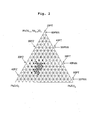
- the PNN-PT-PZ solid solution exhibits a relatively large strain (up to 0.12 %), and the solid solution exhibits a maximum piezoelectric constant d33 (stain amount with respect to unit voltage) in the vicinity of a composition of 50 molar % PNN-35 molar % PT-15 molar % PZ.
- the strain is changed in relation to the peak of the composition of 50 molar % PNN-35 molar % PT-15 molar % PZ in accordance with contour lines having such a certain pattern that the strain is decreased as the distance of separation from the peak is increased.
- An ink-jet head which is carried on an ink-jet printer, includes a piezoelectric type head which is constructed such that a piezoelectric actuator is arranged on a wall surface of an ink cavity,'and an ink contained in the ink cavity is discharged from an orifice by utilizing a strain generated when electric power is applied to the piezoelectric actuator.
- the piezoelectric ceramic composition which is composed of the PNN-PT-PZ solid solution as described above, can be used as the piezoelectric actuator of the ink-jet head.
- the PNN-PT-PZ solid solution exhibits the relatively large strain (up to 0.12 %) in the vicinity of the composition of 50 molar % PNN-35 molar % PT-15 molar % PZ.
- the relative dielectric constant is 5900 which is large.
- the input electric energy which is used to effect the high speed response of the piezoelectric actuator, is also increased.
- Such a phenomenon is not necessarily preferred for the head-driving circuit even when the strain amount of the piezoelectric actuator is large with respect to the electric field. For example, a problem arises such that the head-driving circuit is large-sized.
- the present invention has been made in order to solve the problems involved in the conventional technique as described above, an object of which is to provide a piezoelectric ceramic composition which makes it possible to bring about a large strain amount while suppressing the relative dielectric constant, and a piezoelectric actuator which is composed of such a piezoelectric ceramic composition and which is preferably usable for a variety of ways of use, especially for an ink-jet head.
- a piezoelectric ceramic composition comprising Pb(Ni 1/3 Nb 2/3 )O 3 , PbTiO 3 , and PbZrO 3 , wherein:
- the strain is further increased when the piezoelectric ceramic composition is composed of only Pb(Ni 1/3 Nb 2/3 )O 3 , PbTiO 3 , and PbZrO 3 .
- the composition of the present invention may further contain La in a ratio of 0.3 to 0.5 % by weight as calculated by conversion into an oxide represented by La 2 O 3 . In this case, it is possible to lower the mechanical quality factor (Q value) of the actuator and the sensor.
- a piezoelectric actuator which is formed of the piezoelectric ceramic composition of the present invention.
- the actuator of the present invention has a high degree of high speed response performance, and the actuator consumes less electric power, because the actuator is formed by using the composition of the present invention.
- an ink-jet head comprising the piezoelectric actuator of the present invention and a cavity plate.
- the ink-jet head makes it possible to perform high speed printing, the ink-jet head consumes less electric power, and the ink-jet head can be miniaturized, because the ink-jet head uses the piezoelectric actuator of the present invention.
- Fig. 1 illustrates a composition area of a piezoelectric ceramic composition according to an embodiment of the present invention as represented by a triangular coordinate system.
- Fig. 2 illustrates compositions corresponding to respective Sample Nos. 1 to 39 as depicted by the triangular coordinate system respectively.
- Fig. 3 shows magnified major portions shown in Fig. 2 and illustrates them while adding values of the piezoelectric displacement d33 as calculated by conversion into values of displacement amounts ( ⁇ m) per 1 mm at 1 kV corresponding to the respective compositions.
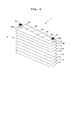
- Fig. 4 shows an expanded perspective view illustrating an ink-jet printer head.
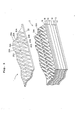
- Fig. 5 shows an expanded perspective view illustrating major portions of a cavity plate and a piezoelectric sheet of the ink-jet printer head.
- Fig. 6 shows schematic structures of a driving electrode and an ink pressure chamber of the ink-jet printer head, wherein Fig. 6A shows a plan view, and Fig. 6B shows a vertical sectional view.
- Fig. 7 shows a magnified perspective view of major portions schematically illustrating the structural arrangement of the driving electrodes formed on the piezoelectric sheet of the ink-jet printer head.
- Fig. 8 shows a magnified vertical sectional view illustrating major portions of the piezoelectric sheet of the ink-jet printer head.
- Fig. 9 shows an expanded perspective view schematically illustrating an electric connection structure in the piezoelectric sheet of the ink-jet printer head.
- Fig. 10 shows a graph illustrating an effect of an additive when La 2 O 3 is added to the piezoelectric ceramic composition.
- Fig. 1 illustrates a composition area of the piezoelectric ceramic composition according to the embodiment of the present invention as represented by a triangular coordinate system.
- the piezoelectric displacement d33 which is obtained when a DC electric field of 1 kV/mm is applied in the same direction as that of the polarization axis thereof, is not less than 750 pm/V.
- the relative dielectric constant of the piezoelectric ceramic composition having the composition described above at 1 kHz is within a range of 3550 to 1700.
- the value of the relative dielectric constant is maintained to be considerably low values.
- La may be contained in a ratio of 0 to 0.5 % by weight (except for 0) as calculated by conversion into an oxide represented by La 2 O 3 with respect to the main components of the piezoelectric ceramic composition described above. Accordingly, the mechanical quality factor (Qm) can be lowered while the high piezoelectric displacement d33 of not less than 750 pm/V is maintained and the value of the relative dielectric constant is maintained within the low value range described above. Accordingly, when a piezoelectric actuator for an ink-jet head is formed of the piezoelectric ceramic composition as described above, the actuator can be driven at a low voltage. Thus, it is possible to miniaturize the head-driving circuit.
- the piezoelectric ceramic composition according to this embodiment When the piezoelectric ceramic composition according to this embodiment is formed, starting materials of lead oxide (PbO), nickel oxide (NiO), niobium oxide (Nb 2 O 5 ), titanium oxide (TiO 2 ), and zirconium oxide (ZrO 2 ) are used. As for these materials, only lead oxide is weighed in an excessive amount, and the other oxides are weighed so that the stoichiometric ratio of the desired composition is obtained. The additive is weighed with respect to the total amount of the composition to be obtained after the sintering. After mixing the materials, the mixture is formed to have an appropriate form such as a tablet or a prism, and the heat treatment is performed preferably for 1 to 2 hours at 950 to 1050 °C in the atmospheric air.
- PbO lead oxide
- NiO nickel oxide
- niobium oxide Nb 2 O 5
- TiO 2 titanium oxide
- ZrO 2 zirconium oxide
- the method for mixing the materials is preferably exemplified by the dry mixing and the wet mixing.
- the forming method is preferably exemplified by the die press method and the wet press method.
- the heat treatment method is preferably exemplified by the heat treatment performed in the atmospheric air. However, there is no limitation thereto.
- the materials, which have been subjected to the heat treatment as described above, are treated as follows. That is, unreacted matters are dissolved with an aqueous acidic solution, for example, an aqueous acetic acid solution of 1 N. Particles are separated by means of the filtration operation. Subsequently, the obtained particles are formed by using a die press machine, followed by being sintered for 1 to 3 hours at 1200 to 1260 °C in a PbO atmosphere or in the atmospheric air to prepare a sintered product.
- the sintering means is exemplified, for example, by the ordinary sintering method and the pressurizing sintering method. However, there is no limitation thereto.
- Lead oxide (PbO), nickel oxide (NiO), niobium oxide (Nb 2 O 5 ), titanium oxide (TiO 2 ), and zirconium oxide (ZrO 2 ) were used as starting materials. As for these materials, only lead oxide was weighed in an excessive amount, and the other oxides were weighed so that the stoichiometric ratio of the desired composition was obtained.
- the mixture was formed to have a form of tablet, and the heat treatment was performed at 1050 °C for 1 hour in the atmospheric air.
- the dry mixing and the wet mixing were used in combination.
- the formed product after the heat treatment was treated as follows. That is, unreacted matters were dissolved with an aqueous acetic acid solution of 1 N, and particles were separated by means of the filtration operation, followed by being dried.
- the obtained particles were mixed with an appropriate amount of binder to form granules, followed by being formed into a disk having a diameter of 12 mm and a thickness of 2 mm by using a die press machine. After that, the sintering was performed for 3 hours at 1220 °C in the atmospheric air to prepare a sintered product.
- the disk-shaped sintered product was polished to have a thickness of 1 mm, and then silver electrodes were thermally formed and attached onto both surfaces to perform a polarization treatment for 30 minutes at 2 kV/mm in silicon oil.
- the polarization treatment was performed in a direction of the axis of rotation of the disk (thickness direction).
- Respective components Additive d33 (1 kV) pm•V -1 Remarks X X Y Y Z Z 1 44 36 20 - 680 * 2 42 38 20 - 700 * 3 42 36 22 - 660 * 4 42 32 26 - 700 * 5 41 35 24 - 700 * 6 40 40 20 - 620 * 7 40 39 21 - 620 * 8 40 38 22 - 720 * 9 40 37 23 - 820 10 40 36 24 - 620 * 11 40 35 25 - 660 * 12 40 34 26 - 640 * 13 40 32 28 - 600 * 14 39 39 22 - 640 * 15 39 38 23 - 800 16 39 37 24 - 780 17 38 40 22 - 720 * 18 38 39 23 - 800 19 38 38 24 - 1020 20 38 37 25 - 770 21 38 36 26 - 620 * 22 38 34 28 - 600 * 23 37 40 23 - 750 24 37 39 24 - 820 25 37 38 25 - 920 26 37 37 26 - 770 27 36 40 24
- any one of the values of the piezoelectric displacement d33 obtained with the compositions of Sample Nos. 1 to 8, 10 to 14, 17, 21, 22, 31, 34, 37, and 38 is not more than 750 pm/V, revealing that the values are not more than the threshold value.
- the value of the piezoelectric displacement d33 is not less than 750 pm/V (threshold value) in any one of the compositions in the vicinity of the substantial center of the peak value (1020 pm/V) of the piezoelectric displacement d33 obtained in the sample (Sample No.
- Point D Point D
- the value of the piezoelectric displacement d33 is not less than 800 pm/V (threshold value) in any one of the compositions on the lines for connecting the respective composition points of Point E (PNN: 38 molar %, PT: 38 molar %, PZ: 24 molar %, Sample No. 19)
- Point F Point F (PNN: 36 molar %, PT: 38 molar %, PZ: 26 molar %, Sample No.
- Point G (PNN: 35 molar %, PT: 39 molar %, PZ: 26 molar %, Sample No. 29), and Point H (PNN: 37 molar %, PT: 39 molar %, PZ: 24 molar %, Sample No. 24) and in the area surrounded by the four points.
- the dielectric characteristics were measured by using an impedance analyzer for the samples having the respective compositions included in the area surrounded by Point A, Point B, Point C, and Point D as described above. As a result, it has been confirmed that the relative dielectric constant at 1 kHz exists in a range of 3550 to 1700 in any one of the compositions, and the value of the relative dielectric constant is maintained to be relatively low values.
- the piezoelectric ceramic composition concerning Example 1 it is possible to realize the large strain amount in which the piezoelectric displacement d33 is not less than 750 pm/V while suppressing the relative dielectric constant to be low within the range of 3550 to 1700.
- a piezoelectric sheet which acts as a piezoelectric actuator for an ink-jet head, is formed of the piezoelectric ceramic composition prepared as described above, and the piezoelectric sheet is used for an ink-jet printer head.
- Fig. 4 shows an expanded perspective view illustrating the ink-jet printer head.
- Fig. 5 shows an expanded perspective view illustrating major portions of a cavity plate and the piezoelectric sheet of the ink-jet printer head.
- Fig. 6 shows schematic structures of a driving electrode and an ink pressure chamber of the ink-jet printer head, wherein Fig. 6A shows a plan view, and Fig. 6B shows a vertical sectional view.
- Fig. 7 shows a magnified perspective view of major portions schematically illustrating the structural arrangement of the driving electrodes formed on the piezoelectric sheet of the ink-jet printer head.
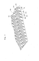
- the ink-jet printer head 1 has such a structure that respective five plate-shaped piezoelectric sheets 20, 20, 20, 20, 20, 20, which are substantially trapezoidal or substantially parallelogram-shaped as viewed in a plan view, are stacked in a mutually adjoining state on a cavity plate 2 which has a stacked structure composed of thin metal plates formed to be substantially rectangular.
- Ink pressure chambers 19A which are formed to be substantially lozenge-shaped, are arranged in a plurality of arrays on the surface of the cavity plate 2 corresponding to the required printing density.
- the respective ink pressure chambers 19A in the plurality of arrays are arranged at a high density so that acute angle portions of the ink pressure chambers 19A mutually enter the spaces between the ink pressure chambers on other arrays.
- the cavity plate 2 has a nine-lavered structure in which nine plate members, which are composed of substantially rectangular metal plates, are stacked. Specifically, as shown in Fig. 6B, the cavity plate 2 has a structure obtained by stacking the nine thin metal plates, i.e., a nozzle plate 11, a cover plate 12, a first manifold plate 13, a second manifold plate 14, a third manifold plate 15, a supply plate 16, an aperture plate 17, a spacer plate 18, and a base plate 19 in this order from the bottom layer. As shown in Fig. 4, respective filter holes 19B, 19B, to which the ink is supplied, are formed at both end edge portions of the cavity plate 2 in the longitudinal direction. Respective filters 21, 21, through which a large number of fine through-holes are formed in order to prevent any invasion of dust contained in the ink, are stacked on the respective filter holes 19B, 19B.
- a large number of ink-jetting nozzles 11A are bored through the nozzle plate 11.
- a large number of through-holes 12A which serve as ink passages having minute diameters communicating with the nozzles 11A, are bored through the cover plate 12 at positions opposed to the respective nozzles 11A.
- the cover plate 12 constitutes one wall surface of the ink manifold passage formed by the respective manifold plates 13, 14, 15 as described later on.
- the ink manifold passages which are constituted by the upper surface portions of the cover plate 12, the respective groove-shaped holes 13B, 14B, 15B, and the bottom surface portions of the supply plate 16 and which serve as common ink chambers for supplying the ink to the respective ink pressure chambers 19A, are formed in a plurality of arrays in the longitudinal direction.
- the aperture plate 17 has through-holes 17B which are bored at positions under the acute angle portions disposed on the ink supply side of the respective ink pressure chambers 19A.
- aperture sections 17C which are groove-shaped recesses, are formed on the bottom surface from the lower ends of the through-holes 17B to positions opposed to the through-holes 16B.
- the aperture sections 17C are formed as grooves each having a depth of about a half of the thickness of the aperture plate 17.
- the large number of substantially lozenge-shaped ink pressure chambers 19A are formed through the base plate 19.
- the respective through-holes 18A, 18B, which are bored through the spacer plate 18, are arranged so that they are opposed to the respective acute angle portions of the ink pressure chambers 19A.
- the upper surfaces of the respective ink pressure chambers 19A are closed by the respective piezoelectric sheets 20, 20, 20, 20, 20 stacked thereon.
- Driving electrodes 20A which have substantially similar lozenge-shaped configurations slightly smaller than projected configurations of the lozenge-shaped ink pressure chambers 19A, are formed at positions corresponding to the respective ink pressure chambers 19A on the upper surfaces of the piezoelectric sheets 20. As shown in Fig. 6A, an arrow-shaped land pattern 20B is formed continuously to the acute angle portion of the driving electrode 20A corresponding to the acute angle portion disposed on the ink supply side of each of the ink pressure chambers 19A.
- Figs. 8 and 9 show a schematic structure of the piezoelectric sheet 20 and an electric connection structure with respect to a flexible printed circuit board (FPC) provided to extend from a power source circuit unit (not shown).
- Fig. 8 shows a magnified vertical sectional view illustrating major portions of the piezoelectric sheet 20 of the ink-jet printer head 1.
- Fig. 9 shows an expanded perspective view schematically illustrating the electric connection structure in the piezoelectric sheet 20 of the ink-jet printer head 1.
- the piezoelectric sheet 20 is formed to have such a structure that five layers, i.e., a first piezoelectric layer 21, a second piezoelectric layer 22, a third piezoelectric layer 23, a fourth piezoelectric layer 24, and a fifth piezoelectric layer 25 are stacked.
- the substantially lozenge-shaped driving electrode 20A having an approximately similar shape slightly smaller than the projected shape of the ink pressure chamber 19A, and the arrow-shaped land pattern 20B formed continuously to the acute angle portion of the driving electrode 20A are formed at positions corresponding to each of the ink pressure chambers 19A as described above on the upper surface of the first piezoelectric layer 21.
- a through-hole 20C is bored through a substantially central portion of each of the land patterns 20B.
- a large number of through-holes 22A are bored through the second piezoelectric layer 22 at positions opposed to the through-holes 20C.
- a common electrode 22B is formed on the substantially entire upper surface of the second piezoelectric layer 22 except for positions in the vicinity of upper end circumferential edge portions of the respective through-holes 22A.
- the common electrode 22B has its end which is formed to be exposed to the side surface end of the second piezoelectric layer 22.
- a large number of internal electrodes 23A which have approximately the same shapes as those of the driving electrodes 20A and the land patterns 20B, are formed at positions corresponding to the respective driving electrodes 20A and the land patterns 20B on the upper surface of the third piezoelectric layer 23.
- a common electrode 24A is formed on the substantially entire upper surface of the fourth piezoelectric layer 24.
- the common electrode 24A has its end which is formed to be exposed to the side surface end of the fourth piezoelectric layer 24.
- No electrode is formed on the upper surface of the fifth piezoelectric layer 25.
- the respective through-holes 20C of the first piezoelectric layer 21 are communicated with the respective through-holes 22A of the second piezoelectric layer 22 to form the respective through-holes 30.
- the respective through-holes 30 are filled with a conductive material (for example, tungsten or molybdenum). Accordingly, the respective land patterns 20B are electrically connected to the respective internal electrodes 23A via the through-holes 30.
- the flexible printed circuit board (FPC) 32 which is provided to extend from the unillustrated power source circuit unit, is arranged on the upper surface of the piezoelectric sheet 20.
- FPC 32 comprises conductor sections 33 which are composed of copper foils wired up to positions opposed to the respective land patterns 20B, a base film 34 which is bonded to the upper surfaces of the conductor sections 33, and a cover film 35 which is bonded to the lower surfaces of the conductor sections 33.
- a large number of through-holes 35A are bored at positions of the cover film 35 opposed to the respective land patterns 20B, i.e., at end edge portions of the respective conductor sections 33.
- Preparatory solder pieces 36 which are disposed to make the connection to the respective land patterns 20B, are formed at portions of the conductor sections 33 corresponding to the respective through-holes 35A.
- each of the portions of the first to third piezoelectric layers 21, 22, 23, which corresponds to the driving electrode 20A and the internal electrode 23A, constitutes the active section which is flexibly bent when the voltage is applied.
- the entire sheet may become warped or wavy in some cases, because the coefficient of contraction differs between the piezoelectric ceramics and the metal material for constructing the electrode when the sintering is performed.
- the fourth and fifth piezoelectric layers 24, 25 function as constraint layers in order that the flatness is not deteriorated for the first to fifth piezoelectric layers 21, 22, 23, 24, 25 as a result of the warpage or the wavy form after the sintering, and in order that the active sections of the first to third piezoelectric layers 21, 22, 23 are deformed in only the direction toward the ink pressure chamber 19A.
- the ink which is supplied from the ink manifold passage constructed by the upper surface of the cover plate 12, the respective groove-shaped holes 13B, 14B, 15B, and the bottom surface of the supply plate 16, passes through the through-hole 16B, the aperture section 17C, the through-hole 17B, and the through-hole 18B, and the ink flows into the ink pressure chamber 19A.
- the driving voltage is applied between the land pattern 20B and the respective common electrodes 22B, 24B by the aid of FPC 32, then the piezoelectric sheet 20 is deformed toward the ink pressure chamber 19A, and the ink contained in the ink pressure chamber 19A is extruded.
- the ink is discharged from the nozzle 11A via the respective through-holes 18A, 17A, 16A, 15A, 14A, 13A, 12A.
- the driving voltage was successfully lowered by about 35 % as compared with a conventional case in which a printer head having the same structure as the ink-jet printer head except for piezoelectric layers being formed of conventional piezoelectric ceramic composition was used.
- the conventional piezoelectric composition has the piezoelectric displacement d33 of 600-650 pm/V. Accordingly, the piezoelectric sheet 20 (piezoelectric actuator for the ink-jet head) formed of the piezoelectric ceramic composition described above can be driven at a lower voltage. It is possible to miniaturize the head-driving circuit, and it is oossible to increase the degree of freedom of the design of the head-driving circuit.
- the piezoelectric sheet 20 piezoelectric actuator for the ink-jet head formed of the piezoelectric ceramic composition described above
- the driving operation can be performed at a lower voltage, and it is possible to realize a small size of the head-driving circuit.
- the piezoelectric sheet 20 when used, the displacement can be obtained as required'even when the active section corresponding to the driving electrode 20A and the internal electrode 23A is narrowed. Accordingly, it is possible to make the head-driving circuit to be finer, and it is possible to realize a high density.
- the relative dielectric constant can be made to be relatively low within a range of 3550 to 1700. Therefore, the response characteristics are improved with respect to the input signal, and it is possible to perform the driving at a high speed. Further, it is possible to suppress any useless electric power consumption, and it is possible to increase the degree of freedom of the design of the head-driving circuit.
- Fig. 10 shows a graph illustrating an effect of an additive when La 2 O 3 is added to the piezoelectric ceramic composition.
- the vertical axis indicates the mechanical quality factor Qm
- the horizontal axis indicates the amount of addition of La 2 O 3 (% by weight).
- a piezoelectric ceramic composition according to Example 2 was prepared in the same manner as in Example 1 except that La 2 O 3 as an additive was weighed and mixed in an objective amount based on the composition to be obtained after the sintering, in addition to lead oxide (PbO), nickel oxide (NiO), niobium oxide (Nb 2 O 5 ), titanium oxide (TiO 2 ), and zirconium oxide (ZrO 2 ) as the starting materials, and the sintering was performed at 1260 °C for 3 hours when the respective materials were sintered.
- PbO lead oxide
- NiO nickel oxide
- Nb 2 O 5 niobium oxide
- TiO 2 titanium oxide
- ZrO 2 zirconium oxide
- the piezoelectric ceramic composition according to Example 2 is represented by Sample Nos. 40 to 43 shown in Table 1.
- the basic composition of PNN-PT-PZ was the composition including PNN of 37 molar %, PT of 38 molar %, and PZ of 25 molar % (Sample No. 25) in which the relatively high piezoelectric displacement d33 was obtained in the area surrounded by Point A, Point B, Point C, and Point D as described above, to which La 2 O 3 was added by 0.1 % by weight (Sample No. 40), 0.3 % by weight (Sample No. 41), 0.5 % by weight (Sample No. 42), and 1.0 % by weight (Sample No. 43) respectively.
- the values of the piezoelectric displacement d33 any one of which was not less than 750 pm/V as the threshold value, were measured in the same manner as described above for Sample 40 in which La 2 O 3 was added by 0.1 % by weight, Sample 41 in which La 2 O 3 was added by 0.3 % by weight, and Sample 42 in which La 2 O 3 was added by 0.5 % by weight.
- the value of the piezoelectric displacement d33 which was measured for Sample 43 in which La 2 O 3 was added by 1.0 % by weight, was 740 pm/V which was not more than the threshold value (750 pm/V).
- the dielectric characteristics were measured for Samples 40 to 43 by using an impedance analyzer in the same manner as in Example 1. As a result, the relative dielectric constants at 1 kHz were 3100 to 3300 for Samples 40 to 42, but a relatively high value of 3700 was measured for Sample 43.
- the relationship between the mechanical quality factor Qm and the amount of addition of La 2 O 3 was measured for respective Samples 40 to 43.
- the mechanical quality factor Qm is slightly lowered when the amount of addition of La 2 O 3 is 0.1 % by weight, and Qm is suddenly lowered when the amount of addition of La 2 O 3 is increased up to 0.3 % by weight.
- the decrease in mechanical quality factor Qm is extremely small even when the amount of addition of La 2 O 3 is increased from 0.3 % by weight to 0.5 % by weight, and this tendency is scarcely changed even when the amount of addition of La 2 O 3 is increased up to 1.0 % by weight.
- the mechanical quality factor Qm when La 2 O 3 is added to the piezoelectric ceramic composition, the mechanical quality factor Qm can be effectively lowered in a range in which the amount of addition is 0.1 % by weight to 0.5 % by weight. In particular, the mechanical quality factor Qm can be lowered more effectively when the amount of addition is in a range of 0.3 % by weight to 0.5 % by weight.
- the resonance frequency approaches the antiresonance frequency, which is preferred for the way of use, for example, for actuators and sensors.
- a piezoelectric sheet to act as the piezoelectric actuator for the ink-jet head was formed of the piezoelectric ceramic composition according to Example 2 prepared as described above, and an ink-jet printer head, which was manufactured in the same manner as in Example 1 by using the piezoelectric sheet as described above, was subjected to the head driving by using the conventional head-driving circuit.
- the driving voltage was successfully lowered by about 35 % as compared with the conventional technique.
- the piezoelectric sheet 20 piezoelectric actuator for the ink-jet head
- the piezoelectric sheet 20 which is formed of the piezoelectric ceramic composition described above, can be driven at a lower voltage. It is possible to miniaturize the head-driving circuit, and it is possible to increase the degree of freedom of the design of the head-driving circuit.
- the piezoelectric sheet 20 piezoelectric actuator for the ink-jet head
- the driving operation can be performed at a lower voltage, and it is possible to realize a small size of the head-driving circuit.
- the piezoelectric sheet 20 when the piezoelectric sheet 20 is used, the displacement can be obtained as required even when the active section corresponding to the driving electrode 20A and the internal electrode 23A is narrowed. Accordingly, it is possible to make the head-driving circuit to be finer, and it is possible to realize a high density.
- the relative dielectric constant can be made to be relatively low within a range of 3100 to 3300. Therefore, the response characteristics are improved with respect to the input signal, and it is possible to perform the driving at a high speed. Further, it is possible to suppress any useless electric power consumption, and it is possible to increase the degree of freedom of the design of the head-driving circuit.
- the composition of the present invention is preferably usable, for example, for piezoelectric ceramic materials which are used, for example, for ultrasonic vibrators, piezoelectric relays, piezoelectric valves, flow rate sensors, acceleration sensors, and autofocusing lens actuators used for cameras and optical recording apparatuses.
- the composition of the present invention is preferably usable for stacked type piezoelectric element materials such as piezoelectric actuators for the ink-jet head.
Landscapes
- Chemical & Material Sciences (AREA)
- Engineering & Computer Science (AREA)
- Ceramic Engineering (AREA)
- Manufacturing & Machinery (AREA)
- Materials Engineering (AREA)
- Structural Engineering (AREA)
- Organic Chemistry (AREA)
- Composite Materials (AREA)
- Particle Formation And Scattering Control In Inkjet Printers (AREA)
- Compositions Of Oxide Ceramics (AREA)
Applications Claiming Priority (2)
| Application Number | Priority Date | Filing Date | Title |
|---|---|---|---|
| JP2002219568 | 2002-07-29 | ||
| JP2002219568A JP2004059369A (ja) | 2002-07-29 | 2002-07-29 | 圧電磁器組成物及びこれを用いたインクジェットヘッド用圧電アクチュエータ |
Publications (2)
| Publication Number | Publication Date |
|---|---|
| EP1400498A2 true EP1400498A2 (fr) | 2004-03-24 |
| EP1400498A3 EP1400498A3 (fr) | 2004-06-09 |
Family
ID=31940437
Family Applications (1)
| Application Number | Title | Priority Date | Filing Date |
|---|---|---|---|
| EP03254745A Withdrawn EP1400498A3 (fr) | 2002-07-29 | 2003-07-29 | Composition céramique piézoélectrique et actionneur piézoélectrique pour tête à jet d'encre |
Country Status (3)
| Country | Link |
|---|---|
| US (1) | US6844661B2 (fr) |
| EP (1) | EP1400498A3 (fr) |
| JP (1) | JP2004059369A (fr) |
Cited By (1)
| Publication number | Priority date | Publication date | Assignee | Title |
|---|---|---|---|---|
| EP1901361A3 (fr) * | 2006-09-15 | 2009-08-05 | Fujifilm Corporation | Oxyde pérovskite, processus de production d'oxyde pérovskite, corps piézoélectrique, dispositif piézoélectrique, et dispositif de libération liquide |
Families Citing this family (5)
| Publication number | Priority date | Publication date | Assignee | Title |
|---|---|---|---|---|
| KR100480876B1 (ko) * | 2001-11-15 | 2005-04-07 | (주)아이블포토닉스 | 신규의 압전 단결정을 이용한 초음파 탐촉자 |
| JP2006310746A (ja) | 2005-03-30 | 2006-11-09 | Seiko Epson Corp | 圧電素子並びに圧電素子を用いた液体噴射ヘッド及び液体噴射装置 |
| JP5290551B2 (ja) * | 2006-09-15 | 2013-09-18 | 富士フイルム株式会社 | ペロブスカイト型酸化物とその製造方法、圧電体、圧電素子、液体吐出装置 |
| PL2345355T3 (pl) * | 2006-12-06 | 2013-10-31 | Rheavendors Services Spa | Sposób i maszyna do wytwarzania i dozowania napojów |
| US11133179B2 (en) | 2019-11-27 | 2021-09-28 | Samsung Electronics Co., Ltd. | Thin-film structure and method of manufacturing the same |
Family Cites Families (16)
| Publication number | Priority date | Publication date | Assignee | Title |
|---|---|---|---|---|
| JPS5915503B2 (ja) * | 1974-11-21 | 1984-04-10 | 日本電気株式会社 | ジルコン・チタン酸鉛を含む多成分系圧電性磁器用結晶化微粉末の製造方法 |
| JPS63225577A (ja) | 1987-03-13 | 1988-09-20 | 岩崎通信機株式会社 | 圧電磁器組成物 |
| JPS63285167A (ja) | 1987-05-15 | 1988-11-22 | Iwatsu Electric Co Ltd | 圧電磁器組成物 |
| JPS645973A (en) | 1987-06-27 | 1989-01-10 | Iwatsu Electric Co Ltd | Piezoelectric porcelain composition |
| JPH0558645A (ja) | 1991-09-03 | 1993-03-09 | Hitachi Metals Ltd | 圧電磁器組成物 |
| DE4402420C2 (de) * | 1993-01-27 | 1996-03-28 | Toshiba Kawasaki Kk | Piezoelektrisches Material und Ultraschallsonde |
| JP2674576B2 (ja) * | 1995-07-28 | 1997-11-12 | 日本電気株式会社 | 圧電磁器組成物 |
| JP3890634B2 (ja) * | 1995-09-19 | 2007-03-07 | セイコーエプソン株式会社 | 圧電体薄膜素子及びインクジェット式記録ヘッド |
| JP3044304B1 (ja) * | 1998-12-28 | 2000-05-22 | 工業技術院長 | 高性能圧電セラミックスおよびその製造方法 |
| JP2001002469A (ja) * | 1999-04-22 | 2001-01-09 | Murata Mfg Co Ltd | 圧電体ペーストならびにこれを用いた圧電体膜および圧電体部品 |
| JP2001178159A (ja) * | 1999-10-08 | 2001-06-29 | Denso Corp | 超音波モータとその製造方法 |
| JP3934324B2 (ja) * | 1999-10-29 | 2007-06-20 | Tdk株式会社 | 圧電セラミックス |
| JP2001302348A (ja) | 2000-04-19 | 2001-10-31 | Tokin Corp | 圧電磁器組成物 |
| JP2001302350A (ja) | 2000-04-19 | 2001-10-31 | Tokin Corp | 圧電磁器組成物 |
| JP2001302349A (ja) | 2000-04-19 | 2001-10-31 | Tokin Corp | 圧電磁器組成物 |
| JP2002226266A (ja) | 2001-01-30 | 2002-08-14 | Nec Tokin Corp | 圧電磁器組成物 |
-
2002
- 2002-07-29 JP JP2002219568A patent/JP2004059369A/ja active Pending
-
2003
- 2003-07-24 US US10/625,747 patent/US6844661B2/en not_active Expired - Lifetime
- 2003-07-29 EP EP03254745A patent/EP1400498A3/fr not_active Withdrawn
Cited By (3)
| Publication number | Priority date | Publication date | Assignee | Title |
|---|---|---|---|---|
| EP1901361A3 (fr) * | 2006-09-15 | 2009-08-05 | Fujifilm Corporation | Oxyde pérovskite, processus de production d'oxyde pérovskite, corps piézoélectrique, dispositif piézoélectrique, et dispositif de libération liquide |
| US7918542B2 (en) | 2006-09-15 | 2011-04-05 | Fujifilm Corporation | Perovskite oxide, process for producing the perovskite oxide, piezoelectric body, piezoelectric device, and liquid discharge device |
| US8434856B2 (en) | 2006-09-15 | 2013-05-07 | Fujifilm Corporation | Perovskite oxide, process for producing the perovskite oxide, piezoelectric body, piezoelectric device, and liquid discharge device |
Also Published As
| Publication number | Publication date |
|---|---|
| US6844661B2 (en) | 2005-01-18 |
| EP1400498A3 (fr) | 2004-06-09 |
| JP2004059369A (ja) | 2004-02-26 |
| US20040119378A1 (en) | 2004-06-24 |
Similar Documents
| Publication | Publication Date | Title |
|---|---|---|
| US5912526A (en) | Layered-type piezoelectric element and method for producing the layered-type piezoelectric element | |
| KR100651046B1 (ko) | 유전체막 구조체, 유전체막 구조체를 사용하는 압전액추에이터 및 잉크젯 헤드 | |
| US7576477B2 (en) | Piezoelectric/electrostrictive porcelain composition and method of manufacturing the same | |
| US9318690B2 (en) | Piezoelectric element, liquid ejecting head, and liquid ejecting apparatus | |
| US7521845B2 (en) | Piezoelectric substance, piezoelectric element, liquid discharge head using piezoelectric element, and liquid discharge apparatus | |
| US6891316B2 (en) | Laminated piezoelectric element, actuator and printing head | |
| EP1770798B1 (fr) | Actionneur piézoélectrique, son procède de fabrication et tête d'écriture à jet d'encre | |
| US7677708B2 (en) | Discharge device | |
| US6844661B2 (en) | Piezoelectric ceramic composition and piezoelectric actuator for ink-jet head based on use of the same | |
| JP4875827B2 (ja) | 圧電薄膜及びその製造方法、並びにその圧電薄膜を備えた圧電素子、並びにその圧電素子を用いたインクジェットヘッド、並びにそのインクジェットヘッドを備えたインクジェット式記録装置 | |
| JP5458085B2 (ja) | 積層圧電体、圧電アクチュエータおよび印刷ヘッド | |
| JP4812244B2 (ja) | 印刷ヘッド | |
| JP5260900B2 (ja) | 液体吐出ヘッド | |
| JP3319413B2 (ja) | 圧電アクチュエータ、圧電アクチュエータの製造方法及びインクジェットヘッド | |
| JP4307161B2 (ja) | 印刷ヘッド及び電子機器 | |
| JP5096659B2 (ja) | 圧電アクチュエータおよび印刷ヘッド | |
| CN101070005B (zh) | 促动器及其制造方法以及打印头 | |
| EP1582353B1 (fr) | Appareil d'éjection de liquide, appareil d'enregistrement, et tête d'impression par jet d'encre | |
| JP2008244135A (ja) | 液体吐出ヘッド用積層圧電アクチュエータおよびその製造方法ならびに液体吐出ヘッド | |
| JP4833510B2 (ja) | インクジェット記録ヘッドおよびその製造方法 | |
| JP2007267550A (ja) | 圧電アクチュエータおよびその分極方法 | |
| JP2004142350A (ja) | アクチュエータ及び印刷ヘッド | |
| JP2005244091A (ja) | 圧電積層体、圧電アクチュエータ、印刷ヘッドおよび印刷機 | |
| JP2006237077A (ja) | 積層圧電体及び圧電アクチュエータ | |
| JP2000177130A (ja) | インクジェットヘッド及びそのアクチュエ―タアレイの製造方法 |
Legal Events
| Date | Code | Title | Description |
|---|---|---|---|
| PUAI | Public reference made under article 153(3) epc to a published international application that has entered the european phase |
Free format text: ORIGINAL CODE: 0009012 |
|
| AK | Designated contracting states |
Kind code of ref document: A2 Designated state(s): AT BE BG CH CY CZ DE DK EE ES FI FR GB GR HU IE IT LI LU MC NL PT RO SE SI SK TR |
|
| AX | Request for extension of the european patent |
Extension state: AL LT LV MK |
|
| PUAL | Search report despatched |
Free format text: ORIGINAL CODE: 0009013 |
|
| AK | Designated contracting states |
Kind code of ref document: A3 Designated state(s): AT BE BG CH CY CZ DE DK EE ES FI FR GB GR HU IE IT LI LU MC NL PT RO SE SI SK TR |
|
| AX | Request for extension of the european patent |
Extension state: AL LT LV MK |
|
| RIC1 | Information provided on ipc code assigned before grant |
Ipc: 7H 01L 41/187 B Ipc: 7C 04B 35/493 B Ipc: 7C 04B 35/499 A |
|
| 17P | Request for examination filed |
Effective date: 20041206 |
|
| AKX | Designation fees paid |
Designated state(s): AT BE BG CH CY CZ DE DK EE ES FI FR GB GR HU IE IT LI LU MC NL PT RO SE SI SK TR |
|
| 17Q | First examination report despatched |
Effective date: 20050513 |
|
| 17Q | First examination report despatched |
Effective date: 20050513 |
|
| STAA | Information on the status of an ep patent application or granted ep patent |
Free format text: STATUS: THE APPLICATION IS DEEMED TO BE WITHDRAWN |
|
| 18D | Application deemed to be withdrawn |
Effective date: 20071002 |