EP1406290A2 - Ablenkvorrichtung, Verfahren zu deren Herstellung und Belichtungsgerät für geladene Teilchen - Google Patents
Ablenkvorrichtung, Verfahren zu deren Herstellung und Belichtungsgerät für geladene Teilchen Download PDFInfo
- Publication number
- EP1406290A2 EP1406290A2 EP20030256205 EP03256205A EP1406290A2 EP 1406290 A2 EP1406290 A2 EP 1406290A2 EP 20030256205 EP20030256205 EP 20030256205 EP 03256205 A EP03256205 A EP 03256205A EP 1406290 A2 EP1406290 A2 EP 1406290A2
- Authority
- EP
- European Patent Office
- Prior art keywords
- substrate
- deflection electrode
- insulating layer
- conductive member
- charged particle
- Prior art date
- Legal status (The legal status is an assumption and is not a legal conclusion. Google has not performed a legal analysis and makes no representation as to the accuracy of the status listed.)
- Granted
Links
Images


Classifications
-
- H—ELECTRICITY
- H01—ELECTRIC ELEMENTS
- H01J—ELECTRIC DISCHARGE TUBES OR DISCHARGE LAMPS
- H01J37/00—Discharge tubes with provision for introducing objects or material to be exposed to the discharge, e.g. for the purpose of examination or processing thereof
- H01J37/02—Details
- H01J37/04—Arrangements of electrodes and associated parts for generating or controlling the discharge, e.g. electron-optical arrangement or ion-optical arrangement
- H01J37/045—Beam blanking or chopping, i.e. arrangements for momentarily interrupting exposure to the discharge
-
- B—PERFORMING OPERATIONS; TRANSPORTING
- B82—NANOTECHNOLOGY
- B82Y—SPECIFIC USES OR APPLICATIONS OF NANOSTRUCTURES; MEASUREMENT OR ANALYSIS OF NANOSTRUCTURES; MANUFACTURE OR TREATMENT OF NANOSTRUCTURES
- B82Y10/00—Nanotechnology for information processing, storage or transmission, e.g. quantum computing or single electron logic
-
- B—PERFORMING OPERATIONS; TRANSPORTING
- B82—NANOTECHNOLOGY
- B82Y—SPECIFIC USES OR APPLICATIONS OF NANOSTRUCTURES; MEASUREMENT OR ANALYSIS OF NANOSTRUCTURES; MANUFACTURE OR TREATMENT OF NANOSTRUCTURES
- B82Y40/00—Manufacture or treatment of nanostructures
-
- H—ELECTRICITY
- H01—ELECTRIC ELEMENTS
- H01J—ELECTRIC DISCHARGE TUBES OR DISCHARGE LAMPS
- H01J37/00—Discharge tubes with provision for introducing objects or material to be exposed to the discharge, e.g. for the purpose of examination or processing thereof
- H01J37/02—Details
- H01J37/04—Arrangements of electrodes and associated parts for generating or controlling the discharge, e.g. electron-optical arrangement or ion-optical arrangement
- H01J37/147—Arrangements for directing or deflecting the discharge along a desired path
- H01J37/1472—Deflecting along given lines
- H01J37/1474—Scanning means
- H01J37/1477—Scanning means electrostatic
-
- H—ELECTRICITY
- H01—ELECTRIC ELEMENTS
- H01J—ELECTRIC DISCHARGE TUBES OR DISCHARGE LAMPS
- H01J37/00—Discharge tubes with provision for introducing objects or material to be exposed to the discharge, e.g. for the purpose of examination or processing thereof
- H01J37/30—Electron-beam or ion-beam tubes for localised treatment of objects
- H01J37/317—Electron-beam or ion-beam tubes for localised treatment of objects for changing properties of the objects or for applying thin layers thereon, e.g. for ion implantation
- H01J37/3174—Particle-beam lithography, e.g. electron beam lithography
-
- H—ELECTRICITY
- H01—ELECTRIC ELEMENTS
- H01J—ELECTRIC DISCHARGE TUBES OR DISCHARGE LAMPS
- H01J2237/00—Discharge tubes exposing object to beam, e.g. for analysis treatment, etching, imaging
- H01J2237/04—Means for controlling the discharge
- H01J2237/043—Beam blanking
- H01J2237/0435—Multi-aperture
- H01J2237/0437—Semiconductor substrate
-
- H—ELECTRICITY
- H01—ELECTRIC ELEMENTS
- H01J—ELECTRIC DISCHARGE TUBES OR DISCHARGE LAMPS
- H01J2237/00—Discharge tubes exposing object to beam, e.g. for analysis treatment, etching, imaging
- H01J2237/30—Electron or ion beam tubes for processing objects
- H01J2237/317—Processing objects on a microscale
- H01J2237/3175—Lithography
- H01J2237/31774—Multi-beam
Definitions
- the present invention relates to a charged particle beam exposure apparatus which exposes the pattern of a semiconductor integrated circuit or the like onto a wafer and, more particularly, to a deflector in a charged particle beam exposure apparatus which exposes a pattern by using a plurality of charged particle beams and a method of manufacturing the deflector.
- Electron beam exposure apparatuses inherently ensure a high resolution and also have satisfactory dimension controllability as compared to other exposure means. Since the electron beam exposure apparatuses can electrically generate an exposure pattern and directly expose a wafer, they are expected as maskless exposure means.
- the exposure area per shot is small, and the throughput is low. For these reasons, they are not widely used for mass production of semiconductor devices.
- a multi-electron beam exposure apparatus which exposes a wafer by using a plurality of electron beams simultaneously has been proposed.
- Such a multi-electron beam exposure apparatus comprises a blanking aperture array device which switches a plurality of electron beams between an independent deflection mode and another mode, and an electron beam shielding section which shields the wafer from the electron beams deflected by the blanking aperture array device. With these units, whether the wafer is to be irradiated with each of the plurality of electron beams is accurately controlled.
- the blanking aperture array device has a substrate such as a semiconductor substrate having a plurality of openings (also called through holes), deflection electrodes formed in the openings, and an insulating layer which insulates the substrate from the deflection electrodes. Whether an electron beam that passes through an opening is to be deflected is controlled by ON/OFF-controlling voltage application to the deflection electrode.
- openings each having a high aspect ratio are formed in a substrate.
- a deflection electrode is formed in each of the openings by plating. Since the deflection electrode is formed by plating in the opening having a high aspect ratio, a material whose plating growth rate is low cannot be selected as the material of the deflection electrode. In addition, if the deflection electrode is oxidized, it becomes difficult to appropriately deflect an electron beam and control its position. To prevent this, a material that is hard to oxidize must be selected as the material of the deflection electrode. It is difficult to select the deflection electrode material that meets the above requirements.
- the substrate or insulating layer is partially exposed to the inner wall of each opening through which an electron beam passes. For this reason, the oxide film of the substrate or the insulating layer, which is exposed to the inner wall of the opening, is charged up and affects the electron beam that passes through the opening. Accordingly, the electron beam cannot be appropriately deflected or position-controlled. Hence, it is difficult to accurately expose the wafer.
- openings are formed in a substrate, and an insulating layer is formed on the inner wall of each opening.
- a deflection electrode is formed by plating using a conductive layer formed on the surface of the substrate as an electrode.
- the deflection electrode has residual stress and therefore poor adhesion to the insulating layer. For this reason, the deflection electrode readily peels off from the insulating layer.
- a deflector which deflects a charged particle beam, comprising: a substrate having an opening through which the charged particle beam should pass; and a deflection electrode which is arranged in the opening to deflect the charged particle beam and has a first conductive member and second conductive member which are formed by plating, wherein the second conductive member is formed on a surface of the first conductive member and is essentially made of a material that is more difficult to oxidize than the first conductive member.
- the word “essentially” in such phrases as “essentially made of a material that is more difficult to oxidise”, “essentially made of a material having a higher plating growth rate”, “essentially made of a material having smaller residual stress” etc may mean that the component concerned has a composition which itself has the relevant property.
- “essentially made of” may mean “is overwhelmingly composed of”, such as being at least 90%, or even at least 99%, composed of the stated material.
- a deflector which deflects a charged particle beam, comprising: a substrate having an opening through which the charged particle beam should pass; a first deflection electrode and second deflection electrode which oppose each other in the opening to deflect the charged particle beam; and a first conductive layer and second conductive layer which oppose each other in the opening in a direction substantially perpendicular to a direction from the first deflection electrode to the second deflection electrode and are made of a material having a higher conductivity than the substrate.
- a deflector which deflects a charged particle beam, comprising: a substrate having a through hole through which the charged particle beam should pass and two groove portions respectively formed on two opposing side surfaces inside the through hole; and two deflection electrodes which are at least partially buried in the two groove portions, wherein each of the groove portions has a shape to lock the buried portion of the deflection electrode in the groove portion to prevent the deflection electrode from separating from the substrate.
- Fig. 1 shows the arrangement of an electron beam exposure apparatus 100 according to the first embodiment.
- the electron beam exposure apparatus 100 is an example of the charged particle beam exposure apparatus of the present invention.
- the charged particle beam exposure apparatus of the present invention may be an ion beam exposure apparatus which exposes a wafer by an ion beam.
- the electron beam exposure apparatus 100 may generate a plurality of electron beams at a short interval and, for example, at such an interval that one chip region to be formed on a wafer is irradiated with all electron beams.
- the electron beam exposure apparatus 100 comprises an exposure section 150 which executes predetermined exposure processing for a wafer 44 by electron beams and a control section 140 which controls the operations of components included in the exposure section 150.
- the exposure section 150 comprises an electron optical system and a stage system.
- the electron optical system includes an electron beam shaping means 110 for generating a plurality of electron beams in a housing 8 and forming the sectional shape of each electron beam into a desired shape, an irradiation switching means 112 for independently switching for each of the plurality of electron beams whether the wafer 44 should be irradiated with the electron beam, and a wafer projecting system 114 which adjusts the direction and size of the image of a pattern to be transferred to the wafer 44.
- the stage system has a wafer stage 46 on which the wafer 44 to which the pattern is to be exposed is placed and a wafer stage driving section 48 which drives the wafer stage 46.
- the electron beam shaping means 110 has an electron beam generation section 10 which generates the plurality of electron beams, a first shaping member 14 and second shaping member 22 each of which has a plurality of opening portions that shape the sectional shapes of the electron beams, a first multi-axis electron lens 16 which independently focuses the plurality of electron beams and adjusts the focal points of the electron beams, and a first shaping deflecting section 18 and second shaping deflecting section 20 each of which independently deflects the plurality of electron beams that have passed through the first shaping member 14.
- the electron beam generation section 10 is an example of the charged particle beam generation section of the present invention.
- the first shaping deflecting section 18 and second shaping deflecting section 20 are examples of the deflector of the present invention.
- the electron beam generation section 10 has a plurality of electron guns 104 and a base 106 on which the electron guns 104 are formed.
- Each electron gun 104 has a cathode 12 which generates thermoelectrons and a grid 102 which is formed around the cathode 12 to stabilize the thermoelectrons generated by the cathode 12.
- the plurality of electron guns 104 are formed on the base 106 at a predetermined interval so that an electron gun array is formed.
- Each of the first shaping member 14 and second shaping member 22 preferably has a grounded metal film of platinum or the like on the surface that is irradiated with the electron beams.
- Each of the plurality of opening portions included in the first shaping member 14 and second shaping member 22 may have a sectional shape that extends along the electron beam irradiation direction to efficiently pass the electron beam.
- the plurality of opening portions included in the first shaping member 14 and second shaping member 22 are preferably formed into a rectangular shape.
- the irradiation switching means 112 has a second multi-axis electron lens 24 which independently focuses the plurality of electron beams and adjusts the focal points of the electron beams, a blanking aperture array device 26 which independently switches for each of the electron beams whether the wafer 44 should be irradiated with the electron beam by independently deflecting the electron beams, and an electron beam shielding member 28 which includes a plurality of opening portions through which the electron beams pass and shields the electron beams deflected by the blanking aperture array device 26.
- the blanking aperture array device 26 is an example of the deflector of the present invention.
- the blanking aperture array device 26 has a substrate having openings through which the electron beams should pass, and a plurality of deflection electrodes formed in the openings.
- Each of the plurality of opening portions included in the electron beam shielding member 28 may have a sectional shape that extends along the electron beam irradiation direction to efficiently pass the electron beam.
- the wafer projecting system 114 has a third multi-axis electron lens 34 which independently focuses the plurality of electron beams and reduces the irradiation diameters of the electron beams, a fourth multi-axis electron lens 36 which independently focuses the plurality of electron beams and adjusts the focal points of the electron beams, a sub-deflecting section 38 serving as an independent deflecting portion section which independently deflects the plurality of electron beams to desired positions on the wafer 44, a coaxial lens 52 which has a first coil 40 and second coil 50 for focusing the electron beams and functions as an objective lens, and a main deflecting section 42 serving as a common deflecting section which deflects the plurality of electron beams by a desired amount to almost the same direction.
- the sub-deflecting section 38 is an example of the deflector of the present invention.
- the main deflecting section 42 is preferably an electrostatic deflector capable of rapidly deflecting a plurality of electron beams by using an electric field and has opposing deflection electrodes.
- the main deflecting section 42 may have a cylindrical uniform 8-pole structure including four sets of opposing deflection electrodes or a structure including eight or more deflection electrodes.
- the blanking aperture array device 26 has one set of opposing deflection electrodes.
- the coaxial lens 52 is preferably arranged to be closer to the wafer 44 than the fourth multi-axis electron lens 36.
- the control section 140 comprises a collective control section 130 and individual control section 120.
- the individual control section 120 has an electron beam control section 80, a multi-axis electron lens control section 82, a shaping deflection control section 84, a blanking aperture array control section 86, a coaxial lens control section 90, a sub-deflection control section 92, a main deflection control section 94, and a wafer stage control section 96.
- the collective control section 130 is, e.g., a workstation which collectively controls the control sections included in the individual control section 120.
- the electron beam control section 80 controls the electron beam generation section 10.
- the multi-axis electron lens control section 82 controls a current to be supplied to the first multi-axis electron lens 16, second multi-axis electron lens 24, third multi-axis electron lens 34, and fourth multi-axis electron lens 36.
- the shaping deflection control section 84 controls the first shaping deflecting section 18 and second shaping deflecting section 20.
- the blanking aperture array control section 86 controls a voltage to be applied to the deflection electrodes included in the blanking aperture array device 26.
- the coaxial lens control section 90 controls a current to be supplied to the first coil 40 and second coil 50 which are included in the coaxial lens 52.
- the main deflection control section 94 controls a voltage to be applied to the deflection electrodes included in the main deflecting section 42.
- the wafer stage control section 96 controls the wafer stage driving section 48 to move the wafer stage 46 to a predetermined position.
- the electron beam generation section 10 generates a plurality of electron beams.
- the first shaping member 14 is irradiated with the electron beams generated by the electron beam generation section 10 so that the electron beams are shaped.
- the plurality of electron beams that have passed through the first shaping member 14 have rectangular shapes corresponding to the shapes of the opening portions included in the first shaping member 14.
- the first multi-axis electron lens 16 independently focuses the plurality of electron beams having the rectangular shapes and independently adjusts the focal point of each electron beam with respect to the second shaping member 22.
- the first shaping deflecting section 18 independently deflects each of the plurality of electron beams having the rectangular shapes to a desired position of the second shaping member.
- the second shaping deflecting section 20 independently deflects the plurality of electron beams, deflected by the first shaping deflecting section 18, almost perpendicularly to the second shaping member 22. As a result, each electron beam is adjusted such that it almost perpendicularly irradiates a desired position of the second shaping member 22.
- the second shaping member 22 including a plurality of opening portions each having a rectangular shape further shapes the plurality of electron beams each having a rectangular sectional shape and irradiating a corresponding opening portion, thereby forming electron beams each of which has a desired rectangular sectional shape and should irradiate the wafer 44.
- the second multi-axis electron lens 24 independently focuses the plurality of electron beams and adjusts the focal points of the electron beams with respect to the blanking aperture array device 26.
- the electron beams having focal points adjusted by the second multi-axis electron lens 24 pass through the plurality of opening portions included in the blanking aperture array device 26.
- the blanking aperture array control section 86 controls whether a voltage is to be applied to the deflection electrode formed in each opening of the blanking aperture array device 26. On the basis of whether a voltage is to be applied to the deflection electrode, the blanking aperture array device 26 ON/OFF-controls electron beam irradiation of the wafer 44. When a voltage is applied to the deflection electrode, the electron beam that has passed through the opening of the blanking aperture array device 26 is deflected. Hence, the electron beam cannot pass through the opening portion included in the electron beam shielding member 28 so that the wafer 44 is not irradiated with the electron beam.
- the electron beam that has passed through the opening of the blanking aperture array device 26 is not deflected.
- the electron beam can pass through the opening portion included in the electron beam shielding member 28 so that the wafer 44 is irradiated with the electron beam.
- the third multi-axis electron lens 34 reduces the diameter of each electron beam which is not deflected by the blanking aperture array device 26 and passes the electron beam through an opening portion included in the electron beam shielding member 28.
- the fourth multi-axis electron lens 36 independently focuses the plurality of electron beams and adjusts the focal points of the electron beams with respect to the sub-deflecting section 38. The electron beams having the adjusted focal points become incident on the deflectors included in the sub-deflecting section 38.
- the sub-deflection control section 92 independently controls the plurality of deflectors included in the sub-deflecting section 38.
- the sub-deflecting section 38 independently deflects the plurality of electron beams incident on the plurality of deflectors to desired exposure positions of the wafer 44.
- the focal points of the plurality of electron beams that have passed through the sub-deflecting section 38 are adjusted with respect to the wafer 44 by the coaxial lens 52 having the first coil 40 and second coil 50 so that the wafer 44 is irradiated with the electron beams.
- the wafer stage control section 96 controls the wafer stage driving section 48 to move the wafer stage 46 to a predetermined direction.
- the blanking aperture array control section 86 defines an opening through which an electron beam should pass and executes power control for the deflection electrode formed in each opening.
- the opening through which the electron beam should pass is appropriately changed.
- the electron beam is deflected by the main deflecting section 42 and sub-deflecting section 38. With this operation, a desired circuit pattern can be exposed to the wafer 44.
- the structure and manufacturing method of the blanking aperture array device 26 will be described.
- the same structure and manufacturing method can also be applied to the deflectors of the first shaping deflecting section 18, second shaping deflecting section 20, and sub-deflecting section 38.
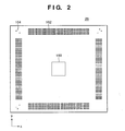
- Fig. 2 shows the structure of the blanking aperture array device 26.
- the blanking aperture array device 26 has an aperture portion 160 having a plurality of openings through which electron beams pass, and the deflection electrode pad 162 and ground electrode pad 164, which serve as connection portions to the blanking aperture array control section 86 shown in Fig. 1.
- the aperture portion 160 is preferably located at the central portion of the blanking aperture array device 26.
- the deflection electrode pad 162 and ground electrode pad 164 supply an electric signal supplied from the blanking aperture array control section 86 through a probe card and pogo-pin array to the deflection electrodes formed in the openings of the aperture portion 160.
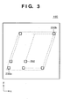
- Fig. 3 shows the structure of the aperture portion 160.
- An X-axis direction is defined in the lateral direction of the aperture portion 160.
- a Y-axis direction is defined in the vertical direction.
- the X-axis indicates the direction in which the wafer stage 46 moves the wafer 44 stepwise during exposure processing.
- the Y-axis indicates the direction in which the wafer stage 46 moves the wafer 44 continuously during exposure processing. More specifically, the Y-axis indicates the scanning/exposure direction of the wafer 44 with respect to the wafer stage 46.
- the X-axis indicates the direction in which the wafer 44 is moved stepwise to exposure unexposed regions of the wafer 44 after the end of scanning/exposure.
- the aperture portion 160 has openings 200 through which the plurality of electron beams should pass.
- the plurality of openings 200 are laid out to expose the entire scanning region.
- the plurality of openings 200 are laid out to cover the whole region between a plurality of openings 200a and 200b which are located at two ends in the X-axis direction.
- the openings 200 close in the X-axis direction are preferably laid out at a predetermined interval.
- the interval between the plurality of openings 200 is preferably defined to be equal to or smaller than the maximum deflection amount of electron beam deflection by the main deflecting section 42.
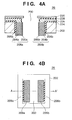
- Figs. 4A and 4B show an example of the detailed structure of the blanking aperture array device 26 according to the first embodiment.
- Fig. 4B is a plan view.
- Fig. 4A is a sectional view taken along a line A - A'.
- the blanking aperture array device 26 comprises a substrate 202 having the openings 200 through which electron beams should pass, deflection electrodes 206a and 206b that oppose each other in each opening 200 to deflect an electron beam, insulating layers 208a and 208b arranged between the substrate 202 and the deflection electrode 206a and between the substrate 202 and the deflection electrode 206b, respectively, an insulating layer 224 formed on the upper surface of the substrate 202, an interconnection layer 226 formed on the upper surface of the insulating layer 224, an insulating layer 228 formed on the upper surface of the interconnection layer 226, and a conductive film 230 formed on the upper surface of the insulating layer 228.
- the insulating layers 208a and 208b electrically insulate the deflection electrodes 206a and 206b from the substrate 202.
- the insulating layer 224 electrically insulates the substrate 202 from the interconnection layer 226.
- the insulating layer 228 electrically insulates the interconnection layer 226 from the conductive film 230.
- the conductive film 230 is electrically connected to the ground electrode pad 164 shown in Fig. 2 and thus grounded.
- the conductive film 230 functions as an anti-charge-up metal layer for the insulating layer 228.
- the deflection electrodes 206a and 206b are electrically connected to the deflection electrode pad 162 shown in Fig. 2 through the interconnection layer 226.
- the deflection electrode 206a has a conductive member 204a and a conductive member 205a formed on the surface of the conductive member 204a.
- the deflection electrode 206b has a conductive member 204b and a conductive member 205b formed on the surface of the conductive member 204b.
- the conductive members 205a and 205b are preferably made of a material that is more difficult to oxidize than the conductive members 204a and 204b.
- the conductive members 204a and 204b are preferably made of a material having a higher plating growth rate than the conductive members 205a and 205b.
- the conductive members 204a and 204b are preferably made of a material whose residual stress after plating growth is smaller than the conductive members 205a and 205b.
- the conductive members 204a and 204b and conductive members 205a and 205b are preferably made of materials having high ionization tendency.
- the conductive members 204a and 204b are made of Cu while the conductive members 205a and 205b are made of Au.
- the conductive members 204a and 204b may be made of a copper alloy containing a trace quantity of Be in Cu.
- the conductive members 205a and 205b may be made of a gold alloy containing a trace quantity of Ag or Pt in Au.
- the substrate 202 is, e.g., a silicon substrate.
- the insulating layers 208a and 208b are oxide films formed by thermally oxidizing the substrate 202 and, for example, silicon oxide films formed by thermally oxidizing a silicon substrate.
- the conductive members 205a and 205b which are difficult to oxidize are formed as the peripheral portions of the deflection electrodes 206a and 206b.
- the deflection electrodes 206a and 206b are bonded to the insulating layers 208a and 208b through the conductive members 204a and 204b with small residual stress. For this reason, degradation of the deflection electrodes 206a and 206b due to oxidization can be prevented while maintaining the bonding strength.
- the blanking aperture array device 26 with a long service life can be provided.
- Fig. 5 shows another example of the detailed structure of the blanking aperture array device 26 according to the first embodiment.
- the structure of the blanking aperture array device 26 shown in Fig. 5 is the same as in Fig, 4 except the following description.
- the deflection electrode 206a also has a conductive member 205c formed on the surface of the conductive member 205a.
- the deflection electrode 206b also has a conductive member 205d formed on the surface of the conductive member 205b.
- the conductive members 205c and 205d are preferably made of a material that is more difficult to oxidize than the conductive members 205a and 205b.
- the conductive members 205c and 205d are preferably made of a material having a lower plating growth rate than the conductive members 205a and 205b.
- the conductive members 205c and 205d are preferably made of a material whose residual stress after plating growth is larger than the conductive members 205a and 205b.
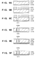
- Figs. 6A to 60 show a method of manufacturing the blanking aperture array device 26.
- the substrate 202 is prepared. Silicon nitride films 210a and 210b are formed on the upper and lower surfaces of the substrate 202, respectively. The silicon nitride films 210a and 210b may be formed either simultaneously or separately.
- the substrate 202 is a silicon wafer having, e.g., a diameter of 6 inches and a thickness of 200 ⁇ m.
- Each of the silicon nitride films 210a and 210b has a thickness of, e.g., 1 ⁇ m.
- a resist 212 is applied to the upper surface of the silicon nitride film 210a. Exposure and development are performed, and the resist 212 is removed from regions where the conductive members 204a and 204b are to be formed. The silicon nitride film 210a in the regions where the conductive members 204a and 204b are to be formed is removed by etching such as reactive ion etching (RIE) using the resist 212 as an etching mask.
- RIE reactive ion etching
- the substrate 202 at the portions where the conductive members 204a and 204b are to be formed is removed by etching such as inductively coupled plasma etching (ICP-RIE) using both or one of the resist 212 and silicon nitride film 210a as an etching mask, thereby forming a plurality of openings 214a and 214b.
- ICP-RIE inductively coupled plasma etching
- the silicon nitride film 210b serves as an etching stopper layer in etching the substrate 202.
- the resist 212 is removed.
- the insulating layers 208a and 208b are formed on the inner walls of the plurality of openings 214a and 214b formed in the substrate 202.
- the insulating layers 208a and 208b are formed by, e.g., thermally oxidizing the inner walls of the plurality of openings 214a and 214b. More specifically, of the inner walls of the plurality of openings 214a and 214b formed in the substrate 202 as a silicon substrate, silicon exposed surfaces except portions covered with the silicon nitride films 210a and 210b are selectively thermally oxidized, thereby forming the insulating layers 208a and 208b as silicon oxide films.
- a conductive film 216 is formed on the silicon nitride film 210b.
- An insulating layer 218 is formed on the conductive film 216. More specifically, a 50-nm thick Cr film, a 200-nm thick Au film, and a 50-nm thick Cr film are formed in this order by e.g. EB deposition to form the conductive film 216 having a multilayered structure of Cr/Au/Cr. When the multilayered structure of Cr/Au/Cr is formed as the conductive film 216, the adhesion between the silicon nitride film 210b and the conductive film 216 can be increased.
- the conductive film 216 may be, e.g., an Au film having a single-layered structure.
- the insulating layer 218 made of a silicon oxide film is formed on the conductive film 216 by e.g. plasma chemical vapor deposition (CVD).
- the silicon nitride film 210b formed in Fig. 6A is used to electrically insulate the substrate 202 from the conductive film 216.
- the silicon nitride film 210a and the portions of the silicon nitride film 210b, which are exposed to the plurality of openings 214a and 214b, are selectively removed by, e.g., RIE.
- the silicon nitride film 210b is etched until the conductive film 216 is exposed to the openings 214a and 214b.
- the Cr film of the conductive film 216 is etched until the Au film is exposed.
- the silicon nitride film 210a and the portions of the silicon nitride film 210b, which are exposed to the plurality of openings 214a and 214b may be removed by wet etching using hot phosphoric acid. After that, the Cr film of the conductive film 216 may be removed by etching in the same way.
- the conductive members 204a and 204b are formed by selectively executing electrolytic plating in the plurality of openings 214a and 214b by using the Au film of the conductive film 216 as a plating electrode (seed layer).
- the conductive members 204a and 204b are made of, e.g., Cu.
- the conductive members 204a and 204b formed outside the openings 214a and 214b are removed by, e.g., chemical mechanical polishing (CMP).
- CMP chemical mechanical polishing
- the conductive members 204a and 204b may be formed inside the Cr films in the plurality of openings 214a and 214b. With this structure, the adhesion between the conductive members 204a and 204b and the insulating layers 208a and 208b can be increased.
- an insulating layer 224 and interconnection layer 226 are formed on the substrate 202. More specifically, the insulating layer 224 as a silicon oxide film having a thickenss of about 1 ⁇ m is formed by e.g. plasma CVD. A resist is applied to the surface of the insulating layer 224. Exposure and development are performed, and the resist above the conductive members 204a and 204b is removed. The insulating layer 224 is removed by etching such as RIE using the resist as an etching mask. After the resist is removed, a Cr film and Au film are deposited on the surface of the insulating layer 224 in this order by sputtering, thereby forming the interconnection layer 226 electrically connected to the conductive members 204a and 204b.
- the insulating layer 224 as a silicon oxide film having a thickenss of about 1 ⁇ m is formed by e.g. plasma CVD.
- a resist is applied to the surface of the insulating layer 224. Exposure and
- an interconnection pattern is formed on the interconnection layer 226. More specifically, a resist is applied to the surface of the interconnection layer 226. Exposure and development are performed, and the resist is removed from a region where no interconnection is to be formed. The interconnection layer 226 is removed by etching such as RIE using the resist as an etching mask, thereby forming the interconnection pattern. Then, the resist is removed.
- an insulating layer 228 and conductive film 230 are formed on the insulating layer 224 and interconnection layer 226. More specifically, the insulating layer 228 as a silicon oxide film having a thickness of about 1 ⁇ m is formed by e.g. plasma CVD. A Cr film and Au film are deposited on the surface of the insulating layer 228 in this order by sputtering to form the conductive film 230.
- a resist 232 is applied to the surface of the conductive film 230. Exposure and development are performed, and the resist 232 is removed from a region where the opening 200 through which an electron beam should pass is to be formed. Using the resist 232 as an etching mask, the conductive film 230 is removed by etching such as ion milling, and the insulating layers 224 and 228 are removed by etching such as RIE.
- the substrate 202 is removed by etching such as ICP-RIE using the resist 232 as an etching mask.
- the portions of the insulating layers 208a and 208b, which are exposed to the opening 200, the insulating layer 218, and the conductive film 216 are removed by etching. More specifically, while leaving the resist 232, the insulating layers 208a and 208b as silicon oxide films on the sidewall of the opening 200 are removed by wet etching using a solution mixture of, e.g., HF and NH 4 F. Simultaneously, the insulating layer 218 is also removed by wet etching.
- the Cr film of the conductive film 216 is removed by wet etching using a solution mixture of, e.g., cerium ammonium nitrate (IV), perchloric acid, and water.
- the Au film of the conductive film 216 is removed by wet etching using a solution mixture of, e.g., potassium iodide, iodine, and water.
- the silicon nitride film 210b is removed by etching. More specifically, the silicon nitride film 210b is removed by wet etching using, e.g., hot phosphoric acid to make the opening 200 through.
- the conductive members 205a and 205b are formed on the surfaces of the conductive members 204a and 204b.
- power is supplied from the interconnection layer 226 to the conductive members 204a and 204b by using the interconnection layer 226 as a plating electrode so that the conductive members 205a and 205b are formed on the surfaces of the conductive members 204a and 204b by electrolytic plating.
- the conductive members 205a and 205b are made of Au.
- the surfaces of the conductive members 204a and 204b may be subjected to activation processing, and the conductive members 205a and 205b may be formed on the surfaces of the conductive members 204a and 204b by electroless plating such as chemical plating or displacement plating. More specifically, the surfaces of the conductive members 204a and 204b made of Cu are subjected to activation processing by acid treatment using an acid except hydrofluoric acid and degreasing cleaning, thereby activating (ionizing) only the surfaces of the conductive members 204a and 204b. Then, using a plating solution containing Au, Au is immersion plating on the surfaces of the conductive members 204a and 204b having high ionization tendency, thereby forming the conductive members 205a and 205b.
- electroless plating such as chemical plating or displacement plating. More specifically, the surfaces of the conductive members 204a and 204b made of Cu are subjected to activation processing by acid treatment using an acid except hydrofluoric
- the same procedures as in formation of the conductive members 205a and 205b are used.
- the lower surface of the substrate 202 is exposed.
- a conductive film may be formed on the lower surface of the substrate 202 to prevent the substrate 202 from being charged up.
- the blanking aperture array device 26 is completed by the manufacturing method shown in Figs. 6A to 60.
- the time required for manufacturing the blanking aperture array device 26 can be shortened because most portions of the deflection electrodes 206a and 206b are formed by the conductive members 204a and 204b having a high plating growth rate.
- the peripheral portions of the deflection electrodes 206a and 206b are formed from the conductive members 205a and 205b which are difficult to oxidize. For this reason, degradation of the deflection electrodes 206a and 206b due to oxidization can be prevented.
- the reliability of electron beam deflection by the blanking aperture array device 26 can be increased.
- the service life of the blanking aperture array device 26 can be prolonged.
- Fig. 7 shows the detailed structure of the blanking aperture array device 26 according to the second embodiment.
- Fig. 7 is a plan view of the blanking aperture array device 26 viewed from the lower surface.
- the blanking aperture array device 26 comprises a substrate 1202 having an opening 200 through which an electron beam should pass, deflection electrodes 1204a and 1204b that oppose each other in the opening 200 to deflect an electron beam, conductive layers 1206a and 1206b which are formed almost perpendicularly to the direction from the deflection electrode 1204a to the deflection electrode 1204b while opposing each other in the opening 200, and insulating layers 1208a and 1208b formed between the substrate 1202 and the deflection electrode 1204a and between the substrate 1202 and the deflection electrode 1204b, respectively.
- the conductive layers 1206a and 1206b are electrically connected to a ground electrode pad 164 shown in Fig. 2 and thus grounded.
- the conductive layers 1206a and 1206b may be connected to the ground electrode pad 164 either directly or via the substrate 1202.
- the conductive layers 1206a and 1206b are preferably made of a material having a high conductivity than the substrate 1202.
- the conductive layers 1206a and 1206b are preferably formed by metal plating.
- the substrate 1202 is, e.g., a silicon substrate.
- the conductive layers 1206a and 1206b are made of, e.g., a material containing Au or Cu as a principal component.
- the insulating layers 1208a and 1208b are oxide films formed by thermally oxidizing the substrate 1202 and, for example, silicon oxide films formed by thermally oxidizing a silicon substrate.
- the length of each of the insulating layers 1208a and 1208b is preferably smaller than the length of each of the deflection electrodes 1204a and 1204b. That is, the insulating layers 1208a and 1208b are shielded from the path of an electron beam by the deflection electrodes 1204a and 1204b. Hence, the insulating layers 1208a and 1208b can be prevented from being charged up.
- the interval between the deflection electrode 1204a and the deflection electrode 1204b is preferably smaller than the interval between the conductive layer 1206a and the conductive layer 1206b.
- the conductive layers 1206a and 1206b may be thinner than the deflection electrodes 1204a and 1204b. More specifically, the deflection electrodes 1204a and 1204b are formed at an interval of several ten ⁇ m. When the interval between the deflection electrode 1204a and the deflection electrode 1204b is small, the electron beam can be accurately deflected. In addition, the voltage applied to the deflection electrodes 1204a and 1204b can be made low.
- the conductive layers 1206a and 1206b are formed on the inner wall of the opening 200, native oxidation of the substrate 1202 can be prevented. Since any native oxide film such as a silicon oxide film that affects the electron beam upon being charged up is not formed on the inner surface of the opening 200, the electron beam can be accurately deflfected.
- Fig. 8 shows a modification of the detailed structure of the blanking aperture array device 26 according to the second embodiment.
- Fig. 8 is a plan view of the blanking aperture array device 26 viewed from the lower surface.
- the same reference numerals as in the blanking aperture array device 26 (Fig. 7) according to the second embodiment denote the same constituent elements in Fig. 8, and a description thereof will be simplified or omitted. Different portions will be described in detail.
- the conductive layers 1206a and 1206b are formed from a position adjacent to the insulating layer 1208a to a position adjacent to the insulating layer 1208b. More specifically, the conductive layers 1206a and 1206b are formed on the inner wall of the opening 200 from a surface on which the deflection electrode 1204a is formed to a surface on which the deflection electrode 1204b is formed. The conductive layers 1206a and 1206b are also formed from the upper end to the lower end of the opening 200 not to make the substrate 1202 expose into the opening 200. In this case, the conductive layers 1206a and 1206b and the deflection electrodes 1204a and 1204b are formed not to come into contact with each other.
- each of the deflection electrodes 1204a and 1204b the surface that opposes the other deflection electrode, i.e., the area of the surface that opposes the electron beam is preferably larger than the area of the surface that opposes the substrate 202, i.e., the area of the surface that is in contact with a corresponding one of the insulating layers 1208a and 1208b.
- each of the deflection electrodes 1204a and 1204b has a trapezoidal columnar shape that is tapered along a direction from the center of the opening 200, i.e., the position at which the electron beam should pass, to the inner wall of the opening 200.
- the width of the surface of each of the deflection electrodes 1204a and 1204b, which opposes the substrate 1202 may be equal to or more than the width of each of the insulating layers 1208a and 1208b.
- the conductive layers 1206a and 1206b are formed to cover the inner wall of the opening 200. For this reason, the influence of the charged-up substrate 1202 on the electron beam can be greatly reduced. Accordingly, the electron beam can be accurately deflected.
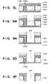
- Figs. 9A to 9P show a method of manufacturing the blanking aperture array device 26 according to the second embodiment shown in Fig. 7 or its modification shown in Fig. 8.
- Figs. 9A to 9P are sectional views of the blanking aperture array device 26 taken along a line A - A' in Fig. 7 or 8.
- the substrate 1202 is prepared. Silicon nitride films 1210a and 1210b are formed on the upper and lower surfaces of the substrate 1202, respectively.
- the silicon nitride films 1210a and 1210b may be formed either simultaneously or separately.
- the substrate 1202 is a silicon wafer having, e.g., a diameter of 6 inches and a thickness of 200 ⁇ m.
- Each of the silicon nitride films 1210a and 1210b has a thickness of, e.g., 1 ⁇ m.
- a resist 1212 is applied to the upper surface of the silicon nitride film 1210a. Exposure and development are performed, and the resist 1212 is removed from regions where the deflection electrodes 1204a and 1204b are to be formed.
- the silicon nitride film 1210a in the regions where the deflection electrodes 1204a and 1204b are to be formed is removed by etching such as reactive ion etching (RIE) using the resist 1212 as an etching mask.
- RIE reactive ion etching
- the substrate 1202 at the portions where the deflection electrodes 1204a and 1204b are to be formed is removed by etching such as inductively coupled plasma etching (ICP-RIE) using both or one of the resist 1212 and silicon nitride film 1210a as an etching mask, thereby forming a plurality of openings 1214.
- ICP-RIE inductively coupled plasma etching
- the silicon nitride film 1210b serves as an etching stopper layer in etching the substrate 1202.
- the resist 1212 is removed.
- the insulating layers 1208a and 1208b are formed on the inner walls of the plurality of openings 1214 formed in the substrate 1202.
- the insulating layers 1208a and 1208b are formed by, e.g., thermally oxidizing the inner walls of the plurality of openings 1214. More specifically, of the inner walls of the plurality of openings 1214 formed in the substrate 1202 as a silicon substrate, silicon exposed surfaces except portions covered with the silicon nitride films 1210a and 1210b are selectively thermally oxidized, thereby forming the insulating layers 1208a and 1208b as silicon oxide films.
- a conductive film 1216 is formed on the silicon nitride film 1210b.
- An insulating layer 1218 is formed on the conductive film 1216. More specifically, a 50-nm thick Cr film, a 200-nm thick Au film, and a 50-nm thick Cr film are formed in this order by e.g. EB deposition to form the conductive film 1216 having a multilayered structure of Cr/Au/Cr. When the multilayered structure of Cr/Au/Cr is formed as the conductive film 1216, the adhesion between the silicon nitride film 1210b and the conductive film 1216 can be increased.
- the conductive film 1216 may be, e.g., an Au film having a single-layered structure.
- the insulating layer 1218 made of a silicon oxide film is formed on the conductive film 1216 by e.g. plasma chemical vapor deposition (CVD).
- the silicon nitride film 1210b formed in Fig. 9A is used to electrically insulate the substrate 1202 from the conductive film 1216.
- the silicon nitride film 1210a and the portions of the silicon nitride film 1210b, which are exposed to the plurality of openings 1214, are selectively removed by, e.g., RIE.
- the silicon nitride film 1210b is etched until the conductive film 1216 is exposed to the plurality of openings 1214.
- the Cr film of the conductive film 1216 is etched until the Au film is exposed.
- the silicon nitride film 1210a and the portions of the silicon nitride film 1210b, which are exposed to the plurality of openings 1214 may be removed by wet etching using hot phosphoric acid. After that, the Cr film of the conductive film 1216 may be removed by etching in the same way.
- the deflection electrodes 1204a and 1204b are formed by selectively executing electrolytic plating in the plurality of openings 1214 by using the Au film of the conductive film 1216 as a plating electrode (seed layer) and filling the openings 1214 with a conductive material.
- the deflection electrodes 1204a and 1204b are made of, e.g., Cu or Au.
- the conductive material of the deflection electrodes 1204a and 1204b which is formed outside the openings 1214, is removed by, e.g., chemical mechanical polishing (CMP).
- CMP chemical mechanical polishing
- the interiors of the Cr films of the plurality of openings 1214 may be filled with the conductive material to form the deflection electrodes 1204a and 1204b.
- the adhesion between the deflection electrodes 1204a and 1204b and the insulating layers 1208a and 1208b can be increased.
- a resist 1220 is applied to the upper surface of the substrate 1202. Exposure and development are performed, and the resist 1220 is removed from regions where the conductive layers 1206a and 1206b are to be formed.
- the substrate 1202 at portions where the conductive layers 1206a and 1206b are to be formed is selectively removed by etching such as RIE using the resist 1220 as an etching mask, thereby forming openings 1222. Portions of the silicon nitride film 1210b, which are exposed to the openings 1222, are selectively removed by, e.g., RIE.
- the Cr film of the conductive film 1216 is etched until the Au film is exposed.
- the portions of the silicon nitride film 1210b, which are exposed to the openings 1222, and the Cr film of the conductive film 1216 may be removed by wet etching using hot phosphoric acid.
- the conductive layers 1206a and 1206b are formed by selectively executing electrolytic plating in the openings 1222 by using the Au film of the conductive film 1216 as a plating electrode (seed layer) and filling the openings 1222 with a conductive material.
- the conductive layers 1206a and 1206b are made of, e.g., Cu. After the conductive layers 1206a and 1206b are formed, the resist 1220 is removed, and an unnecessary conductive material is removed by, e.g., CMP.
- the interiors of the Cr films of the openings 1222 may be filled with the conductive material to form the conductive layers 1206a and 1206b.
- the adhesion between the conductive layers 1206a and 1206b and the substrate 1202 can be increased.
- an insulating layer 1224 and interconnection layer 1226 are formed on the substrate 1202. More specifically, the insulating layer 1224 as a silicon oxide film having a thickness of about 1 ⁇ m is formed by e.g. plasma CVD. A resist is applied to the surface of the insulating layer 1224. Exposure and development are performed, and the resist above the deflection electrodes 1204a and 1204b is removed. The insulating layer 1224 is removed by etching such as RIE using the resist as an etching mask. After the resist is removed, a Cr film and Au film are deposited on the surface of the insulating layer 1224 in this order by sputtering, thereby forming the interconnection layer 1226.
- the insulating layer 1224 as a silicon oxide film having a thickness of about 1 ⁇ m is formed by e.g. plasma CVD.
- a resist is applied to the surface of the insulating layer 1224. Exposure and development are performed, and the resist above the deflection electrodes 1204a and 1204
- an interconnection pattern is formed on the interconnection layer 1226. More specifically, a resist is applied to the surface of the interconnection layer 1226. Exposure and development are performed, and the resist is removed from a region where no interconnection is to be formed. The interconnection layer 1226 is removed by etching such as RIE using the resist as an etching mask, thereby forming the interconnection pattern. Then, the resist is removed.
- an insulating layer 1228 and conductive film 1230 are formed on the insulating layer 1224 and interconnection layer 1226. More specifically, the insulating layer 1228 as a silicon oxide film having a thickness of about 1 ⁇ m is formed by e.g. plasma CVD. A Cr film and Au film are deposited on the surface of the insulating layer 1228 in this order by sputtering to form the conductive film 1230. The conductive film 1230 is grounded and thus functions as an anti-charge-up metal layer for the insulating layer 1228.
- a resist 1232 is applied to the surface of the conductive film 1230. Exposure and development are performed, and the resist 1232 is removed from a region where the opening 200 through which an electron beam should pass is to be formed. Using the resist 1232 as an etching mask, the conductive film 1230 is removed by etching such as ion milling, and the insulating layers 1224 and 1228 are removed by etching such as RIE.
- the substrate 1202 is removed by etching such as ICP-RIE using the resist 1232 as an etching mask. At this time, the opening 200 having an I shape when viewed from the upper side is formed.
- the portions of the insulating layers 1208a and 1208b, which are exposed to the opening 200, the insulating layer 1218, and the conductive film 1216 are removed by etching. More specifically, while leaving the resist 1232, the insulating layers 1208a and 1208b as silicon oxide films on the sidewall of the opening 200 are removed by wet etching using a solution mixture of, e.g., HF and NH 4 F. Simultaneously, the insulating layer 1218 is also removed by wet etching.
- the Cr film of the conductive film 1216 is removed by wet etching using a solution mixture of, e.g., cerium ammonium nitrate (IV), perchloric acid, and water.
- the Au film of the conductive film 1216 is removed by wet etching using a solution mixture of, e.g., potassium iodide, iodine, and water.
- the silicon nitride film 1210b is removed by etching. More specifically, the silicon nitride film 1210b is removed by wet etching using, e.g., hot phosphoric acid to make the opening 200 through. In this embodiment, the lower surface of the substrate 1202 is exposed. However, a conductive film may be formed on the lower surface of the substrate 1202 to prevent the substrate 1202 from being charged up. In the above way, the blanking aperture array device 26 is completed by the manufacturing method shown in Figs. 9A to 9P.
- the conductive layers 1206a and 1206b are in contact with the substrate 1202, the conductive layers 1206a and 1206b can be grounded through the substrate 1202. Hence, no interconnection need be formed to ground the conductive layers 1206a and 1206b, and the interconnection density can be reduced.
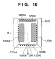
- Fig. 10 shows the detailed structure of a blanking aperture array device 26 according to the third embodiment.
- Fig. 10 is a plan view of the blanking aperture array device 26 viewed from the lower surface.
- the same reference numerals as in the blanking aperture array devices 26 according to the second embodiment and its modification denote the same constituent elements in the third embodiment, and a description thereof will be simplified or omitted. Different portions will be described in detail.
- the blanking aperture array device 26 further comprises insulating layers 1208c and 1208d formed between a substrate 1202 and a conductive layer 1206a and between the substrate 1202 and a conductive layer 1206b. Insulating layers 1208a and 1208b and the insulating layers 1208c and 1208d can be made of the same material and have almost the same thickness.
- the insulating layers 1208c and 1208d are oxide films formed by thermally oxidizing the substrate 1202 and, for example, silicon oxide films formed by thermally oxidizing a silicon substrate.
- the width of each of the insulating layers 1208c and 1208d is preferably smaller than the width of each of the conductive layers 1206a and 1206b. That is, the insulating layers 1208c and 1208d are shielded from the path of an electron beam by the conductive layers 1206a and 1206b. Hence, the insulating layers 1208c and 1208d can be prevented from being charged up.
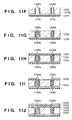
- Figs. 11A to 11N show a method of manufacturing the blanking aperture array device 26 according to the third embodiment.
- Figs. 11A to 11N are sectional views of the blanking aperture array device 26 taken along a line B - B' in Fig. 10.
- the substrate 1202 is prepared. Silicon nitride films 1210a and 1210b are formed on the upper and lower surfaces of the substrate 1202, respectively.
- the silicon nitride films 1210a and 1210b may be formed either simultaneously or separately.
- the substrate 1202 is a silicon wafer having, e.g., a diameter of 6 inches and a thickness of 200 ⁇ m.
- Each of the silicon nitride films 1210a and 1210b has a thickness of, e.g., 1 ⁇ m.
- a resist 1212 is applied to the upper surface of the silicon nitride film 1210a. Exposure and development are performed, and the resist 1212 is removed from regions where the deflection electrodes 1204a and 1204b and conductive layers 1206a and 1206b are to be formed. The silicon nitride film 1210a in the regions where the deflection electrodes 1204a and 1204b and conductive layers 1206a and 1206b are to be formed is removed by etching such as RIE using the resist 1212 as an etching mask.
- the substrate 1202 at the portions where the deflection electrodes 1204a and 1204b and conductive layers 1206a and 1206b are to be formed is removed by etching such as ICP-RIE using both or one of the resist 1212 and silicon nitride film 1210b as an etching mask, thereby forming a plurality of openings 1214 and 1222.
- the silicon nitride film 1210b serves as an etching stopper layer in etching the substrate 1202.
- the resist 1212 is removed.
- the insulating layers 1208a, 1208b, 1208c, and 1208d are formed on the inner walls of the plurality of openings 1214 and 1222 formed in the substrate 1202.
- the insulating layers 1208a, 1208b, 1208c, and 1208d are formed by, e.g., thermally oxidizing the inner walls of the plurality of openings 1214 and 1222.
- silicon exposed surfaces except portions covered with the silicon nitride films 1210a and 1210b are selectively thermally oxidized, thereby forming the insulating layers 1208a, 1208b, 1208c, and 1208d as silicon oxide films.
- a conductive film 1216 is formed on the silicon nitride film 1210b.
- An insulating layer 1218 is formed on the conductive film 1216. More specifically, a 50-nm thick Cr film, a 200-nm thick Au film, and a 50-nm thick Cr film are formed in this order by e.g. EB deposition to form the conductive film 1216 having a multilayered structure of Cr/Au/Cr. When the multilayered structure of Cr/Au/Cr is formed as the conductive film 1216, the adhesion between the silicon nitride film 1210b and the conductive film 1216 can be increased.
- the conductive film 1216 may be, e.g., an Au film having a single-layered structure.
- the insulating layer 1218 made of a silicon oxide film is formed on the conductive film 1216 by e.g. plasma CVD.
- the silicon nitride film 1210b formed in Fig. 11A is used to electrically insulate the substrate 1202 from the conductive film 1216.
- the silicon nitride film 1210a and the portions of the silicon nitride film 1210b, which are exposed to the plurality of openings 1214 and 1222, are selectively removed by, e.g., RIE.
- the silicon nitride film 1210b is etched until the conductive film 1216 is exposed to the plurality of openings 1214 and 1222.
- the Cr film of the conductive film 1216 is etched until the Au film is exposed.
- the silicon nitride film 1210a and the portions of the silicon nitride film 1210b, which are exposed to the plurality of openings 1214 and 1222 may be removed by wet etching using hot phosphoric acid. After that, the Cr film of the conductive film 1216 may be removed by etching in the same way.
- the deflection electrodes 1204a and 1204b and conductive layers 1206a and 1206b are formed by selectively executing electrolytic plating in the plurality of openings 1214 and 1222 by using the Au film of the conductive film 1216 as a plating electrode (seed layer) and filling the openings 1214 and 1222 with a conductive material.
- the deflection electrodes 1204a and 1204b and conductive layers 1206a and 1206b are made of, e.g., Cu or Au.
- an unnecessary conductive material is removed by, e.g., CMP.
- the interiors of the Cr films of the plurality of openings 1214 and 1222 may be filled with the conductive material to form the deflection electrodes 1204a and 1204b and conductive layers 1206a and 1206b.
- the adhesion between the deflection electrodes 1204a and 1204b and conductive layers 1206a and 1206b and the insulating layers 1208a, 1208b, 1208c, and 1208d can be increased.
- an insulating layer 1224 and interconnection layer 1226 are formed on the substrate 1202. More specifically, the insulating layer 1224 as a silicon oxide film having a thickness of about 1 ⁇ m is formed by e.g. plasma CVD. A resist is applied to the surface of the insulating layer 1224. Exposure and development are performed, and the resist above the deflection electrodes 1204a and 1204b and conductive layers 1206a and 1206b is removed. The insulating layer 1224 is removed by etching such as RIE using the resist as an etching mask. After the resist is removed, a Cr film and Au film are deposited on the surface of the insulating layer 1224 in this order by sputtering, thereby forming the interconnection layer 1226.
- RIE reactive etching
- an interconnection pattern is formed on the interconnection layer 1226. More specifically, a resist is applied to the surface of the interconnection layer 1226. Exposure and development are performed, and the resist is removed from a region where no interconnection is to be formed. The interconnection layer 1226 is removed by etching such as RIE using the resist as an etching mask, thereby forming the interconnection pattern. Then, the resist is removed.
- an insulating layer 1228 and conductive film 1230 are formed on the insulating layer 1224 and interconnection layer 1226. More specifically, the insulating layer 1228 as a silicon oxide film having a thickness of about 1 ⁇ m is formed by e.g. plasma CVD. A Cr film and Au film are deposited on the surface of the insulating layer 1228 in this order by sputtering to form the conductive film 1230. The conductive film 1230 is grounded and thus functions as an anti-charge-up metal layer for the insulating layer 1228.
- a resist 1232 is applied to the surface of the conductive film 1230. Exposure and development are performed, and the resist 1232 is removed from a region where an opening 200 through which an electron beam should pass. Using the resist 1232 as an etching mask, the conductive film 1230 is removed by etching such as ion milling, and the insulating layers 1224 and 1228 are removed by etching such as RIE.
- the substrate 1202 is removed by etching such as ICP-RIE using the resist 1232 as an etching mask. At this time, the opening 200 having an I shape when viewed from the upper side is formed.
- the portions of the insulating layers 1208a, 1208b, 1208c, and 1208d, which are exposed to the opening 200, the insulating layer 1218, and the conductive film 1216 are removed by etching. More specifically, while leaving the resist 1232, the insulating layers 1208a, 1208b, 1208c, and 1208d as silicon oxide films on the sidewall of the opening 200 are removed by wet etching using a solution mixture of, e.g., HF and NH 4 F. Simultaneously, the insulating layer 1218 is also removed by wet etching.
- the Cr film of the conductive film 1216 is removed by wet etching using a solution mixture of, e.g., cerium ammonium nitrate (IV), perchloric acid, and water.
- the Au film of the conductive film 1216 is removed by wet etching using a solution mixture of, e.g., potassium iodide, iodine, and water.
- the silicon nitride film 1210b is removed by etching. More specifically, the silicon nitride film 1210b is removed by wet etching using, e.g., hot phosphoric acid to make the opening 200 through. In this embodiment, the lower surface of the substrate 1202 is exposed. However, a conductive film may be formed on the lower surface of the substrate 1202 to prevent the substrate 1202 from being charged up. In the above way, the blanking aperture array device 26 is completed by the manufacturing method shown in Figs. 11A to 11N.
- the deflection electrodes 1204a and 1204b and conductive layers 1206a and 1206b have the same structure, the deflection electrodes 1204a and 1204b and conductive layers 1206a and 1206b can be simultaneously formed. For this reason, the number of steps in manufacturing the blanking aperture array device 26 can be decreased.
- the fourth embodiment will be described next.
- the arrangement of an electron beam exposure apparatus 100, the structure of a blanking aperture array device 26, and the structure of an aperture portion 160 are the same as in the first embodiment (Figs. 1 to 3).
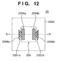
- Fig. 12 shows the detailed structure of the blanking aperture array device 26 according to the fourth embodiment.
- the blanking aperture array device 26 comprises: a substrate 2202 having a through hole 200 through which an electron beam should pass and two groove portions 2201a and 2201b formed in two side surfaces opposite to each other inside the through hole 200; two deflection electrodes 2204a and 2204b which oppose each other in the through hole 200 so as to deflect an electron beam and are at least partially buried in the two groove portions 2201a and 2201b; and insulating layers 2208a and 2208b formed between the substrate 2202 and the buried portion of the deflection electrode 2204a and between the substrate 2202 and the buried portion of the deflection electrode 2204b in the groove portions 2201a and 2201b.
- the groove portions 2201a and 2201b have shapes to lock the buried portions of the deflection electrodes 2204a and 2204b in the groove portions 2201a and 2201b to prevent the deflection electrodes 2204a and 2204b from separating from the substrate 2202. More specifically, in the section almost perpendicular to the electron beam irradiation direction, i.e., the direction of thickness of the substrate 2202, preferably, the maximum width of the buried portion of the deflection electrode 2204a in the groove portion 2201a is larger than the width of the upper surface of the groove portion 2201a, and the maximum width of the buried portion of the deflection electrode 2204b in the groove portion 2201b is larger than the width of the upper surface of the groove portion 2201b.
- each of the deflection electrodes 2204a and 2204b in the through hole 200 is preferably larger than the width of the upper surface of a corresponding one of the groove portions 2201a and 2201b.
- the upper surface of each of the groove portions 2201a and 2201b indicates the interface (contact surface) between the through hole 200 and each of the groove portions 2201a and 2201b.
- the buried portions of the deflection electrodes 2204a and 2204b in the groove portions 2201a and 2201b and the groove portions 2201a and 2201b have trapezoidal columnar shapes.
- the deflection electrodes 2204a and 2204b are held while engaging with the groove portions 2201a and 2201b, respectively.
- the groove portions 2201a and 2201b may be formed partially in the direction of thickness of the substrate 2202 or from the upper surface to the lower surface.
- the deflection electrodes 2204a and 2204b may be formed partially in the direction of thickness of the substrate 2202 or from the upper surface to the lower surface.
- the buried portions of the deflection electrodes 2204a and 2204b in the groove portions 2201a and 2201b may be formed partially in the direction of thickness of the substrate 2202 or from the upper surface to the lower surface.
- the substrate 2202 is, e.g., a silicon substrate.
- the insulating layers 2208a and 2208b are oxide films formed by thermally oxidizing the substrate 2202 and, for example, silicon oxide films formed by thermally oxidizing a silicon substrate.
- the insulating layers 2208a and 2208b may be formed only inside the groove portions 2201a and 2201b.
- the insulating layers 2208a and 2208b may be formed to the through hole 200 across the interfaces from the groove portions 2201a and 2201b. That is, the insulating layers 2208a and 2208b may be partially exposed to the through hole 200 from the groove portions 2201a and 2201b.
- the groove portion 2201a and deflection electrode 2204a preferably have similar shapes.
- the groove portion 2201b and deflection electrode 2204b preferably have similar shapes.
- each of the groove portions 2201a and 2201b may have a widest portion between the upper surface and the bottom surface in the section almost perpendicular to the direction of thickness of the substrate 2202.
- Each of the groove portions 2201a and 2201b may have a curved bottom surface.
- the groove portions 2201a and 2201b may extend from the center of the through hole 200 to the deflection electrodes 2204a and 2204b, or temporarily become narrow and then extend.
- Each of the groove portions 2201a and 2201b may be branched into a plurality of parts.
- the plurality of parts may extend from the center of the through hole 200 to the deflection electrodes 2204a and 2204b. More specifically, in the section almost perpendicular to the direction of thickness of the substrate 2202, the groove portions 2201a and 2201b only need to have side surfaces for which normals heading from the groove portions 2201a and 2201b to the deflection electrodes 2204a and 2204b separate from the through hole 200.
- the deflection electrodes 2204a and 2204b are buried in the groove portions 2201a and 2201b. For this reason, the deflection electrodes 2204a and 2204b can be prevented from peeling off from the substrate 2202.
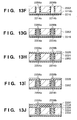
- Figs. 13A to 13N show a method of manufacturing the blanking aperture array device 26.
- Figs. 13A to 13N show the section of the blanking aperture array device 26 taken along a line A - A' in Fig. 12.
- the substrate 2202 is prepared. Silicon nitride films 2210a and 2210b are formed on the upper and lower surfaces of the substrate 2202, respectively.
- the silicon nitride films 2210a and 2210b may be formed either simultaneously or separately.
- the substrate 2202 is a silicon wafer having, e.g., a diameter of 6 inches and a thickness of 200 ⁇ m.
- Each of the silicon nitride films 2210a and 2210b has a thickness of, e.g., 1 ⁇ m.
- a resist 2212 is applied to the upper surface of the silicon nitride film 2210a. Exposure and development are performed, and the resist 2212 is removed from regions where the deflection electrodes 2204a and 2204b are to be formed.
- the silicon nitride film 2210a in the regions where the deflection electrodes 2204a and 2204b are to be formed is removed by etching such as reactive ion etching (RIE) using the resist 2212 as an etching mask.
- RIE reactive ion etching
- the substrate 2202 at the portions where the deflection electrodes 2204a and 2204b are to be formed is removed by etching such as inductively coupled plasma etching (ICP-RIE) using both or one of the resist 2212 and silicon nitride film 2210a as an etching mask, thereby forming a plurality of openings 2214a and 2214b.
- ICP-RIE inductively coupled plasma etching
- the openings 2214a and 2214b include spaces where the groove portions 2201a and 2201b shown in Fig. 12 should be formed.
- Openings where the deflection electrodes 2204a and 2204b should be formed are formed in the substrate 2202 such that the openings have shapes to lock the buried portions of the deflection electrodes 2204a and 2204b in the groove portions 2201a and 2201b so that the groove portions 2201a and 2201b prevent the deflection electrodes 2204a and 2204b from separating from the substrate 2202.
- the openings 2214a and 2214b where the deflection electrodes 2204a and 2204b should be formed are formed such that the maximum width of the buried portion of each of the deflection electrodes 2204a and 2204b in the groove portions 2201a and 2201b becomes larger than the width of the upper surface of a corresponding one of the groove portions 2201a and 2201b.
- the silicon nitride film 2210b serves as an etching stopper layer in etching the substrate 2202.
- the resist 2212 is removed.
- the insulating layers 2208a and 2208b are formed on the inner walls of the openings 2214a and 2214b formed in the substrate 2202.
- the insulating layers 2208a and 2208b are formed by, e.g., thermally oxidizing the inner walls of the openings 2214a and 2214b. More specifically, of the inner walls of the openings 2214a and 2214b formed in the substrate 2202 as a silicon substrate, silicon exposed surfaces except portions covered with the silicon nitride films 2210a and 2210b are selectively thermally oxidized, thereby forming the insulating layers 2208a and 2208b as silicon oxide films.
- a conductive film 2216 is formed on the silicon nitride film 2210b.
- An insulating layer 2218 is formed on the conductive film 2216. More specifically, a 50-nm thick Cr film, a 20-nm thick Au film, and a 50-nm thick Cr film are formed in this order by e.g. EB deposition to form the conductive film 2216 having a multilayered structure of Cr/Au/Cr. When the multilayered structure of Cr/Au/Cr is formed as the conductive film 2216, the adhesion between the silicon nitride film 2210b and the conductive film 2216 can be increased.
- the conductive film 2216 may be, e.g., an Au film having a single-layered structure.
- the insulating layer 2218 made of a silicon oxide film is formed on the conductive film 2216 by e.g. plasma chemical vapor deposition (CVD).
- the silicon nitride film 2210b formed in Fig. 13A is used to electrically insulate the substrate 2202 from the conductive film 2216.
- the silicon nitride film 2210a and the portions of the silicon nitride film 2210b, which are exposed to the openings 2214a and 2214b, are selectively removed by, e.g., RIE.
- the silicon nitride film 2210b is etched until the conductive film 2216 is exposed to the openings 2214a and 2214b.
- the Cr film of the conductive film 2216 is etched until the Au film is exposed.
- the silicon nitride film 2210a, the portions of the silicon nitride film 2210b, which are exposed to the openings 2214a and 2214b, and the Cr film of the conductive film 2216 may be removed by wet etching using hot phosphoric acid.
- the deflection electrodes 2204a and 2204b are formed inside the insulating layers 2208a and 2208b, respectively, by selectively executing electrolytic plating in the openings 2214a and 2214b by using the Au film of the conductive film 2216 as a plating electrode (seed layer).
- the deflection electrodes 2204a and 2204b are made of, e.g., Cu. After the deflection electrodes 2204a and 2204b are formed, an unnecessary conductive material is removed by, e.g., chemical mechanical polishing (CMP).
- CMP chemical mechanical polishing
- the deflection electrodes 2204a and 2204b may be formed inside the Cr films in the openings 2214a and 2214b. With this structure, the adhesion between the deflection electrodes 2204a and 2204b and the insulating layers 2208a and 2208b can be increased.
- an insulating layer 2224 and interconnection layer 2226 are formed on the substrate 2202. More specifically, the insulating layer 2224 as a silicon oxide film having a thickness of about 1 ⁇ m is formed by e.g. plasma CVD. A resist is applied to the surface of the insulating layer 2224. Exposure and development are performed, and the resist above the deflection electrodes 2204a and 2204b is removed. The insulating layer 2224 is removed by etching such as RIE using the resist as an etching mask.
- a Cr film and Au film are deposited on the surface of the insulating layer 2224 in this order by sputtering, thereby forming the interconnection layer 2226 electrically connected to the deflection electrodes 2204a and 2204b.
- an interconnection pattern is formed on the interconnection layer 2226. More specifically, a resist is applied to the surface of the interconnection layer 2226. Exposure and development are performed, and the resist is removed from a region where no interconnection is to be formed. The interconnection layer 2226 is removed by etching such as RIE using the resist as an etching mask, thereby forming the interconnection pattern. Then, the resist is removed.
- an insulating layer 2228 and conductive film 2230 are formed on the insulating layer 2224 and interconnection layer 2226. More specifically, the insulating layer 2228 as a silicon oxide film having a thickness of about 1 ⁇ m is formed by e.g. plasma CVD. A Cr film and Au film are deposited on the surface of the insulating layer 2228 in this order by sputtering to form the conductive film 2230. The conductive film 2230 is grounded and thus functions as an anti-charge-up metal layer for the insulating layer 2228.
- a resist 2232 is applied to the surface of the conductive film 2230. Exposure and development are performed, and the resist 2232 is removed from a region where the through hole 200 through which an electron beam should pass is to be formed. Using the resist 2232 as an etching mask, the conductive film 2230 is removed by etching such as ion milling, and the insulating layers 2224 and 2228 are removed by etching such as RIE.
- the substrate 2202 is removed by etching such as ICP-RIE using the resist 2232 as an etching mask, thereby forming the through hole 200 through which the electron beam should pass in the substrate 2202.
- parts of the insulating layers 2208a and 2208b, the insulating layer 2218, and the conductive film 2216 are removed by etching. More specifically, while leaving the insulating layers 2208a and 2208b in the groove portions 2201a and 2201b, the insulating layers 2208a and 2208b on the sidewall of the through hole 200 are removed by wet etching using a solution mixture of, e.g., HF and NH 4 F. Simultaneously, the insulating layer 2218 is also removed by wet etching.
- the Cr film of the conductive film 2216 is removed by wet etching using a solution mixture of, e.g., cerium ammonium nitrate (IV), perchloric acid, and water.
- the Au film of the conductive film 2216 is removed by wet etching using a solution mixture of, e.g., potassium iodide, iodine, and water.
- the silicon nitride film 2210b is removed by etching. More specifically, the silicon nitride film 2210b is removed by wet etching using, e.g., hot phosphoric acid to make the through hole 200 through. In this embodiment, the lower surface of the substrate 2202 is exposed. However, a conductive film may be formed on the lower surface of the substrate 2202 to prevent the substrate 2202 from being charged up. In the above way, the blanking aperture array device 26 is completed by the manufacturing method shown in Figs. 13A to 13N.
- the deflection electrodes 2204a and 2204b are buried in the groove portions 2201a and 2201b. Even when the deflection electrodes 2204a and 2204b are formed by plating inside the insulating layers 2208a and 2208b by using a material having a relatively large residual stress after plating growth, the peeling resistance of the deflection electrodes 2204a and 2204b and insulating layers 2208a and 2208b can be increased. Hence, the reliability of electron beam deflection by the blanking aperture array device 26 can be increased. In addition, the service life of the blanking aperture array device 26 can be prolonged.
- a deflector which accurately deflects a charged particle beam and has a long service life, a method of manufacturing the deflector, and a charged particle beam exposure apparatus having the deflector.
Landscapes
- Chemical & Material Sciences (AREA)
- Engineering & Computer Science (AREA)
- Nanotechnology (AREA)
- Analytical Chemistry (AREA)
- Physics & Mathematics (AREA)
- Crystallography & Structural Chemistry (AREA)
- Condensed Matter Physics & Semiconductors (AREA)
- General Physics & Mathematics (AREA)
- Manufacturing & Machinery (AREA)
- Mathematical Physics (AREA)
- Theoretical Computer Science (AREA)
- Electron Beam Exposure (AREA)
Priority Applications (1)
| Application Number | Priority Date | Filing Date | Title |
|---|---|---|---|
| EP12190098.9A EP2555219B1 (de) | 2002-10-03 | 2003-10-01 | Deflektor, Verfahren zur Herstellung des Deflektors und Belichtungsvorrichtung mit geladenem Teilchenstrahl |
Applications Claiming Priority (6)
| Application Number | Priority Date | Filing Date | Title |
|---|---|---|---|
| JP2002291710A JP2004128285A (ja) | 2002-10-03 | 2002-10-03 | 偏向器、偏向器の製造方法、及び荷電粒子線露光装置 |
| JP2002291709A JP4076834B2 (ja) | 2002-10-03 | 2002-10-03 | 偏向器、偏向器の製造方法、及び荷電粒子線露光装置 |
| JP2002291710 | 2002-10-03 | ||
| JP2002291709 | 2002-10-03 | ||
| JP2002313423 | 2002-10-28 | ||
| JP2002313423A JP4071085B2 (ja) | 2002-10-28 | 2002-10-28 | 偏向器、偏向器の製造方法、及び荷電粒子線露光装置 |
Related Child Applications (2)
| Application Number | Title | Priority Date | Filing Date |
|---|---|---|---|
| EP12190098.9A Division EP2555219B1 (de) | 2002-10-03 | 2003-10-01 | Deflektor, Verfahren zur Herstellung des Deflektors und Belichtungsvorrichtung mit geladenem Teilchenstrahl |
| EP12190098.9A Division-Into EP2555219B1 (de) | 2002-10-03 | 2003-10-01 | Deflektor, Verfahren zur Herstellung des Deflektors und Belichtungsvorrichtung mit geladenem Teilchenstrahl |
Publications (3)
| Publication Number | Publication Date |
|---|---|
| EP1406290A2 true EP1406290A2 (de) | 2004-04-07 |
| EP1406290A3 EP1406290A3 (de) | 2011-03-09 |
| EP1406290B1 EP1406290B1 (de) | 2014-08-06 |
Family
ID=31998783
Family Applications (2)
| Application Number | Title | Priority Date | Filing Date |
|---|---|---|---|
| EP03256205.0A Expired - Lifetime EP1406290B1 (de) | 2002-10-03 | 2003-10-01 | Ablenkvorrichtung, Verfahren zu deren Herstellung und Belichtungsgerät für geladene Teilchen |
| EP12190098.9A Expired - Lifetime EP2555219B1 (de) | 2002-10-03 | 2003-10-01 | Deflektor, Verfahren zur Herstellung des Deflektors und Belichtungsvorrichtung mit geladenem Teilchenstrahl |
Family Applications After (1)
| Application Number | Title | Priority Date | Filing Date |
|---|---|---|---|
| EP12190098.9A Expired - Lifetime EP2555219B1 (de) | 2002-10-03 | 2003-10-01 | Deflektor, Verfahren zur Herstellung des Deflektors und Belichtungsvorrichtung mit geladenem Teilchenstrahl |
Country Status (2)
| Country | Link |
|---|---|
| US (2) | US6953938B2 (de) |
| EP (2) | EP1406290B1 (de) |
Cited By (2)
| Publication number | Priority date | Publication date | Assignee | Title |
|---|---|---|---|---|
| EP1355192A3 (de) * | 2002-04-10 | 2010-05-26 | Canon Kabushiki Kaisha | Arraystruktur für ein Ladungsträgerteilchenstrahl-Belichtungsgerät und Herstellungsverfahren |
| EP2214194A1 (de) * | 2009-01-28 | 2010-08-04 | IMS Nanofabrication AG | Verfahren zur Herstellung einer Vorrichtung mit Mehrstrahlen-Ablenkanordnung mit Elektroden |
Families Citing this family (37)
| Publication number | Priority date | Publication date | Assignee | Title |
|---|---|---|---|---|
| EP1463087B1 (de) * | 2003-03-24 | 2010-06-02 | ICT, Integrated Circuit Testing Gesellschaft für Halbleiterprüftechnik Mbh | Ladungsträgerstrahlvorrichtung |
| US7838839B2 (en) * | 2003-12-30 | 2010-11-23 | Commissariat A L'energie Atomique | Hybrid multibeam electronic emission device with controlled divergence |
| JP4657740B2 (ja) * | 2005-01-26 | 2011-03-23 | キヤノン株式会社 | 荷電粒子線光学系用収差測定装置、該収差測定装置を具備する荷電粒子線露光装置及び該装置を用いたデバイス製造方法 |
| JP4805686B2 (ja) * | 2006-02-09 | 2011-11-02 | 株式会社ニューフレアテクノロジー | 電子線描画装置用偏向器及び電子線描画装置 |
| JP2007231324A (ja) * | 2006-02-28 | 2007-09-13 | Canon Inc | マルチ荷電ビーム加工装置 |
| JP5103033B2 (ja) * | 2007-03-02 | 2012-12-19 | 株式会社日立ハイテクノロジーズ | 荷電粒子線応用装置 |
| DE102015202172B4 (de) | 2015-02-06 | 2017-01-19 | Carl Zeiss Microscopy Gmbh | Teilchenstrahlsystem und Verfahren zur teilchenoptischen Untersuchung eines Objekts |
| DE102018202428B3 (de) | 2018-02-16 | 2019-05-09 | Carl Zeiss Microscopy Gmbh | Vielstrahl-Teilchenmikroskop |
| DE102018202421B3 (de) | 2018-02-16 | 2019-07-11 | Carl Zeiss Microscopy Gmbh | Vielstrahl-Teilchenstrahlsystem |
| CN112055886A (zh) | 2018-02-27 | 2020-12-08 | 卡尔蔡司MultiSEM有限责任公司 | 带电粒子多束系统及方法 |
| US10811215B2 (en) | 2018-05-21 | 2020-10-20 | Carl Zeiss Multisem Gmbh | Charged particle beam system |
| DE102018115012A1 (de) | 2018-06-21 | 2019-12-24 | Carl Zeiss Microscopy Gmbh | Teilchenstrahlsystem |
| DE102018007455B4 (de) | 2018-09-21 | 2020-07-09 | Carl Zeiss Multisem Gmbh | Verfahren zum Detektorabgleich bei der Abbildung von Objekten mittels eines Mehrstrahl-Teilchenmikroskops, System sowie Computerprogrammprodukt |
| DE102018007652B4 (de) | 2018-09-27 | 2021-03-25 | Carl Zeiss Multisem Gmbh | Teilchenstrahl-System sowie Verfahren zur Stromregulierung von Einzel-Teilchenstrahlen |
| DE102018124044B3 (de) | 2018-09-28 | 2020-02-06 | Carl Zeiss Microscopy Gmbh | Verfahren zum Betreiben eines Vielstrahl-Teilchenstrahlmikroskops und Vielstrahl-Teilchenstrahlsystem |
| DE102018124219A1 (de) | 2018-10-01 | 2020-04-02 | Carl Zeiss Microscopy Gmbh | Vielstrahl-Teilchenstrahlsystem und Verfahren zum Betreiben eines solchen |
| US11145485B2 (en) * | 2018-12-26 | 2021-10-12 | Nuflare Technology, Inc. | Multiple electron beams irradiation apparatus |
| WO2020141031A1 (en) * | 2018-12-31 | 2020-07-09 | Asml Netherlands B.V. | Multi-beam inspection apparatus |
| TWI743626B (zh) | 2019-01-24 | 2021-10-21 | 德商卡爾蔡司多重掃描電子顯微鏡有限公司 | 包含多束粒子顯微鏡的系統、對3d樣本逐層成像之方法及電腦程式產品 |
| CN111477530B (zh) | 2019-01-24 | 2023-05-05 | 卡尔蔡司MultiSEM有限责任公司 | 利用多束粒子显微镜对3d样本成像的方法 |
| DE102019004124B4 (de) | 2019-06-13 | 2024-03-21 | Carl Zeiss Multisem Gmbh | Teilchenstrahl-System zur azimutalen Ablenkung von Einzel-Teilchenstrahlen sowie seine Verwendung und Verfahren zur Azimut-Korrektur bei einem Teilchenstrahl-System |
| DE102019005362A1 (de) | 2019-07-31 | 2021-02-04 | Carl Zeiss Multisem Gmbh | Verfahren zum Betreiben eines Vielzahl-Teilchenstrahlsystems unter Veränderung der numerischen Apertur, zugehöriges Computerprogrammprodukt und Vielzahl-Teilchenstrahlsystem |
| JP7296274B2 (ja) * | 2019-08-20 | 2023-06-22 | 株式会社ニューフレアテクノロジー | 描画装置および偏向器 |
| DE102019008249B3 (de) | 2019-11-27 | 2020-11-19 | Carl Zeiss Multisem Gmbh | Teilchenstrahl-System mit einer Multistrahl-Ablenkeinrichtung und einem Strahlfänger, Verfahren zum Betreiben des Teilchenstrahl-Systems und zugehöriges Computerprogrammprodukt |
| EP4100986A1 (de) | 2020-02-04 | 2022-12-14 | Carl Zeiss MultiSEM GmbH | Mehrstrahl-digitalabtastung und bilderfassung |
| EP3876258A1 (de) * | 2020-03-06 | 2021-09-08 | ASML Netherlands B.V. | Strahlmanipulator in einer ladungsteilchenstrahl-belichtungsvorrichtung |
| JP7689139B2 (ja) | 2020-03-12 | 2025-06-05 | カール ツァイス マルティセム ゲゼルシヤフト ミット ベシュレンクテル ハフツング | マルチビーム発生ユニットおよびマルチビーム偏向ユニットの特定の改善 |
| DE102020107738B3 (de) | 2020-03-20 | 2021-01-14 | Carl Zeiss Multisem Gmbh | Teilchenstrahl-System mit einer Multipol-Linsen-Sequenz zur unabhängigen Fokussierung einer Vielzahl von Einzel-Teilchenstrahlen, seine Verwendung und zugehöriges Verfahren |
| DE102020123567B4 (de) | 2020-09-09 | 2025-02-13 | Carl Zeiss Multisem Gmbh | Vielzahl-Teilchenstrahl-System mit Kontrast-Korrektur-Linsen-System |
| TW202220012A (zh) | 2020-09-30 | 2022-05-16 | 德商卡爾蔡司多重掃描電子顯微鏡有限公司 | 在可調工作距離附近具快速自動對焦之多重粒子束顯微鏡及相關方法 |
| DE102021200799B3 (de) | 2021-01-29 | 2022-03-31 | Carl Zeiss Multisem Gmbh | Verfahren mit verbesserter Fokuseinstellung unter Berücksichtigung eines Bildebenenkipps in einem Vielzahl-Teilchenstrahlmikroskop |
| TW202312205A (zh) | 2021-05-27 | 2023-03-16 | 德商卡爾蔡司多重掃描電子顯微鏡有限公司 | 多重射束帶電粒子系統與在多重射束帶電粒子系統中控制工作距離的方法 |
| DE102021116969B3 (de) | 2021-07-01 | 2022-09-22 | Carl Zeiss Multisem Gmbh | Verfahren zur bereichsweisen Probeninspektion mittels eines Vielstrahl-Teilchenmikroskopes, Computerprogrammprodukt und Vielstrahl-Teilchenmikroskop zur Halbleiterprobeninspektion |
| CN117957630A (zh) * | 2021-09-24 | 2024-04-30 | 华为技术有限公司 | 带电粒子束系统、粒子束偏转器及其制作方法 |
| JP2024135267A (ja) * | 2023-03-22 | 2024-10-04 | 株式会社東芝 | 電子装置及びその製造方法 |
| TW202529141A (zh) | 2023-09-26 | 2025-07-16 | 德商卡爾蔡司多重掃描電子顯微鏡有限公司 | 具有增強聚焦功率的多束生成單元 |
| DE102023126510B3 (de) | 2023-09-28 | 2025-02-13 | Carl Zeiss Multisem Gmbh | Monolithische Multi-Aperturplatte für ein Vielstrahl-Elektronenstrahlsystem, Verfahren zur Herstellung einer monolithischen Multi-Aperturplatte, und Vielstrahl-Elektronenstrahlsystem mit einer monolithischen Multi-Aperturplatte |
Family Cites Families (40)
| Publication number | Priority date | Publication date | Assignee | Title |
|---|---|---|---|---|
| CA1044374A (en) * | 1976-05-17 | 1978-12-12 | Joseph Mckeown | Charged particle beam deflector |
| US4737644A (en) * | 1985-10-30 | 1988-04-12 | International Business Machines Corporation | Conductive coated semiconductor electrostatic deflection plates |
| EP0344513A3 (de) * | 1988-05-31 | 1991-01-16 | Siemens Aktiengesellschaft | Verfahren zur Herstellung einer Steuerplatte für ein Lithographiegerät |
| JPH0614399Y2 (ja) * | 1988-10-14 | 1994-04-13 | 日本電子株式会社 | 静電偏向器 |
| US5041731A (en) * | 1989-01-20 | 1991-08-20 | Fujitsu Limited | Deflection compensating device for converging lens |
| JP3063107B2 (ja) * | 1990-03-27 | 2000-07-12 | 株式会社ニコン | 静電偏向装置及び静電偏向装置の製造方法 |
| JP2555775B2 (ja) * | 1990-11-28 | 1996-11-20 | 富士通株式会社 | 荷電粒子ビーム偏向装置およびその製造方法 |
| JP3568553B2 (ja) * | 1993-03-18 | 2004-09-22 | 富士通株式会社 | 荷電粒子ビーム露光装置及びそのクリーニング方法 |
| JPH09139184A (ja) * | 1995-11-15 | 1997-05-27 | Nikon Corp | 静電偏向器の製造方法 |
| JP3728015B2 (ja) | 1996-06-12 | 2005-12-21 | キヤノン株式会社 | 電子ビーム露光システム及びそれを用いたデバイス製造方法 |
| US5929454A (en) | 1996-06-12 | 1999-07-27 | Canon Kabushiki Kaisha | Position detection apparatus, electron beam exposure apparatus, and methods associated with them |
| JP3796317B2 (ja) | 1996-06-12 | 2006-07-12 | キヤノン株式会社 | 電子ビーム露光方法及びそれを用いたデバイス製造方法 |
| JP3927620B2 (ja) | 1996-06-12 | 2007-06-13 | キヤノン株式会社 | 電子ビーム露光方法及びそれを用いたデバイス製造方法 |
| US5981954A (en) | 1997-01-16 | 1999-11-09 | Canon Kabushiki Kaisha | Electron beam exposure apparatus |
| JP3689516B2 (ja) | 1997-01-29 | 2005-08-31 | キヤノン株式会社 | 電子ビーム露光装置 |
| JPH10214779A (ja) | 1997-01-31 | 1998-08-11 | Canon Inc | 電子ビーム露光方法及び該方法を用いたデバイス製造方法 |
| US6107636A (en) | 1997-02-07 | 2000-08-22 | Canon Kabushiki Kaisha | Electron beam exposure apparatus and its control method |
| JP3402998B2 (ja) * | 1997-03-18 | 2003-05-06 | 株式会社東芝 | 荷電ビーム描画装置用静電偏向電極の製造方法 |
| US6104035A (en) | 1997-06-02 | 2000-08-15 | Canon Kabushiki Kaisha | Electron-beam exposure apparatus and method |
| JP3787417B2 (ja) | 1997-06-11 | 2006-06-21 | キヤノン株式会社 | 電子ビーム露光方法及び電子ビーム露光装置 |
| JP3923649B2 (ja) * | 1997-09-18 | 2007-06-06 | 株式会社東芝 | 荷電粒子ビーム装置用吸着板、荷電粒子ビーム装置用偏向電極及び荷電粒子ビーム装置 |
| US6552353B1 (en) | 1998-01-05 | 2003-04-22 | Canon Kabushiki Kaisha | Multi-electron beam exposure method and apparatus and device manufacturing method |
| JP4454706B2 (ja) | 1998-07-28 | 2010-04-21 | キヤノン株式会社 | 電子ビーム露光方法及び装置、ならびにデバイス製造方法 |
| JP2000049071A (ja) | 1998-07-28 | 2000-02-18 | Canon Inc | 電子ビーム露光装置及び方法、ならびにデバイス製造方法 |
| US6559456B1 (en) | 1998-10-23 | 2003-05-06 | Canon Kabushiki Kaisha | Charged particle beam exposure method and apparatus |
| JP4100799B2 (ja) | 1999-01-25 | 2008-06-11 | キヤノン株式会社 | マスクパターン転写方法、マスクパターン転写装置、デバイス製造方法及び転写マスク |
| JP2000232053A (ja) | 1999-02-09 | 2000-08-22 | Canon Inc | マスクパターン転写方法、該マスクパターン転写方法を用いたマスクパターン転写装置及びデバイス製造方法 |
| US6465783B1 (en) * | 1999-06-24 | 2002-10-15 | Nikon Corporation | High-throughput specimen-inspection apparatus and methods utilizing multiple parallel charged particle beams and an array of multiple secondary-electron-detectors |
| US6566664B2 (en) | 2000-03-17 | 2003-05-20 | Canon Kabushiki Kaisha | Charged-particle beam exposure apparatus and device manufacturing method |
| JP4947841B2 (ja) * | 2000-03-31 | 2012-06-06 | キヤノン株式会社 | 荷電粒子線露光装置 |
| US6521896B1 (en) * | 2000-06-01 | 2003-02-18 | Applied Materials, Inc. | Blanker assembly employing dielectric material |
| JP3785085B2 (ja) * | 2000-12-01 | 2006-06-14 | 株式会社東芝 | 静電偏向器及びその製造方法、静電レンズ及びその製造方法、電子ビーム照射装置及びそのクリーニング方法 |
| US6531838B2 (en) | 2000-12-21 | 2003-03-11 | Mobile Transport Technologies, Inc. | Front-wheel-mounted electric motor for a wheeled vehicle |
| JP4647820B2 (ja) | 2001-04-23 | 2011-03-09 | キヤノン株式会社 | 荷電粒子線描画装置、および、デバイスの製造方法 |
| JP4756776B2 (ja) | 2001-05-25 | 2011-08-24 | キヤノン株式会社 | 荷電粒子線露光装置、荷電粒子線露光方法およびデバイス製造方法 |
| JP2003028999A (ja) * | 2001-07-11 | 2003-01-29 | Ebara Corp | 荷電粒子ビーム制御装置、及びそれを用いた荷電粒子ビーム光学装置、荷電粒子ビーム欠陥検査装置、並びに荷電粒子ビーム制御方法 |
| JP2003031172A (ja) * | 2001-07-16 | 2003-01-31 | Nikon Corp | 偏向器とその製造方法、及び荷電粒子露光装置 |
| US6818911B2 (en) * | 2002-04-10 | 2004-11-16 | Canon Kabushiki Kaisha | Array structure and method of manufacturing the same, charged particle beam exposure apparatus, and device manufacturing method |
| JP2004282038A (ja) * | 2003-02-28 | 2004-10-07 | Canon Inc | 偏向器、偏向器を製造する方法、偏向器を適用した荷電粒子線露光装置 |
| JP4092280B2 (ja) * | 2003-10-23 | 2008-05-28 | 株式会社東芝 | 荷電ビーム装置および荷電粒子検出方法 |
-
2003
- 2003-09-26 US US10/670,328 patent/US6953938B2/en not_active Expired - Lifetime
- 2003-10-01 EP EP03256205.0A patent/EP1406290B1/de not_active Expired - Lifetime
- 2003-10-01 EP EP12190098.9A patent/EP2555219B1/de not_active Expired - Lifetime
-
2005
- 2005-08-04 US US11/196,262 patent/US7276707B2/en not_active Expired - Lifetime
Non-Patent Citations (1)
| Title |
|---|
| None |
Cited By (3)
| Publication number | Priority date | Publication date | Assignee | Title |
|---|---|---|---|---|
| EP1355192A3 (de) * | 2002-04-10 | 2010-05-26 | Canon Kabushiki Kaisha | Arraystruktur für ein Ladungsträgerteilchenstrahl-Belichtungsgerät und Herstellungsverfahren |
| EP2214194A1 (de) * | 2009-01-28 | 2010-08-04 | IMS Nanofabrication AG | Verfahren zur Herstellung einer Vorrichtung mit Mehrstrahlen-Ablenkanordnung mit Elektroden |
| US8198601B2 (en) | 2009-01-28 | 2012-06-12 | Ims Nanofabrication Ag | Method for producing a multi-beam deflector array device having electrodes |
Also Published As
| Publication number | Publication date |
|---|---|
| US7276707B2 (en) | 2007-10-02 |
| EP2555219B1 (de) | 2016-05-11 |
| US6953938B2 (en) | 2005-10-11 |
| EP1406290A3 (de) | 2011-03-09 |
| EP1406290B1 (de) | 2014-08-06 |
| EP2555219A1 (de) | 2013-02-06 |
| US20050035300A1 (en) | 2005-02-17 |
| US20050263713A1 (en) | 2005-12-01 |
Similar Documents
| Publication | Publication Date | Title |
|---|---|---|
| EP2555219B1 (de) | Deflektor, Verfahren zur Herstellung des Deflektors und Belichtungsvorrichtung mit geladenem Teilchenstrahl | |
| EP1355192B1 (de) | Arraystruktur für ein Ladungsträgerteilchenstrahl-Belichtungsgerät und Herstellungsverfahren | |
| US6787780B2 (en) | Multi-beam exposure apparatus using a multi-axis electron lens, fabrication method of a semiconductor device | |
| EP2492950B1 (de) | Verfahren zum schnellen Schalten zwischen einem Hochstrommodus und einem Niederstrommodus in einem System mit geladenem Teilchenstrahl | |
| EP2214194B1 (de) | Verfahren zur Herstellung einer Vorrichtung mit Mehrstrahlen-Ablenkanordnung mit Elektroden | |
| US20010028038A1 (en) | Multi-beam exposure apparatus using a multi-axis electron lens, fabrication method a semiconductor device | |
| US20010028044A1 (en) | Multi-beam exposure apparatus using a muti-axis electron lens, electron lens convergencing a plurality of electron beam and fabrication method of a semiconductor device | |
| US20030189180A1 (en) | Multi-beam exposure apparatus using a multi- axis electron lens, electron lens convergencing a plurality of electron beam and fabrication method of a semiconductor device | |
| US6703624B2 (en) | Multi-beam exposure apparatus using a multi-axis electron lens, electron lens convergencing a plurality of electron beam and fabrication method of a semiconductor device | |
| US20010028043A1 (en) | Multi-beam exposure apparatus using a multi-axis electron lens, fabrication method of a multi-axis electron lens and fabrication method of a semiconductor device | |
| JP4704702B2 (ja) | ブランキングアパーチャアレイおよびその製造方法 | |
| JP4076834B2 (ja) | 偏向器、偏向器の製造方法、及び荷電粒子線露光装置 | |
| CN113495434B (zh) | 多射束用的消隐装置以及多带电粒子束描绘装置 | |
| JP4071085B2 (ja) | 偏向器、偏向器の製造方法、及び荷電粒子線露光装置 | |
| JP4477435B2 (ja) | 偏向器作製方法、荷電粒子線露光装置及びデバイス製造方法 | |
| JP2005136114A (ja) | 電極基板およびその製造方法、ならびに該電極基板を用いた荷電ビーム露光装置 | |
| JP4116316B2 (ja) | アレイ構造体の製造方法、荷電粒子ビーム露光装置並びにデバイス製造方法 | |
| US20020027204A1 (en) | Electron beam exposure apparatus, device for shaping a beam of charged particles and method for manufacturing the device | |
| WO2002061813A1 (en) | Electron beam exposure device, electron beam forming member, and method of manufacturing the electron beam forming member | |
| JP2004128285A (ja) | 偏向器、偏向器の製造方法、及び荷電粒子線露光装置 | |
| JP4455846B2 (ja) | 電極基板およびその製造方法、該電極基板を用いた偏向器、ならびに該偏向器を用いた荷電粒子線露光装置 | |
| JP2004152504A (ja) | 偏向器、偏向器の製造方法、及び荷電粒子線露光装置 | |
| JP4532184B2 (ja) | 電極およびその製造方法ならびに偏向器アレイ構造体の製造方法 | |
| JP4795736B2 (ja) | 配線基板、製造方法、描画装置、およびデバイス製造方法 | |
| JP4673170B2 (ja) | マルチ電子ビーム描画装置用デバイス及びその製造方法 |
Legal Events
| Date | Code | Title | Description |
|---|---|---|---|
| PUAI | Public reference made under article 153(3) epc to a published international application that has entered the european phase |
Free format text: ORIGINAL CODE: 0009012 |
|
| AK | Designated contracting states |
Kind code of ref document: A2 Designated state(s): AT BE BG CH CY CZ DE DK EE ES FI FR GB GR HU IE IT LI LU MC NL PT RO SE SI SK TR |
|
| AX | Request for extension of the european patent |
Extension state: AL LT LV MK |
|
| RTI1 | Title (correction) |
Free format text: DEFLECTOR, METHOD OF MANUFACTURING DEFLECTOR, AND CHARGED PARTICLE BEAM EXPOSUREAPPARATUS |
|
| RTI1 | Title (correction) |
Free format text: DEFLECTOR, METHOD OF MANUFACTURING DEFLECTOR, AND CHARGED PARTICLE BEAM EXPOSURE APPARATUS |
|
| PUAL | Search report despatched |
Free format text: ORIGINAL CODE: 0009013 |
|
| AK | Designated contracting states |
Kind code of ref document: A3 Designated state(s): AT BE BG CH CY CZ DE DK EE ES FI FR GB GR HU IE IT LI LU MC NL PT RO SE SI SK TR |
|
| AX | Request for extension of the european patent |
Extension state: AL LT LV MK |
|
| 17P | Request for examination filed |
Effective date: 20110906 |
|
| AKX | Designation fees paid |
Designated state(s): DE GB NL |
|
| 17Q | First examination report despatched |
Effective date: 20120518 |
|
| RIN1 | Information on inventor provided before grant (corrected) |
Inventor name: ESASHI, MASAYOSHI Inventor name: MURAKI, MASATO Inventor name: MORO, YOSHIAKI Inventor name: HASHIMOTO, SHINICHI Inventor name: IWASAKI, YUICHI Inventor name: NAKAYAMA, YOSHINORI Inventor name: ASANO, KOUJI Inventor name: TAMAMORI, KENJI |
|
| REG | Reference to a national code |
Ref country code: DE Ref legal event code: R079 Ref document number: 60346589 Country of ref document: DE Free format text: PREVIOUS MAIN CLASS: H01J0037147000 Ipc: H01J0037040000 |
|
| RIC1 | Information provided on ipc code assigned before grant |
Ipc: H01J 37/147 20060101ALI20130605BHEP Ipc: H01J 37/317 20060101ALI20130605BHEP Ipc: H01J 37/04 20060101AFI20130605BHEP |
|
| GRAP | Despatch of communication of intention to grant a patent |
Free format text: ORIGINAL CODE: EPIDOSNIGR1 |
|
| RAP1 | Party data changed (applicant data changed or rights of an application transferred) |
Owner name: HITACHI, LTD. Owner name: CANON KABUSHIKI KAISHA |
|
| INTG | Intention to grant announced |
Effective date: 20130904 |
|
| RIN1 | Information on inventor provided before grant (corrected) |
Inventor name: NAKAYAMA, YOSHINORI Inventor name: TAMAMORI, KENJI Inventor name: ESASHI, MASAYOSHI Inventor name: MORO, YOSHIAKI Inventor name: MURAKI, MASATO Inventor name: HASHIMOTO, SHINICHI Inventor name: IWASAKI, YUICHI Inventor name: ASANO, KOUJI |
|
| GRAP | Despatch of communication of intention to grant a patent |
Free format text: ORIGINAL CODE: EPIDOSNIGR1 |
|
| INTG | Intention to grant announced |
Effective date: 20140217 |
|
| GRAS | Grant fee paid |
Free format text: ORIGINAL CODE: EPIDOSNIGR3 |
|
| GRAA | (expected) grant |
Free format text: ORIGINAL CODE: 0009210 |
|
| RIN1 | Information on inventor provided before grant (corrected) |
Inventor name: NAKAYAMA, YOSHINORI Inventor name: IWASAKI, YUICHI Inventor name: MORO, YOSHIAKI Inventor name: TAMAMORI, KENJI Inventor name: ESASHI, MASAYOSHI Inventor name: HASHIMOTO, SHINICHI Inventor name: MURAKI, MASATO Inventor name: ASANO, KOUJI |
|
| RAP1 | Party data changed (applicant data changed or rights of an application transferred) |
Owner name: HITACHI, LTD. Owner name: CANON KABUSHIKI KAISHA |
|
| AK | Designated contracting states |
Kind code of ref document: B1 Designated state(s): DE GB NL |
|
| REG | Reference to a national code |
Ref country code: GB Ref legal event code: FG4D |
|
| REG | Reference to a national code |
Ref country code: DE Ref legal event code: R096 Ref document number: 60346589 Country of ref document: DE Effective date: 20140918 |
|
| REG | Reference to a national code |
Ref country code: NL Ref legal event code: T3 |
|
| REG | Reference to a national code |
Ref country code: DE Ref legal event code: R097 Ref document number: 60346589 Country of ref document: DE |
|
| PLBE | No opposition filed within time limit |
Free format text: ORIGINAL CODE: 0009261 |
|
| STAA | Information on the status of an ep patent application or granted ep patent |
Free format text: STATUS: NO OPPOSITION FILED WITHIN TIME LIMIT |
|
| 26N | No opposition filed |
Effective date: 20150507 |
|
| GBPC | Gb: european patent ceased through non-payment of renewal fee |
Effective date: 20141106 |
|
| PG25 | Lapsed in a contracting state [announced via postgrant information from national office to epo] |
Ref country code: GB Free format text: LAPSE BECAUSE OF NON-PAYMENT OF DUE FEES Effective date: 20141106 |
|
| PGFP | Annual fee paid to national office [announced via postgrant information from national office to epo] |
Ref country code: NL Payment date: 20220920 Year of fee payment: 20 |
|
| PGFP | Annual fee paid to national office [announced via postgrant information from national office to epo] |
Ref country code: DE Payment date: 20220920 Year of fee payment: 20 |
|
| REG | Reference to a national code |
Ref country code: DE Ref legal event code: R071 Ref document number: 60346589 Country of ref document: DE |
|
| REG | Reference to a national code |
Ref country code: NL Ref legal event code: MK Effective date: 20230930 |