EP1406383A2 - Dünnfilmresonator und Verfahren zum Herstellen desselben - Google Patents
Dünnfilmresonator und Verfahren zum Herstellen desselben Download PDFInfo
- Publication number
- EP1406383A2 EP1406383A2 EP03021868A EP03021868A EP1406383A2 EP 1406383 A2 EP1406383 A2 EP 1406383A2 EP 03021868 A EP03021868 A EP 03021868A EP 03021868 A EP03021868 A EP 03021868A EP 1406383 A2 EP1406383 A2 EP 1406383A2
- Authority
- EP
- European Patent Office
- Prior art keywords
- electrode
- piezoelectric
- film
- thin film
- lead
- Prior art date
- Legal status (The legal status is an assumption and is not a legal conclusion. Google has not performed a legal analysis and makes no representation as to the accuracy of the status listed.)
- Withdrawn
Links
Images


Classifications
-
- H—ELECTRICITY
- H03—ELECTRONIC CIRCUITRY
- H03H—IMPEDANCE NETWORKS, e.g. RESONANT CIRCUITS; RESONATORS
- H03H9/00—Networks comprising electromechanical or electro-acoustic elements; Electromechanical resonators
- H03H9/46—Filters
- H03H9/54—Filters comprising resonators of piezoelectric or electrostrictive material
- H03H9/56—Monolithic crystal filters
- H03H9/564—Monolithic crystal filters implemented with thin-film techniques
-
- H—ELECTRICITY
- H03—ELECTRONIC CIRCUITRY
- H03H—IMPEDANCE NETWORKS, e.g. RESONANT CIRCUITS; RESONATORS
- H03H3/00—Apparatus or processes specially adapted for the manufacture of impedance networks, resonating circuits, resonators
- H03H3/007—Apparatus or processes specially adapted for the manufacture of impedance networks, resonating circuits, resonators for the manufacture of electromechanical resonators or networks
- H03H3/02—Apparatus or processes specially adapted for the manufacture of impedance networks, resonating circuits, resonators for the manufacture of electromechanical resonators or networks for the manufacture of piezoelectric or electrostrictive resonators or networks
- H03H3/04—Apparatus or processes specially adapted for the manufacture of impedance networks, resonating circuits, resonators for the manufacture of electromechanical resonators or networks for the manufacture of piezoelectric or electrostrictive resonators or networks for obtaining desired frequency or temperature coefficient
-
- H—ELECTRICITY
- H03—ELECTRONIC CIRCUITRY
- H03H—IMPEDANCE NETWORKS, e.g. RESONANT CIRCUITS; RESONATORS
- H03H9/00—Networks comprising electromechanical or electro-acoustic elements; Electromechanical resonators
- H03H9/02—Details
- H03H9/02007—Details of bulk acoustic wave devices
- H03H9/02086—Means for compensation or elimination of undesirable effects
- H03H9/02094—Means for compensation or elimination of undesirable effects of adherence
-
- H—ELECTRICITY
- H03—ELECTRONIC CIRCUITRY
- H03H—IMPEDANCE NETWORKS, e.g. RESONANT CIRCUITS; RESONATORS
- H03H9/00—Networks comprising electromechanical or electro-acoustic elements; Electromechanical resonators
- H03H9/02—Details
- H03H9/02007—Details of bulk acoustic wave devices
- H03H9/02086—Means for compensation or elimination of undesirable effects
- H03H9/02149—Means for compensation or elimination of undesirable effects of ageing changes of characteristics, e.g. electro-acousto-migration
-
- H—ELECTRICITY
- H03—ELECTRONIC CIRCUITRY
- H03H—IMPEDANCE NETWORKS, e.g. RESONANT CIRCUITS; RESONATORS
- H03H9/00—Networks comprising electromechanical or electro-acoustic elements; Electromechanical resonators
- H03H9/15—Constructional features of resonators consisting of piezoelectric or electrostrictive material
- H03H9/17—Constructional features of resonators consisting of piezoelectric or electrostrictive material having a single resonator
- H03H9/171—Constructional features of resonators consisting of piezoelectric or electrostrictive material having a single resonator implemented with thin-film techniques, i.e. of the film bulk acoustic resonator [FBAR] type
- H03H9/172—Means for mounting on a substrate, i.e. means constituting the material interface confining the waves to a volume
- H03H9/173—Air-gaps
-
- H—ELECTRICITY
- H03—ELECTRONIC CIRCUITRY
- H03H—IMPEDANCE NETWORKS, e.g. RESONANT CIRCUITS; RESONATORS
- H03H9/00—Networks comprising electromechanical or electro-acoustic elements; Electromechanical resonators
- H03H9/15—Constructional features of resonators consisting of piezoelectric or electrostrictive material
- H03H9/17—Constructional features of resonators consisting of piezoelectric or electrostrictive material having a single resonator
- H03H9/171—Constructional features of resonators consisting of piezoelectric or electrostrictive material having a single resonator implemented with thin-film techniques, i.e. of the film bulk acoustic resonator [FBAR] type
- H03H9/172—Means for mounting on a substrate, i.e. means constituting the material interface confining the waves to a volume
- H03H9/174—Membranes
-
- H—ELECTRICITY
- H03—ELECTRONIC CIRCUITRY
- H03H—IMPEDANCE NETWORKS, e.g. RESONANT CIRCUITS; RESONATORS
- H03H3/00—Apparatus or processes specially adapted for the manufacture of impedance networks, resonating circuits, resonators
- H03H3/007—Apparatus or processes specially adapted for the manufacture of impedance networks, resonating circuits, resonators for the manufacture of electromechanical resonators or networks
- H03H3/02—Apparatus or processes specially adapted for the manufacture of impedance networks, resonating circuits, resonators for the manufacture of electromechanical resonators or networks for the manufacture of piezoelectric or electrostrictive resonators or networks
- H03H3/04—Apparatus or processes specially adapted for the manufacture of impedance networks, resonating circuits, resonators for the manufacture of electromechanical resonators or networks for the manufacture of piezoelectric or electrostrictive resonators or networks for obtaining desired frequency or temperature coefficient
- H03H2003/0414—Resonance frequency
- H03H2003/0421—Modification of the thickness of an element
- H03H2003/0428—Modification of the thickness of an element of an electrode
Definitions
- the present invention relates to a thin-film piezoelectric resonator, a filter and a duplexer including such piezoelectric resonators, and a method for producing the thin-film piezoelectric resonator.
- Some mobile communication apparatuses have a duplexer for performing switching between a transmit signal path and a receive signal path in order to use one antenna for both transmission and reception.
- the duplexer has a transmit filter capable of passing a transmit signal but cutting off a receive signal, and a receive filter capable of passing a receive signal but cutting off a transmit signal.
- FBAR thin film bulk acoustic resonator
- JP-A-2000-278078 a device called thin film bulk acoustic resonator
- the FBAR is a thin-film piezoelectric resonator using resonance in a direction of the thickness of a piezoelectric thin film.
- the resonant frequency can be changed according to change in thickness of the piezoelectric thin film. It is conceived that the FBAR can support frequencies of the order of several GHz.
- the related-art thin-film piezoelectric resonator hasaso-called coplanarstructure which includes a substrate 1, upper and lower barrier layers 2 and 3 formed on upper and lower surfaces of the substrate 1 respectively, a lower electrode 4 formed on the upper barrier layer 2, a piezoelectric thin film 5 formed on the lower electrode 4, and an upper electrode 6 and ground electrodes 7 formed on the piezoelectric thin film 5.
- the substrate 1 includes a vibration space S.
- this type of the thin-film piezoelectric resonator includes a substrate, an acoustic multi-layer film having a plurality of layers disposed on the substrate, a lower electrode disposed on the acoustic multi-layer film, a piezoelectric thin film disposed on the lower electrode, and an upper electrode disposed on the piezoelectric thin film.
- the acoustic multi-layer film is formed by laminating layers of high acoustic impedance material such as aluminum nitride and layers of low acoustic impedance material such as silicon oxide.
- this type of the thin-film piezoelectric resonator includes a substrate, a lower electrode formed on the substrate so as to forma cavitybetween the substrate and the lower electrode, a piezoelectric thin film disposed on the lower electrode, and an upper electrode disposed on the piezoelectric thin film.
- a metal such as Al, Pt, Au, Ag, Cr, Cu, Ti, etc. can be used as an electrode material for forming the upper and lower electrodes which are provided on opposite surfaces of the piezoelectric thin film respectively.
- Each electrode has a portion concerning a resonant portion, and a lead-out portion.
- the resonant portion is defined as a portion where the piezoelectric thin film is sandwiched between the lower electrode and the upper electrode
- the lead-out portion is defined as a portion except for the resonant portion.
- these portions are integrally formed by a thin-film forming method. Because the thickness of the resonant portion inclusive of the electrode portion is decided on the basis of a required frequency, the total thickness of the electrode inclusive of the lead-out portion is decided necessarily.
- a film bulk acoustic wave device comprising: a substrate; a bottom electrode formed on one surface of the substrate; a piezoelectric film formed on the bottom electrode; and a first top electrode formed on the piezoelectric film, further comprises a second top electrode having a larger mass load than the first top electrode, and formed on the first top electrode on the piezoelectric film when viewed from the center of the first top electrode, wherein the piezoelectric film has a high-band-cut-off-type dispersion characteristic.
- the cut-off frequency of a second top electrode portion piezoelectric film having a large mass load can be lower than the cut-off frequency of a first top electrode portion piezoelectric film, to thereby trap the energy of the acoustic wave in a region of the first top electrode portion side, so that good performance may be feasible
- each electrode is limited by the resonant frequency. For this reason, when each electrode is too thin, there is a possibility that electric loss may occur.
- the resonant characteristic of the thin-film piezoelectric resonator is obtained by using a thickness vibration mode of the piezoelectric thin film. Ripples due to a thickness shear mode may occur on a pass signal in the passband according to the electrode material and structure of the resonant portion.
- a first feature of the invention is to provide a thin-film piezoelectric resonator, a filter and a dupluxer with a insertion loss, and a method for fabricating the thin-film piezoelectric resonator, the filter and the dupluxer.
- a second feature of the invention is to provide a thin-film piezoelectric resonator, a filter and a dupluxer with small ripples, andamethodforfabricatingthethin-filmpiezoelectric resonator, the filter and the dupluxer.
- a thin-film piezoelectric resonator including a piezoelectric thin film having piezoelectric characteristic, and an upper electrode and a lower electrode arranged on opposite surfaces of the piezoelectric thin film for applying an excitation voltage to the piezoelectric thin film, wherein: each of the upper electrode and the lower electrode includes a resonant portion, and a lead-out portion; and the electrode thickness of at least one part of the lead-out portion in at least one of the upper electrode and the lower electrode is larger than the electrode thickness of the resonant portion formed to be continued from the lead-out portion.
- a thin-film piezoelectric resonator including a piezoelectric thin film having piezoelectric characteristic, an upper electrode and a lower electrode arranged on opposite surfaces of the piezoelectric thin film for applying an excitation voltage to the piezoelectric thin film, and ground electrodes arranged on the same plane with at least one of the upper electrode and the lower electrode, wherein: each of the upper electrode and the lower electrode includes a resonant portion, and a lead-out portion; and the electrode thickness of at least one part of each of the ground electrodes is larger than the electrode thickness of the resonant portion in the upper electrode or the lower electrode formed on the same plane with the ground electrodes.
- a thin-film piezoelectric resonator including a piezoelectric thin film having piezoelectric characteristic, and an upper electrode and a lower electrode arranged on opposite surfaces of the piezoelectric thin film for applying an excitation voltage to the piezoelectric thin film, wherein: each of the upper electrode and the lower electrode includes a resonant portion, and a lead-out portion; and the lead-out portion in at least one of the upper electrode and the lower electrode is different in electrode material from the resonant portion formed to be continued from the lead-out portion.
- At least one part of the lead-out portion is formed by stacking layers with different electrode materials, where one of the stacked layers is continued from the resonant portion.
- the piezoelectric thin film has a thickness of not larger than 5 ⁇ m.
- duplexer having thin-film piezoelectric resonators as discussed above.
- a method of fabricating a thin-film piezoelectric resonator including a piezoelectric thin film having piezoelectric characteristic, and an upper electrode and a lower electrode arranged on opposite surfaces of the piezoelectric thin film for applying an excitation voltage to the piezoelectric thin film, the method including the step of forming the upper electrode and the lower electrode, at least one of the forming steps of the upper electrode and the lower electrode including at least two film-forming and patterning processes, wherein a mask used in the first patterning process is different in shape from a mask used in the second patterning process or in the patterning process after the second patterning process.
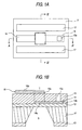
- Figs. 1A to 1C are schematic views showing a thin-film piezoelectric resonator according to a first embodiment of the invention.
- Fig. 1A is a plan view of the thin-film piezoelectric resonator .
- Figs . 1B and 1C are sectional views taken along the line A-A' and the line B-B' in Fig. 1A.
- the resonator according to this embodiment includes a substrate 11 having a vibration space S, and an upper barrier layer 12 and a lower barrier layer 13 provided on upper and lower surfaces of the substrate 11 respectively.
- the resonator further includes a lower electrode 14 provided on the upper barrier layer 12, a piezoelectric thin film 15 provided on the lower electrode 14, and an upper electrode 16 and ground electrodes 17 provided on the piezoelectric thin film 15.
- the lower electrode is electrically connected to a signal electrode through a through-hole 15a provided in the piezoelectric thin film to thereby form a resonator of a coplanar structure.
- the upper electrode 16 and the lower electrode 14 have portions for resonating the upper electrode 16 and the lower electrode 14 (hereinafter referred to as resonant portions 16a and 14a respectively), and portions of the upper and lower electrodes 16 and 14 except the resonant portions 16a and 14a (hereinafter referred to as lead-out portions 16b and 14b respectively). Configuration is made so that the electrode thickness of at least one part of the lead-out portion 16b or 14b in at least one of the upper and lower electrodes 16 and 14 is larger than the electrode thickness of the resonant portion 16a or 14a formed to be continued from the lead-out portion.
- the term "formed to be continued" used herein means that the resonant portion and the lead-out portion are formed on the same plane and electrically connected to each other. That is, in Figs. 1A and 1B, for example, the lead-out portion 16b and the resonant portion 16a in the upper electrode are formed continuously, and the lead-out portion 14b and the resonant portion 14a in the lower electrode are formed continuously.
- configuration may be made so that the electrode thickness of at least part of the ground electrodes is larger than the electrode thickness of the resonant portion of the upper or lower electrode formed on the same plane with the ground electrodes as shown in Fig. 1C.
- Figs. 1A and 1B show the case where the electrode thickness of all the lead-out portion 16b of the upper electrode 16 ismade large, part of the lead-out portion 16b may be thickened. Alternatively, all or part of the ground electrodes 17 may be thickened. Or the electrode thickness of at least one of the upper electrode 16, the lower electrode 14 and the ground electrodes 17 may be made large. When part of the lead-out portion or the ground electrodes is thickened, for example, configurationmaybe made so that a neighborhood of an end portion of the lead-out portion is thickened so as to be provided as a pad for connecting an electrically connecting wire or the like.
- each resonant portion is limited in order to obtain a required resonant frequency.
- Each of the lead-out portions and the ground electrodes can have an arbitrary thickness because the lead-out portions and the ground electrodes have no relation to resonance. Accordingly, in order to reduce insertion loss affected by electric resistance of the electrodes, the electrode thickness of each of the lead-out portions of the upper and lower electrodes and the ground electrodes may be formed so as to be as large as possible to reduce electric resistance of these portions to thereby reduce insertion loss of the resonator.
- the substrate 11 has a cavity S provided correspondingly to a region in which the resonator T is disposed.
- the cavity S is shaped like a rectangle in top view.
- the thickness of the substrate 11 is in a range of from about 100 ⁇ m to about 1000 ⁇ m.
- the upper barrier layer 12 is an electrically insulating layer for separating the substrate 11 and the lower electrode 14 from each other so that the lower electrode 14 can be disposed in a region corresponding to the cavity S of the substrate 11.
- silicon nitride (SiN x ), SiO 2 or the like may be used as the material of the upper barrier layer 12.
- the thickness of the upper barrier layer 12 is in a range of from about 0.03 ⁇ m to about 0.5 ⁇ m.
- the lower barrier layer 13 is formed as a predetermined pattern for providing the cavity S .
- silicon nitride (SiN x ), SiO 2 or the like may be used as the material of the lower barrier layer 13.
- the thickness of the lower barrier layer 13 is in a range of from about 0.03 ⁇ m to about 0.5 ⁇ m.
- the piezoelectric thin film 15 is a thin film having piezoelectric characteristic.
- zinc oxide (ZnO), lead zirconate titanate (Pb (Zr, Ti) O 3 ) (hereinafter referred to as PZT), aluminum nitride (AlN) or the like may be used as the material of the piezoelectric thin film 15.
- the thickness of the piezoelectric thin film 15 is preferably selected to be not larger than 5 ⁇ m. This is because the operating frequency is lowered if the piezoelectric thin film 15 is too thick. Accordingly, it is preferable that the piezoelectric thin film 15 is formed to be as thin as possible so that the operating frequency shifts to the higher-frequency side. In consideration of the problem on fabrication, reliability, etc., the lower limit of the thickness is set at about 0.05 ⁇ m.
- a buffer layer (not shown) may be provided between the upper barrier layer and the lower electrode layer.
- SiO 2 /TiO 2 , ZrO 2 or the like may be used as the material of the buffer layer.
- the thickness of the buffer layer may be selected to be in a range of from about 0.03 ⁇ m to about 0.5 ⁇ m.
- a metal such as Al, Pt, Au, Ag, Cr, Cu, Ti, etc. may be used as the material of each of the lower and upper electrodes 14 and 16.
- an adhesive layer may be formed on the piezoelectric thin film from the point of view of improving adhesion between the electrode material and the piezoelectric thin film.
- a chromium (Cr) layer may be formed as an adhesive layer and a gold (Au) layer may be laminated on the whole surface of the chromium layer so as to form a two-layered structure.
- the thickness of at least part of the lead-out portion is larger than the thickness of the resonant portion.
- the thickness of the resonant portion is decided on the frequency of the resonator and is generally in a range of from about 0.03 ⁇ m to about 1 ⁇ m. On the other hand, when the thickness of at least part of the lead-out portion is made large, the upper limit of the thickness is set at about 5 ⁇ m.
- each ground electrode 17 is shaped like a rectangle long in one direction on the upper surface of the piezoelectric thin film but the shape of each ground electrode 17 is not limited thereto.
- the upper limit of the thickness of each ground electrode 17 is set at about 5 ⁇ m.
- Figs. 1A and 1B the resonant portion 14a provided in the neighborhood of the left end portion of the lower electrode 14 and the resonant portion 16a provided in the neighborhood of the right end portion of the upper electrode 16 are disposed opposite to each other through the piezoelectric thin film 15. These resonant portions 14a and 16a and the piezoelectric thin film 15 form the resonator T.
- Fig. 1A shows the case where the resonant portion 14a of the lower electrode 14 is slightly different in size from the resonant portion 16a of the upper electrode 16 for the sake of convenience, the size of the resonant portion 14a is practically equal to the size of the resonant portion 16a.
- the piezoelectric thin film 15 has a through-hole 15a provided in a position corresponding to the neighborhood of an end of the lower electrode 14 opposite to the end portion where the resonant portion 14a is provided.
- the lower electrode 14 is connected to a signal conductor portion (not shown) by a bonding wire or the like (not shown) passing through the through-hole 15a.
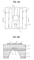
- Figs. 2A and 2B are schematic views showing a filter according to a second embodiment of the invention.
- Fig. 2A is a plan view of the filter.
- Fig. 2B is a sectional view taken along the line A-A' in Fig. 2A.
- the filter is formed as a ladder filter in which resonators are connected in series and inparallel as shown in Fig. 3.
- the basic layer structure or the like is the same as in the first embodiment shown in Figs. 1A and 1B. Although the description of duplicated parts will be omitted here, the structure of electrodes as a different structure will be described below.
- Lower electrodes 24A and 24B are disposed left and right in Figs. 2A and 2B.
- a lower electrode 24C is disposed below the lower electrodes 24A and 24B in Fig. 2A.
- Each of the lower electrodes 24A and 24B is substantially shaped like a rectangle in plan view so that the width of a neighborhood of an end portion of the lower electrode adj acent to an end portion of the other lower electrode is slightly larger than the width of the other portion.
- the lower electrode 24C is shaped like a rectangle long in one direction in plan view.
- An upper electrode 26 is substantially shaped like a T figure in plan view.
- the upper electrode 26 has three resonant portions 26a, 26b and 26c in the neighborhoods of end portions of the T figure, and a lead-out portion 26d.
- the resonant portions 26a and 26b are slightly wider than the other portions.
- the lower electrode 24A serves also as an input terminal of the filter.
- the lower electrode 24B serves also as an output terminal of the filter.
- the lower electrode 24C is grounded.
- the lower electrodes 24A, 24B and 24C have resonant portions 24Aa, 24Ba and 24Ca, and lead-out portions 24Ab, 24Bb, 24Cb and 24Cc respectively.
- the filter according to this embodiment is formed so that the electrode thickness of at least part of the lead-out portion 26d, 24Ab, 24Bb, 24Cb or 24Cc in each of the upper electrode 26 and the lower electrodes 24A, 24B and 24C is larger than the electrode thickness of the resonant portion 26a, 26b, 26c, 24Aa, 24Ba or 24Ca formed to be continued from the lead-out portion.
- Figs. 2A and 2B show the case where the whole surface of the lead-out portion 26d of the upper electrode 26 is formed to be thicker than the resonant portions 26a, 26b and 26c of the upper electrode 26, part of the lead-out portion 26d may be formed to be thicker. All or part of at least one of the lead-out portions of the lower electrodes 24A, 24B and 24C may be thickened. At least one of the upper electrode 26 and the lower electrodes 24A, 24B and 24C may be thickened.
- the resonant portion 24Aa provided in a neighborhood of the right end portion of the lower electrode 24A and the resonant portion 26a provided in a neighborhood of the left end portion of the upper electrode 26 are disposed opposite to each other through a piezoelectric thin film 25.
- These resonant portions 24Aa and 26a of the electrodes 24A and 26 and the piezoelectric thin film 25 form a series resonator T1 on the input terminal side of the filter.
- the resonant portion 24Ba provided in a neighborhood of the left end portion of the lower electrode 24B and the resonant portion 26b provided in a neighborhood of the right end portion of the upper electrode 26 are disposed opposite to each other through the piezoelectric thin film 25.
- These resonant portions 24Ba and 26b of the electrodes 24B and 26 and the piezoelectric thin film 25 form a series resonator T2 on the output terminal side of the filter.
- FIG. 2A shows the case where the resonant portions 24Aa and 24Ba of the lower electrodes 24A and 24B are different in size from the resonant portions 26a and 26b of the upper electrode 26 for the sake of convenience, the resonant portions 24Aa and 24Ba are practically equal in size to the resonant portions 26a and 26b.
- the resonant portion 24Ca provided in a neighborhood of the center of the lower electrode 24C and the resonant portion 26c provided in a neighborhood of the lower end portion of the upper electrode 26 are disposed opposite to each other through the piezoelectric thin film 25. These resonant portions 24Ca and 26c of the electrodes 24C and 26 and the piezoelectric thin film 25 form a parallel resonator T3 in the filter.
- the piezoelectric thin film 25 has through-holes 25a, 25b, 25c and 25d provided in positions corresponding to the neighborhoods of end portions of the lower electrodes 24A and 24B opposite to the end portions where the resonant portions 24Aa and 24Ba are provided and in positions corresponding to the neighborhoods of opposite end portions of the lower electrode 24C, respectively.
- the lower electrodes 24A and 24B are connected to signal conductor portions (not shown) by bonding wires or the like (not shown) passing through the through-holes 25a and 25b respectively.
- the lower electrode 24C is connected to a ground conductor portion (not shown) by bonding wires or the like (not shown) passing through the through-holes 25c and 25d.
- the resonators according to this embodiment may be formed to function as a duplexer.
- the resonator according to the embodiment shown in Figs . 1A and 1B may be basically fabricated by the same fabricating method except difference in electrode structure.
- silicon nitride (SiN x ) with a predetermined thickness is deposited by a chemical vapor deposition method on each of upper and lower surfaces of a bare Si wafer serving as the substrate 21.
- SiN x formed on the upper surface of the Si wafer forms the upper barrier layer 22.
- SiN x formed on the lower surface of the Si wafer is processed into a predetermined pattern by photolithography and reactive ion-etching to thereby form the lower barrier layer 23.
- the lower electrodes 24A, 24B and 24C are formed by a so-called lift-off process accordingtothe following procedure .
- a predetermined pattern of photo resist is formed by photolithography.
- metals as electrode materials e.g., chromium and gold (Cu/Au) with predetermined thicknesses are deposited by sputtering.
- chromium and gold Cu/Au
- a 10 nm-thick chromium layer and a 100 nm-thick gold layer are formed.
- Cr is used as an adhesive layer.
- the patterned photo resist and Cu/Au formed thereon are removed with a solvent such as acetone to thereby obtain the lower electrodes 24A, 24B and 24C.
- a piezoelectric material for forming the piezoelectric thin film 25 e.g., zinc oxide (ZnO) with a predetermined thickness is formed by sputtering.
- the piezoelectric thin film 25 is etched with acetic acid to form through-holes 25a, 25b, 25c and 25d for connecting bonding wires to the lower electrodes 24A, 24B and 24C respectively.
- the upper electrode 26 is formedbya lift-off process.
- a mask 41 shown in Fig. 4 is used so that the electrode is formed by sputtering Cr/Au
- a mask 42 shown in Fig. 4 is used so that a portion of overlap between the masks 41 and 42 in the electrode can be thickened by sputtering Cr/Au.
- the shapes of masks can be selected so that a predetermined portion of the electrode is thickened.
- the Si wafer is etched with a KOH solution from the lower barrier layer on the back.
- the filter is fabricated completely.
- the lower electrodes may be thickened in the same electrode fabricating procedure as described above or the upper and lower electrodes may be thickened.
- Figs. 5A and 5B are schematic views showing a thin-film piezoelectric resonator according to a third embodiment of the invention.
- Fig. 5A is a plan view of the thin-film piezoelectric resonator.
- Fig. 5B is a sectional view taken along the line A-A' in Fig. 5A.
- the basic layer structure or the like is the same as in the first embodiment shown in Figs. 1A and 1B. The description of duplicated parts will be omitted. Other parts than an upper electrode, a lower electrode and ground electrodes are not shown in Figs. 5A and 5B. The structure of electrodes as a different structure will be described below.
- At least one of the upper electrode 34 and the lower electrode 36 is formed so that the electrode material of the resonant portion 34a (36a) is different from the electrode material of the lead-out portion 34b (36b) formed to be continued from the resonant portion 34a (36a).
- the resonant portion and the lead-out port ion are connected to each other so as to partially overlap each other in the connection portion. That is, at least part of the lead-out portion 34b is formedby stacking an electrode material different from that of the resonant portion 34a, and one electrode of the stacked materials is continued from the resonant portion 34a. This is for the necessity of ensuring electric connectionbecause insertion loss increases if electric connection in the connection portion is insufficient.
- configuration may be made so that the electrode material of the ground electrodes 37 is made different from the electrode material of the resonant portion 34a or 36a of the upper or lower electrode 34 or 36.
- a material which is low both in Poisson's ratio and in density is preferably used as the electrode material of the resonant portions 34a and 36a.
- a material which is low in specific resistance is preferably used as the electrode material of the lead-out portions 34b and 36b or the ground electrodes 37.
- aluminum (Al) is preferably used as the electrode material of the resonant portions whereas copper (Cu) or silver (Ag) is preferably used as the electrode material of the lead-out portions.
- Table 1 shows characteristics of electrode materials.
- Figs. 6A to 6C show impedance-frequency characteristics of electrode materials.
- the impedance-frequency characteristic shown in Figs. 6A to 6C is measured for different electrode materials, in a thin-film piezoelectric resonator having a 0.1 ⁇ m-thick upper barrier layer (SiN x ), a 0.1 ⁇ m-thick lower electrode, a 1 ⁇ m-thick piezoelectric thin film (ZnO), and a 0.1 ⁇ m-thick upper electrode.
- configuration may be preferably made so that the electrode thickness of at least part of the lead-out portion is larger than the electrode thickness of the resonant portion formed to be continued from the lead-out portion in the same manner as in the first embodiment of the invention.
- configuration may be preferably made so that the electrode thickness of at least part of the ground electrodes is larger than the electrode thickness of the resonant portion of the upper or lower electrode formed on the same plane with the ground electrodes.
- configuration maybe made so that the electrode material of each resonant portion in at least one of the lower and upper electrodes is different from the electrode material of the lead-out portion formed to be continued from the resonant portion.
- resonators according to this embodiment may be formed to function as a duplexer.
- silicon nitride (SiN x ) with a predetermined thickness is deposited by a chemical vapor deposition method on each of upper and lower surfaces of a bare Si wafer serving as the substrate.
- SiN x formed on the upper surface of the Si wafer forms the upper barrier layer.
- SiN x formed on the lower surface of the Si wafer is processed into a predetermined pattern by photolithography and reactive ion-etching to thereby form the lower barrier layer. (The layer structure is the same as in Figs. 1A and 1B).
- the lower electrode 36 is formed by a so-called lift-off process according to the following procedure.
- a predetermined pattern of photo resist is formed by photolithography.
- metalsaselectrode materials e.g., chromium and gold (Cu/Au) with a thickness of 10 nm and a thickness of 100 nm respectively are deposited by sputtering.
- Cr is used as an adhesive layer.
- the patterned photo resist and Cu/Au formed thereon are removed with a solvent such as acetone to thereby obtain the lower electrode 36.
- a piezoelectric material for forming the piezoelectric thin film 35 e.g., zinc oxide (ZnO) with a predetermined thickness is formed by sputtering.
- the piezoelectric thin film is etched with acetic acid to form a through-hole 35a for connecting a bonding wire to the lower electrode 36.
- the upper electrode 34 is formedby a lift-off process.
- a mask 43 shown in Fig. 7 is used so that the resonant portion 34a of the electrode is formed by sputtering Al
- a mask 44 shown in Fig. 7 is used so that the lead-out portion 34b of the electrode is formed by sputtering Cr/Au.
- the lift-off process may be repeated twice in the same manner as described above while the masks of predetermined shapes are used.
- the Si wafer is etched with a KOH solution from the lower barrier layer on the back.
- the resonator is fabricated completely.
- Fig. 8 is a schematic sectional view showing a thin-film piezoelectric resonator according to a fourth embodiment of the invention.
- the basic layer structure or the like is the same as in the first embodiment shown in Figs. 1A and 1B except that the vibration space is replaced by a cavity 48 provided between a lower barrier layer 42 and a substrate 41.
- upper and lower electrodes 46 and 44 are provided on upper and lower surfaces of a piezoelectric thin film 45 respectively and configuration is made so that a lead-out portion of the upper electrode is thicker than a resonant portion of the upper electrode, in the same manner as in Figs. 1A and 1B.
- configuration may be made so that the electrode material of the resonant portion is different from the electrode material of the lead-out portion formed to be continued from the resonant portion, in the same manner as in the third embodiment.
- Fig. 9 is a schematic sectional view showing a thin-film piezoelectric resonator according to a fifth embodiment of the invention.
- the basic layer structure or the like is the same as in the first embodiment shown in Figs. 1A and 1B except that the vibration space is replaced by an acoustic multi-layer film of layers 58a and 58b provided between a lower electrode 54 and a substrate 51.
- the acoustic multi-layer film is formed by lamination of layers of a high acoustic impedance material such as aluminum nitride and layers of a low acoustic impedance material such as silicon oxide.
- the acoustic multi-layer film may be composed of three or more layers so that layers of a high acoustic impedance material and layers of a low acoustic impedance material are laminated alternately.
- upper and lower electrodes 56 and 54 are provided on upper and lower surfaces of a piezoelectric thin film 55 respectively and configuration is made so that a lead-out portion of the upper electrode is thicker than a resonant portion of the upper electrode, in the same manner as in Figs. 1A and 1B.
- configuration may be made so that the electrode material of the resonant portion is different from the electrode material of the lead-out portion formed to be continued from the resonant portion, in the same manner as in the third embodiment.
- the filter, the duplexer and the method for fabricating the thin-film piezoelectric resonator according to the invention insertion loss can be reduced. In addition, ripples can be reduced.
Landscapes
- Physics & Mathematics (AREA)
- Acoustics & Sound (AREA)
- Engineering & Computer Science (AREA)
- Manufacturing & Machinery (AREA)
- Chemical & Material Sciences (AREA)
- Crystallography & Structural Chemistry (AREA)
- Piezo-Electric Or Mechanical Vibrators, Or Delay Or Filter Circuits (AREA)
Applications Claiming Priority (2)
| Application Number | Priority Date | Filing Date | Title |
|---|---|---|---|
| JP2002282727A JP4128836B2 (ja) | 2002-09-27 | 2002-09-27 | 薄膜圧電共振子、それを用いたフィルタ及びデュプレクサ |
| JP2002282727 | 2002-09-27 |
Publications (2)
| Publication Number | Publication Date |
|---|---|
| EP1406383A2 true EP1406383A2 (de) | 2004-04-07 |
| EP1406383A3 EP1406383A3 (de) | 2006-01-04 |
Family
ID=31987118
Family Applications (1)
| Application Number | Title | Priority Date | Filing Date |
|---|---|---|---|
| EP03021868A Withdrawn EP1406383A3 (de) | 2002-09-27 | 2003-09-26 | Dünnfilmresonator und Verfahren zum Herstellen desselben |
Country Status (3)
| Country | Link |
|---|---|
| US (1) | US6977563B2 (de) |
| EP (1) | EP1406383A3 (de) |
| JP (1) | JP4128836B2 (de) |
Cited By (2)
| Publication number | Priority date | Publication date | Assignee | Title |
|---|---|---|---|---|
| EP1653612A3 (de) * | 2004-10-28 | 2007-06-27 | Fujitsu Media Devices Limited | Piezoelektrischer Dünnschichtresonator und Filter mit einem derartigen Resonator |
| EP1890380A1 (de) | 2006-08-16 | 2008-02-20 | Samsung Electronics Co., Ltd. | Resonator und Herstellungsverfahren dafür |
Families Citing this family (65)
| Publication number | Priority date | Publication date | Assignee | Title |
|---|---|---|---|---|
| JPH075734U (ja) * | 1993-07-05 | 1995-01-27 | 株式会社佐々木製作所 | シルク印刷用刷板の取付装置 |
| GB0029090D0 (en) * | 2000-11-29 | 2001-01-10 | Univ Cranfield | Improvements in or relating to filters |
| US7275292B2 (en) | 2003-03-07 | 2007-10-02 | Avago Technologies Wireless Ip (Singapore) Pte. Ltd. | Method for fabricating an acoustical resonator on a substrate |
| KR20050035905A (ko) * | 2003-10-07 | 2005-04-20 | 삼성전기주식회사 | 단일 칩 fbar 듀플렉서 |
| US7362198B2 (en) | 2003-10-30 | 2008-04-22 | Avago Technologies Wireless Ip (Singapore) Pte. Ltd | Pass bandwidth control in decoupled stacked bulk acoustic resonator devices |
| US7332985B2 (en) | 2003-10-30 | 2008-02-19 | Avago Technologies Wireless Ip (Singapore) Pte Ltd. | Cavity-less film bulk acoustic resonator (FBAR) devices |
| EP1528677B1 (de) | 2003-10-30 | 2006-05-10 | Agilent Technologies, Inc. | Akustisch gekoppelter Dünnschicht-Transformator mit zwei piezoelektrischen Elementen, welche entgegengesetzte C-Axen Orientierung besitzten |
| US7019605B2 (en) | 2003-10-30 | 2006-03-28 | Larson Iii John D | Stacked bulk acoustic resonator band-pass filter with controllable pass bandwidth |
| US6946928B2 (en) | 2003-10-30 | 2005-09-20 | Agilent Technologies, Inc. | Thin-film acoustically-coupled transformer |
| US7615833B2 (en) | 2004-07-13 | 2009-11-10 | Avago Technologies Wireless Ip (Singapore) Pte. Ltd. | Film bulk acoustic resonator package and method of fabricating same |
| US7388454B2 (en) * | 2004-10-01 | 2008-06-17 | Avago Technologies Wireless Ip Pte Ltd | Acoustic resonator performance enhancement using alternating frame structure |
| US8981876B2 (en) | 2004-11-15 | 2015-03-17 | Avago Technologies General Ip (Singapore) Pte. Ltd. | Piezoelectric resonator structures and electrical filters having frame elements |
| US7202560B2 (en) | 2004-12-15 | 2007-04-10 | Avago Technologies Wireless Ip (Singapore) Pte. Ltd. | Wafer bonding of micro-electro mechanical systems to active circuitry |
| US7791434B2 (en) | 2004-12-22 | 2010-09-07 | Avago Technologies Wireless Ip (Singapore) Pte. Ltd. | Acoustic resonator performance enhancement using selective metal etch and having a trench in the piezoelectric |
| DE102005004435B4 (de) * | 2005-01-31 | 2006-10-19 | Infineon Technologies Ag | Baw-resonator |
| US7427819B2 (en) | 2005-03-04 | 2008-09-23 | Avago Wireless Ip Pte Ltd | Film-bulk acoustic wave resonator with motion plate and method |
| US7369013B2 (en) | 2005-04-06 | 2008-05-06 | Avago Technologies Wireless Ip Pte Ltd | Acoustic resonator performance enhancement using filled recessed region |
| US7436269B2 (en) | 2005-04-18 | 2008-10-14 | Avago Technologies Wireless Ip (Singapore) Pte. Ltd. | Acoustically coupled resonators and method of making the same |
| JP4629492B2 (ja) | 2005-05-10 | 2011-02-09 | 太陽誘電株式会社 | 圧電薄膜共振子およびフィルタ |
| US7868522B2 (en) | 2005-09-09 | 2011-01-11 | Avago Technologies Wireless Ip (Singapore) Pte. Ltd. | Adjusted frequency temperature coefficient resonator |
| US7391286B2 (en) | 2005-10-06 | 2008-06-24 | Avago Wireless Ip Pte Ltd | Impedance matching and parasitic capacitor resonance of FBAR resonators and coupled filters |
| US7525398B2 (en) | 2005-10-18 | 2009-04-28 | Avago Technologies General Ip (Singapore) Pte. Ltd. | Acoustically communicating data signals across an electrical isolation barrier |
| US7425787B2 (en) | 2005-10-18 | 2008-09-16 | Avago Technologies Wireless Ip (Singapore) Pte. Ltd. | Acoustic galvanic isolator incorporating single insulated decoupled stacked bulk acoustic resonator with acoustically-resonant electrical insulator |
| US7675390B2 (en) | 2005-10-18 | 2010-03-09 | Avago Technologies Wireless Ip (Singapore) Pte. Ltd. | Acoustic galvanic isolator incorporating single decoupled stacked bulk acoustic resonator |
| US7737807B2 (en) | 2005-10-18 | 2010-06-15 | Avago Technologies Wireless Ip (Singapore) Pte. Ltd. | Acoustic galvanic isolator incorporating series-connected decoupled stacked bulk acoustic resonators |
| US7423503B2 (en) | 2005-10-18 | 2008-09-09 | Avago Technologies Wireless Ip (Singapore) Pte. Ltd. | Acoustic galvanic isolator incorporating film acoustically-coupled transformer |
| US7463499B2 (en) | 2005-10-31 | 2008-12-09 | Avago Technologies General Ip (Singapore) Pte Ltd. | AC-DC power converter |
| US7561009B2 (en) | 2005-11-30 | 2009-07-14 | Avago Technologies General Ip (Singapore) Pte. Ltd. | Film bulk acoustic resonator (FBAR) devices with temperature compensation |
| US7612636B2 (en) | 2006-01-30 | 2009-11-03 | Avago Technologies Wireless Ip (Singapore) Pte. Ltd. | Impedance transforming bulk acoustic wave baluns |
| JP4963193B2 (ja) | 2006-03-07 | 2012-06-27 | 日本碍子株式会社 | 圧電薄膜デバイス |
| US7746677B2 (en) | 2006-03-09 | 2010-06-29 | Avago Technologies Wireless Ip (Singapore) Pte. Ltd. | AC-DC converter circuit and power supply |
| US7479685B2 (en) | 2006-03-10 | 2009-01-20 | Avago Technologies General Ip (Singapore) Pte. Ltd. | Electronic device on substrate with cavity and mitigated parasitic leakage path |
| JP4811931B2 (ja) * | 2006-05-10 | 2011-11-09 | 日本碍子株式会社 | 圧電薄膜デバイス |
| US7629865B2 (en) | 2006-05-31 | 2009-12-08 | Avago Technologies Wireless Ip (Singapore) Pte. Ltd. | Piezoelectric resonator structures and electrical filters |
| JP2007335977A (ja) * | 2006-06-12 | 2007-12-27 | Toshiba Corp | 電子素子 |
| US7508286B2 (en) | 2006-09-28 | 2009-03-24 | Avago Technologies Wireless Ip (Singapore) Pte. Ltd. | HBAR oscillator and method of manufacture |
| JP4838093B2 (ja) * | 2006-10-25 | 2011-12-14 | 太陽誘電株式会社 | 圧電薄膜共振器およびフィルタ |
| US7791435B2 (en) | 2007-09-28 | 2010-09-07 | Avago Technologies Wireless Ip (Singapore) Pte. Ltd. | Single stack coupled resonators having differential output |
| US7732977B2 (en) | 2008-04-30 | 2010-06-08 | Avago Technologies Wireless Ip (Singapore) | Transceiver circuit for film bulk acoustic resonator (FBAR) transducers |
| US7855618B2 (en) | 2008-04-30 | 2010-12-21 | Avago Technologies Wireless Ip (Singapore) Pte. Ltd. | Bulk acoustic resonator electrical impedance transformers |
| JP5161698B2 (ja) * | 2008-08-08 | 2013-03-13 | 太陽誘電株式会社 | 圧電薄膜共振子及びこれを用いたフィルタあるいは分波器 |
| US8902023B2 (en) | 2009-06-24 | 2014-12-02 | Avago Technologies General Ip (Singapore) Pte. Ltd. | Acoustic resonator structure having an electrode with a cantilevered portion |
| US8248185B2 (en) | 2009-06-24 | 2012-08-21 | Avago Technologies Wireless Ip (Singapore) Pte. Ltd. | Acoustic resonator structure comprising a bridge |
| US8193877B2 (en) | 2009-11-30 | 2012-06-05 | Avago Technologies Wireless Ip (Singapore) Pte. Ltd. | Duplexer with negative phase shifting circuit |
| US8796904B2 (en) | 2011-10-31 | 2014-08-05 | Avago Technologies General Ip (Singapore) Pte. Ltd. | Bulk acoustic resonator comprising piezoelectric layer and inverse piezoelectric layer |
| US9243316B2 (en) | 2010-01-22 | 2016-01-26 | Avago Technologies General Ip (Singapore) Pte. Ltd. | Method of fabricating piezoelectric material with selected c-axis orientation |
| US8962443B2 (en) | 2011-01-31 | 2015-02-24 | Avago Technologies General Ip (Singapore) Pte. Ltd. | Semiconductor device having an airbridge and method of fabricating the same |
| US9148117B2 (en) | 2011-02-28 | 2015-09-29 | Avago Technologies General Ip (Singapore) Pte. Ltd. | Coupled resonator filter comprising a bridge and frame elements |
| US9203374B2 (en) | 2011-02-28 | 2015-12-01 | Avago Technologies General Ip (Singapore) Pte. Ltd. | Film bulk acoustic resonator comprising a bridge |
| US9136818B2 (en) | 2011-02-28 | 2015-09-15 | Avago Technologies General Ip (Singapore) Pte. Ltd. | Stacked acoustic resonator comprising a bridge |
| US9154112B2 (en) | 2011-02-28 | 2015-10-06 | Avago Technologies General Ip (Singapore) Pte. Ltd. | Coupled resonator filter comprising a bridge |
| US9048812B2 (en) | 2011-02-28 | 2015-06-02 | Avago Technologies General Ip (Singapore) Pte. Ltd. | Bulk acoustic wave resonator comprising bridge formed within piezoelectric layer |
| US9083302B2 (en) | 2011-02-28 | 2015-07-14 | Avago Technologies General Ip (Singapore) Pte. Ltd. | Stacked bulk acoustic resonator comprising a bridge and an acoustic reflector along a perimeter of the resonator |
| US9425764B2 (en) | 2012-10-25 | 2016-08-23 | Avago Technologies General Ip (Singapore) Pte. Ltd. | Accoustic resonator having composite electrodes with integrated lateral features |
| US9444426B2 (en) | 2012-10-25 | 2016-09-13 | Avago Technologies General Ip (Singapore) Pte. Ltd. | Accoustic resonator having integrated lateral feature and temperature compensation feature |
| US8575820B2 (en) | 2011-03-29 | 2013-11-05 | Avago Technologies General Ip (Singapore) Pte. Ltd. | Stacked bulk acoustic resonator |
| US8350445B1 (en) | 2011-06-16 | 2013-01-08 | Avago Technologies Wireless Ip (Singapore) Pte. Ltd. | Bulk acoustic resonator comprising non-piezoelectric layer and bridge |
| US8922302B2 (en) | 2011-08-24 | 2014-12-30 | Avago Technologies General Ip (Singapore) Pte. Ltd. | Acoustic resonator formed on a pedestal |
| US9602076B1 (en) * | 2015-05-19 | 2017-03-21 | Qorvo Us, Inc. | Resonators with balancing capacitor |
| JP2017092535A (ja) * | 2015-11-02 | 2017-05-25 | セイコーエプソン株式会社 | 圧電素子、超音波プローブ、超音波測定装置及び圧電素子の製造方法 |
| JP6757594B2 (ja) * | 2016-05-18 | 2020-09-23 | 太陽誘電株式会社 | 圧電薄膜共振器、フィルタおよびマルチプレクサ |
| CN109474254B (zh) | 2018-10-31 | 2020-12-08 | 武汉衍熙微器件有限公司 | 一种声波器件及其制作方法 |
| CN112452694A (zh) * | 2020-09-23 | 2021-03-09 | 长江大学 | 多频压电式微型超声换能器单元、阵列和方法 |
| JP7491408B2 (ja) * | 2020-12-11 | 2024-05-28 | 株式会社村田製作所 | 圧電振動子、圧電発振器、及び圧電振動子製造方法 |
| WO2026078949A1 (ja) * | 2024-10-07 | 2026-04-16 | 株式会社村田製作所 | 圧電振動素子 |
Family Cites Families (15)
| Publication number | Priority date | Publication date | Assignee | Title |
|---|---|---|---|---|
| US4320365A (en) | 1980-11-03 | 1982-03-16 | United Technologies Corporation | Fundamental, longitudinal, thickness mode bulk wave resonator |
| JPS60189307A (ja) | 1984-03-09 | 1985-09-26 | Toshiba Corp | 圧電薄膜共振器およびその製造方法 |
| JPH0446411A (ja) * | 1990-06-14 | 1992-02-17 | Fujitsu Ltd | 水晶振動子、該振動子を備えた発振器モジュール及び該モジュールの製造方法 |
| WO1999037023A1 (en) | 1998-01-16 | 1999-07-22 | Mitsubishi Denki Kabushiki Kaisha | Thin film pietoelectric element |
| JP2000278078A (ja) | 1999-03-29 | 2000-10-06 | Kyocera Corp | 圧電共振子 |
| JP2001211052A (ja) * | 2000-01-26 | 2001-08-03 | Murata Mfg Co Ltd | 圧電共振子 |
| GB0012439D0 (en) * | 2000-05-24 | 2000-07-12 | Univ Cranfield | Improvements to filters |
| US6674291B1 (en) * | 2000-10-30 | 2004-01-06 | Agere Systems Guardian Corp. | Method and apparatus for determining and/or improving high power reliability in thin film resonator devices, and a thin film resonator device resultant therefrom |
| GB0029090D0 (en) * | 2000-11-29 | 2001-01-10 | Univ Cranfield | Improvements in or relating to filters |
| US6509813B2 (en) * | 2001-01-16 | 2003-01-21 | Nokia Mobile Phones Ltd. | Bulk acoustic wave resonator with a conductive mirror |
| US6601276B2 (en) * | 2001-05-11 | 2003-08-05 | Agere Systems Inc. | Method for self alignment of patterned layers in thin film acoustic devices |
| JP2005236337A (ja) * | 2001-05-11 | 2005-09-02 | Ube Ind Ltd | 薄膜音響共振器及びその製造方法 |
| JP3954395B2 (ja) * | 2001-10-26 | 2007-08-08 | 富士通株式会社 | 圧電薄膜共振子、フィルタ、および圧電薄膜共振子の製造方法 |
| US6657517B2 (en) * | 2001-12-20 | 2003-12-02 | Agere Systems, Inc. | Multi-frequency thin film resonators |
| US6767749B2 (en) * | 2002-04-22 | 2004-07-27 | The United States Of America As Represented By The Secretary Of The Navy | Method for making piezoelectric resonator and surface acoustic wave device using hydrogen implant layer splitting |
-
2002
- 2002-09-27 JP JP2002282727A patent/JP4128836B2/ja not_active Expired - Lifetime
-
2003
- 2003-09-26 US US10/670,234 patent/US6977563B2/en not_active Expired - Lifetime
- 2003-09-26 EP EP03021868A patent/EP1406383A3/de not_active Withdrawn
Cited By (5)
| Publication number | Priority date | Publication date | Assignee | Title |
|---|---|---|---|---|
| EP1653612A3 (de) * | 2004-10-28 | 2007-06-27 | Fujitsu Media Devices Limited | Piezoelektrischer Dünnschichtresonator und Filter mit einem derartigen Resonator |
| EP2259425A1 (de) * | 2004-10-28 | 2010-12-08 | Taiyo Yuden Co., Ltd. | Piezoelektrischer Dünnschichtresonator und Filter mit einem derartigen Resonator |
| US7884527B2 (en) | 2004-10-28 | 2011-02-08 | Taiyo Yuden Co., Ltd. | Piezoelectric thin-film resonator and filter using the same |
| EP1890380A1 (de) | 2006-08-16 | 2008-02-20 | Samsung Electronics Co., Ltd. | Resonator und Herstellungsverfahren dafür |
| US7795692B2 (en) | 2006-08-16 | 2010-09-14 | Samsung Electronics Co., Ltd. | Resonator and fabrication method thereof |
Also Published As
| Publication number | Publication date |
|---|---|
| EP1406383A3 (de) | 2006-01-04 |
| US20040140865A1 (en) | 2004-07-22 |
| US6977563B2 (en) | 2005-12-20 |
| JP4128836B2 (ja) | 2008-07-30 |
| JP2004120494A (ja) | 2004-04-15 |
Similar Documents
| Publication | Publication Date | Title |
|---|---|---|
| US6977563B2 (en) | Thin-film piezoelectric resonator and method for fabricating the same | |
| US7567024B2 (en) | Methods of contacting the top layer of a BAW resonator | |
| EP1914888B1 (de) | Herstellungsverfahren für ein Abzweigfilter | |
| US7649304B2 (en) | Piezoelectric resonator and piezoelectric filter | |
| KR100698985B1 (ko) | 필터 및 필터의 제조 방법 | |
| JP4719683B2 (ja) | ラダー型薄膜バルク音響波フィルタ | |
| JP4426748B2 (ja) | 単一の基板上で異なった中心周波数を有するバルク音響波フィルタ、およびそれを提供する方法 | |
| JP3996379B2 (ja) | 圧電共振子を含むフィルタ構造および構成 | |
| KR100789302B1 (ko) | 압전 박막 공진자, 필터, 및 압전 박막 공진자의 제조 방법 | |
| US20020089393A1 (en) | Monolithic fbar duplexer and method of making the same | |
| JP2008035358A (ja) | 薄膜圧電バルク波共振器及びそれを用いた高周波フィルタ | |
| JP2005057332A (ja) | フィルタ装置およびそれを用いた分波器 | |
| JP2004515149A (ja) | フィルタの、もしくはフィルタに関連する改善 | |
| CN109167585B (zh) | 体声波谐振器及其制作方法、滤波器 | |
| KR100771345B1 (ko) | 압전 박막 공진자 및 필터 | |
| CN113541636B (zh) | 一种声波谐振器及其制备方法 | |
| JP3952464B2 (ja) | デュプレクサ | |
| US7623007B2 (en) | Device including piezoelectric thin film and a support having a vertical cross-section with a curvature | |
| JP2001156582A (ja) | 圧電共振子 | |
| JP7794615B2 (ja) | 圧電薄膜共振器およびその製造方法 | |
| WO2007129696A1 (ja) | 送受切換器 | |
| KR20010029007A (ko) | 탄성파 소자의 제조방법 및 그에 따라 제조된 탄성파 소자 | |
| CN115714587A (zh) | 一种滤波器以及滤波器的制备方法 |
Legal Events
| Date | Code | Title | Description |
|---|---|---|---|
| PUAI | Public reference made under article 153(3) epc to a published international application that has entered the european phase |
Free format text: ORIGINAL CODE: 0009012 |
|
| AK | Designated contracting states |
Kind code of ref document: A2 Designated state(s): AT BE BG CH CY CZ DE DK EE ES FI FR GB GR HU IE IT LI LU MC NL PT RO SE SI SK TR |
|
| AX | Request for extension of the european patent |
Extension state: AL LT LV MK |
|
| PUAL | Search report despatched |
Free format text: ORIGINAL CODE: 0009013 |
|
| AK | Designated contracting states |
Kind code of ref document: A3 Designated state(s): AT BE BG CH CY CZ DE DK EE ES FI FR GB GR HU IE IT LI LU MC NL PT RO SE SI SK TR |
|
| AX | Request for extension of the european patent |
Extension state: AL LT LV MK |
|
| 17P | Request for examination filed |
Effective date: 20060315 |
|
| 17Q | First examination report despatched |
Effective date: 20060630 |
|
| AKX | Designation fees paid |
Designated state(s): DE FR GB |
|
| STAA | Information on the status of an ep patent application or granted ep patent |
Free format text: STATUS: THE APPLICATION IS DEEMED TO BE WITHDRAWN |
|
| 18D | Application deemed to be withdrawn |
Effective date: 20090318 |