EP1406476A2 - Circuit de commande d' un gradateur pour ballasts électroniques - Google Patents
Circuit de commande d' un gradateur pour ballasts électroniques Download PDFInfo
- Publication number
- EP1406476A2 EP1406476A2 EP03020633A EP03020633A EP1406476A2 EP 1406476 A2 EP1406476 A2 EP 1406476A2 EP 03020633 A EP03020633 A EP 03020633A EP 03020633 A EP03020633 A EP 03020633A EP 1406476 A2 EP1406476 A2 EP 1406476A2
- Authority
- EP
- European Patent Office
- Prior art keywords
- coupled
- voltage
- rectifier
- circuit
- anode
- Prior art date
- Legal status (The legal status is an assumption and is not a legal conclusion. Google has not performed a legal analysis and makes no representation as to the accuracy of the status listed.)
- Withdrawn
Links
Images


Classifications
-
- H—ELECTRICITY
- H05—ELECTRIC TECHNIQUES NOT OTHERWISE PROVIDED FOR
- H05B—ELECTRIC HEATING; ELECTRIC LIGHT SOURCES NOT OTHERWISE PROVIDED FOR; CIRCUIT ARRANGEMENTS FOR ELECTRIC LIGHT SOURCES, IN GENERAL
- H05B41/00—Circuit arrangements or apparatus for igniting or operating discharge lamps
- H05B41/14—Circuit arrangements
- H05B41/36—Controlling
- H05B41/38—Controlling the intensity of light
- H05B41/39—Controlling the intensity of light continuously
- H05B41/392—Controlling the intensity of light continuously using semiconductor devices, e.g. thyristor
- H05B41/3921—Controlling the intensity of light continuously using semiconductor devices, e.g. thyristor with possibility of light intensity variations
- H05B41/3924—Controlling the intensity of light continuously using semiconductor devices, e.g. thyristor with possibility of light intensity variations by phase control, e.g. using a triac
-
- H—ELECTRICITY
- H05—ELECTRIC TECHNIQUES NOT OTHERWISE PROVIDED FOR
- H05B—ELECTRIC HEATING; ELECTRIC LIGHT SOURCES NOT OTHERWISE PROVIDED FOR; CIRCUIT ARRANGEMENTS FOR ELECTRIC LIGHT SOURCES, IN GENERAL
- H05B41/00—Circuit arrangements or apparatus for igniting or operating discharge lamps
- H05B41/14—Circuit arrangements
- H05B41/36—Controlling
- H05B41/38—Controlling the intensity of light
- H05B41/39—Controlling the intensity of light continuously
- H05B41/392—Controlling the intensity of light continuously using semiconductor devices, e.g. thyristor
- H05B41/3921—Controlling the intensity of light continuously using semiconductor devices, e.g. thyristor with possibility of light intensity variations
- H05B41/3925—Controlling the intensity of light continuously using semiconductor devices, e.g. thyristor with possibility of light intensity variations by frequency variation
-
- H—ELECTRICITY
- H05—ELECTRIC TECHNIQUES NOT OTHERWISE PROVIDED FOR
- H05B—ELECTRIC HEATING; ELECTRIC LIGHT SOURCES NOT OTHERWISE PROVIDED FOR; CIRCUIT ARRANGEMENTS FOR ELECTRIC LIGHT SOURCES, IN GENERAL
- H05B47/00—Circuit arrangements for operating light sources in general, i.e. where the type of light source is not relevant
- H05B47/10—Controlling the light source
- H05B47/175—Controlling the light source by remote control
- H05B47/185—Controlling the light source by remote control via power line carrier transmission
Definitions
- the present invention relates to the general subject of circuits for powering discharge lamps. More particularly, the present invention relates to a dimming control system for electronic ballasts.
- Conventional dimming ballasts for gas discharge lamps include low voltage dimming circuitry that is intended to work in conjunction with an external dimming controller.
- the external dimming controller is connected to special inputs on the ballast via dedicated low voltage control wiring that, for safety reasons, cannot be routed in the same conduit as the AC power wiring.
- the external dimming controller is usually very expensive.
- installation of low voltage control wiring is quite labor-intensive (and thus costly), especially in "retrofit” applications. Because of these disadvantages, considerable efforts have been directed to developing control circuits that can be inserted in series with the AC line, between the AC source and the ballast(s), thereby avoiding the need for additional dimming control wires.
- the resulting approaches are sometimes broadly referred to as "line control" dimming.
- One known type of line control dimming approach involves introducing a notch (i.e., dead-time) into each and every cycle of the AC voltage waveform at or near its zero crossings.
- This approach requires a switching device, such as a triac, in order to create the notch.
- a control circuit measures the time duration of the notch and generates a corresponding dimming control signal for varying the light level produced by the ballast.
- these approaches have a number of drawbacks in cost and performance.
- a significant amount of power is dissipated in the switching device, particularly when multiple ballasts are to be controlled.
- the method itself distorts the line current, resulting in poor power factor and high harmonic distortion, and sometimes produces excessive electromagnetic interference.
- the control circuitry tends to be quite complex and expensive.
- the boost converter may undesirably fall out of regulation during those times.
- the boost converter In order prevent this problem, one would have to design the boost converter to remain in regulation down to very low levels of AC line voltage (e.g., down to about 66% of the nominal AC line voltage), which would add significant cost to the ballasts.
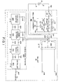
- FIG. 1 describes a dimming control system that includes a wall switch assembly and a ballast having a dimming signal detector circuit, in accordance with a preferred embodiment of the present invention.
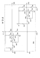
- FIG. 2 describes the AC voltage provided to the ballast under different conditions during the operation of the wall switch assembly illustrated in FIG. 1.
- FIG. 3 describes a 120V/277V detector circuit that is part of the dimming signal detector circuit illustrated in FIG. 1, in accordance with a preferred embodiment of the present invention.
- FIG. 4 describes a zero crossing detector circuit that is part of the dimming signal detector circuit illustrated in FIG. 1, in accordance with a preferred embodiment of the present invention.
- FIG. 5 describes a Schmitt trigger circuit that is part of the dimming signal detector circuit illustrated in FIG. 1, in accordance with a preferred embodiment of the present invention.
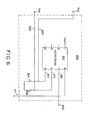
- FIG. 6 describes a controller circuit that is part of the dimming signal detector circuit illustrated in FIG. 1, in accordance with a preferred embodiment of the present invention.
- a dimming control system comprises a wall switch assembly 100 and at least one electronic ballast 20 that includes a full-wave diode bridge 200 and a dimming signal detector 400.
- Wall switch assembly 100 has a first end 102 and a second end 104.
- Wall switch assembly 100 is intended for connection in series with a conventional alternating current (AC) source 10 (e.g., 120 volts at 60 hertz) having a hot lead 12 and a neutral lead 14.
- First end 102 is coupled to the hot lead 12 of AC source 10.
- Second end 104 is coupled to a first input terminal 202 of ballast 20.
- a second input terminal 204 of ballast 20 is coupled to the neutral lead 14 of AC source 10.
- the ground reference for the circuitry in ballast 20 is designated as ground 16.
- Dimming signal detector 400 is coupled to the first and second input terminals 202,204 of ballast 20, and includes an output 802 for connection to the ballast inverter (not shown). Dimming signal detector 400 is itself situated within ballast 20.
- Wall switch assembly 100 is intended to be situated external to the ballast(s), and preferably within an electrical switchbox. If multiple dimming ballasts are involved, each ballast will have its own dimming signal detector 400. On the other hand, only one wall switch assembly 100 is required even if multiple ballasts are involved.
- Wall switch assembly 100 includes a first switch 120, a second switch 130, a first diode 140, a second diode 150, a controllable bi-directional conductive device 160, a voltage-triggered device 170, a triggering resistor 182, and a triggering capacitor 184.
- Wall switch assembly 100 may also include a conventional on-off switch 110 for controlling application of AC power to at least one ballast connected downstream from wall switch assembly 100.
- First diode 140 has an anode 142 and a cathode 144; anode 142 is coupled to first end 102 via on-off switch 110.
- Second diode 150 has an anode 152 and a cathode 154; anode 152 is coupled to second end 104, and cathode 154 is coupled to cathode 144 of diode 140.
- Switch 120 is coupled in parallel with diode 140, while switch 130 is coupled in parallel with diode 150.
- Controllable bi-directional device 160 is preferably implemented as a triac having conduction terminals 162,164 and a gate terminal 166.
- Conduction terminal 162 is coupled to the anode 142 of first diode 140.
- Conduction terminal 164 is coupled to the anode 152 of second diode 150.
- Voltage triggered device 170 is preferably implemented as a diac that is coupled between a node 180 and the gate terminal 166 of triac 160.
- Triggering resistor 182 is coupled between the anode 142 of first diode 140 and node 180.
- Triggering capacitor 184 is coupled between node 180 and the anode 152 of second diode 150.
- Switches 120,130 are preferably implemented as single-pole single-throw (SPST) switches that are normally closed and that will remain open for only as long as they are depressed by a user. Moreover, it is desirable that switches 120,130 be mechanically "ganged” so as to preclude the possibility of both switches being open at the same time. Preferably, switches 120,130 share a single three-position control lever with an up-down action wherein an up motion would open switch 120, a down motion would open switch 130, and both switches 120,130 would be closed at rest.
- SPST single-pole single-throw
- switches 120,130 may be realized via an "up arrow / down arrow” rocker type arrangement, where switch 120 is opened while the "up arrow” is depressed, switch 130 is opened while the “down arrow” is depressed, and both switches 120,130 are closed in the absence of any depression by a user.
- wall switch assembly 100 behaves as follows, with reference to FIGs. 1 and 2.
- ballast input terminals 202,204 (referred to as V 202,204 in FIG. 2) is a normal sinusoidal AC voltage.
- the voltage across capacitor 184 increases as the AC line voltage becomes increasingly negative.
- the voltage across capacitor 184 reaches a level high enough (i.e., the breakover voltage of diac 170) to trigger diac 170 and turn on triac 160.
- the voltage provided by wall switch assembly 100 to ballast input terminals 202,204 is a substantially sinusoidal AC voltage in which the positive half-cycle is unaltered and the leading edge of the negative half-cycle is truncated.
- the voltage across capacitor 184 increases as the AC line voltage becomes increasingly positive.
- the voltage across capacitor 184 reaches a level high enough (i.e., the breakover voltage of diac 170) to trigger diac 170 and turn on triac 160.
- the voltage provided by wall switch assembly 100 to ballast input terminals 202,204 is a substantially sinusoidal AC voltage in which the leading edge of the positive half-cycle is truncated and the negative half-cycle is unaltered.
- the time periods t 1 to t 2 and t 3 to t 4 are selected to be quite short in comparison with the duration of one half-cycle of the AC line voltage, so as to preclude any negative effects regarding the line regulation of the boost converter in ballast 20.
- the duration of the time periods t 1 to t 2 and t 3 to t 4 is determined by the breakover voltage of diac 170, the values of resistor 182 and capacitor 184, and the magnitude of the AC line voltage.
- dimming signal detector 400 treats a depression of switch 130 (i.e., truncated positive half-cycle) as a "brighten” command and responds by increasing the level or duty cycle of its output voltage (i.e., the voltage at output 802) during the time that switch 130 remains depressed. Conversely, a depression of switch 120 (i.e., truncated negative half-cycle) is treated as a "dim" command, to which dimming signal detector 400 responds by decreasing the level or duty cycle of its output voltage.
- dimming signal detector 400 may be designed so that the aforementioned logic convention is reversed; that is, dimming signal detector 400 may be designed such that truncation of the positive half-cycle is treated as a "dim" command, while truncation of the negative half-cycle treated as a "brighten” command.
- wall switch assembly 100 introduces no line-conducted electromagnetic interference (EMI) or distortion in the AC line current during normal operation (i.e., when switches 120, 130 are closed). Moreover, wall switch assembly 100 dissipates no power during normal operation because the AC current drawn by any ballast(s) connected downstream flows through switches 120,130 rather than diodes 140,150.
- EMI electromagnetic interference
- wall switch assembly 100 dissipates no power during normal operation because the AC current drawn by any ballast(s) connected downstream flows through switches 120,130 rather than diodes 140,150.
- EMI electromagnetic interference
- the switches 120,130 is opened in order to send a "dim" or "brighten” signal, a small amount of power will be dissipated in one of the diodes 140, 150 and in triac 160, but only for as long as the switch remains depressed.
- the required power rating of the diodes and the triac is dictated by the power that will be drawn by the ballast(s) connected downstream.
- dimming signal detector 400 includes a 120V/277V detector circuit 500, a zero crossing detector circuit 600, a Schmitt trigger circuit 700, and a controller circuit 800.
- 120V/277 V detector 500 includes an input 502 coupled to either input terminal 202,204 of ballast 20, and a pair of outputs 504,506 coupled to zero crossing detector 600.
- the function of 120V/277V detector circuit is to ensure that zero crossing detector 600 deals with essentially the same voltage levels, regardless of the actual AC line voltage.
- Zero crossing detector 600 includes a first input 602, a second input 604, and a pair of outputs 606,608.
- First input 602 is coupled to the first input terminal 202 of ballast 20.
- Second input 204 is coupled to the second input terminal 204 of ballast 20.
- Outputs 606,608 are coupled to Schmitt trigger 700.
- the function of zero crossing detector 600 is to detect the presence of a "dim” or “brighten” command, and to adjust the duty cycles of the signals at outputs 626,656 accordingly.
- Schmitt trigger 700 includes a pair of outputs 702,704 coupled to controller 800.
- the function of Schmitt trigger is to receive the variable duty DC signals provided by zero crossing detector 600 and provide digitized output signals (i.e., corresponding to a logic "1" or logic "0") to controller 800.
- Controller 800 has an output 802.
- controller is to provide a variable signal at output 802 wherein, preferably, the duty cycle of the signal is increased in response to a "brighten” command and decreased in response to a "dim” command.
- Preferred structures for 120V/277V detector 500, zero crossing detector 600, Schmitt trigger 700, and controller 800 are described herein with reference FIGs. 3-6.
- output 802 is intended for connection to the ballast inverter.
- the voltage level or the duty cycle of the signal provided at output 802 is varied in dependence on the signals provided by wall switch assembly 100, and can be used to control the inverter operating frequency or duty cycle, and hence the amount of current provided to the lamp(s), in any of a number of ways that are well-known to those skilled in the art.
- An example of a ballast that provides dimming through control of the inverter operating frequency is disclosed in U.S. Patent 5,457,360, the pertinent disclosure of which is incorporated herein by reference.
- dimming signal detector 400 provides a low voltage, variable duty cycle voltage signal at output 802.
- the voltage signal at output 802 is a variable duty cycle squarewave signal with a peak value of about 5 volts, a minimum value of zero volts, and a duty cycle that can be varied (in dependence on the dimming commands from wall switch assembly 100) between about 4.44% (preferably, corresponding to an extreme "dim” setting) and about 95.6% (preferably, corresponding to an extreme "brighten” setting).
- the duty cycle of the signal at output 802 Upon initial application of AC power to ballast 20, the duty cycle of the signal at output 802 will, preferably, be at its maximum value.
- dimming signal detector 400 When a "dim" command is issued via wall switch assembly 100 (i.e., when a truncated negative half-cycle is detected), dimming signal detector 400 will reduce the duty cycle by a small amount. As successive "dim” commands are sent, the duty cycle will be reduced by a small amount for each truncated negative half-cycle that is detected. If “dim” commands continue to be sent, the duty cycle will eventually reach its minimum value and will remain at that value until such time as a "brighten” command is sent.
- dimming signal detector 400 upon receipt of a "brighten” command (i.e., detection of a truncated positive half-cycle), dimming signal detector 400 will increase the duty cycle by a small amount. As successive "brighten” commands are sent, the duty cycle will be increased by a small amount for each truncated positive half-cycle that is detected. If “brighten” commands continue to be sent, the duty cycle will eventually reach its maximum value and will remain at that value until such time as a "dim" command is sent.
- dimming signal detector 400 A preferred embodiment of dimming signal detector 400 is now explained with reference to FIGs. 3-6 as follows.
- 120V/277V detector 500 has the following structure and operation.
- Resistors 510,512 function as a voltage divider for providing a scaled-down version of the AC line voltage to the positive input 524 of comparator 520.
- Resistors 510,512 are sized such that, for an AC line voltage of 120 volts (rms), the voltage provided to the positive input 524 of comparator 520 will be 4.5 volts.
- Capacitor 514 serves as a filter capacitor for reducing the low frequency ripple that would otherwise be present in the voltage across resistor 512.
- Resistors 516,518 are sized so as to bias the inverting input 522 of comparator 520 at 6.0 volts when VCC is set at 14.0 volts.
- Resistors 530,532 serve as current-limiting resistors for limiting the current that is provided to the gates of transistors 540,560 when the output 526 of comparator 520 goes high.
- the voltage at positive input 524 i.e., 4.5 volts
- the voltage at negative input 522 i.e., 6.0 volts
- the voltage at comparator output 526 will be zero and, consequently, transistors 540,560 will both be off.
- the voltage at positive input 524 will be at about 10.4 volts, which is greater than the voltage at negative input 522 (i.e., 6.0 volts).
- the voltage at comparator output 526 will go high and turn on both transistors 540,560.
- transistors 540 on resistor 550 is effectively placed in parallel with resistor 612 (see FIG. 4) in zero crossing detector 600.
- resistor 570 is effectively placed in parallel (via output 506) with resistor 642 (see FIG. 4) in zero crossing detector 600. Consequently, and referring again to FIG.
- zero crossing detector 500 has the following structure and operation.
- Resistors 610,612 function as a voltage divider for providing a scaled-down version of the positive half-cycles (of the AC voltage supplied to the ballast) to the positive input 624 of comparator 620.
- 120V/277V detector circuit 500 effectively places an additional resistance (i.e., resistor 550 in FIG. 3) in parallel with resistor 612 so as to further scale down the voltage provided to the positive input 624 of comparator 620.
- resistors 640,642 function as a voltage divider for providing a scaled-down version of the negative half-cycles (of the AC voltage supplied to the ballast) to the positive input 654 of comparator 650.
- 120V/277V detector circuit 500 effectively places an additional resistance (i.e., resistor 570 in FIG. 4) in parallel with resistor 642 so as to further scale down the voltage provided to the positive input 654 of comparator 650.
- the positive and negative half-cycles of the AC voltage supplied to ballast 20 are compared with one volt reference voltages provided at the negative inputs 622,652 of comparators 620,650.
- the one volt reference voltages are derived from V CC through voltage dividers formed by resistors 616,618 and resistors 646,648.
- resistors 646,648 may be omitted, and the one volt reference voltage for comparator 650 can be provided simply by connecting the negative input 652 of comparator 650 to the negative input 622 of comparator 620 (in which case resistors 616,618 provide the one volt reference voltage for both comparators 620,650).
- Resistors 628,658 function as pull-up resistors for biasing the outputs 626,656 of comparators 620,650.
- the signals provided at the outputs 626,656 of comparators 620,650 are approximately squarewave voltages with a duration that decreases if a truncated portion is present in the signals provided to positive inputs 624,654. More specifically, if the positive half-cycle is not truncated, the signal at the output 626 of comparator 620 will be a squarewave with the duration of the nonzero portion equal to about 7.7 milliseconds; if, on the other hand, the positive half-cycle is truncated, the signal at the output of comparator 620 will be a squarewave with the duration of the nonzero portion equal to less than 7.7 milliseconds.
- zero crossing detector 600 provides outputs that indicate whether or not a "dim" or "brighten” signal has been sent from wall switch assembly 100.
- comparators 620,650 are filtered through RC filters in order to provide corresponding voltages at outputs 606,608. More specifically, the output of comparator 620 is filtered through an RC filter formed by resistor 630 and capacitor 632, while the output of comparator 650 is filtered through an RC filter formed by resistor 660 and capacitor 662. If a truncated positive half-cycle is detected, the voltage at output 606 will be correspondingly lower than it would be if no truncated positive half-cycle is detected. Similarly, if a truncated negative half-cycle is detected, the voltage at output 608 will be correspondingly lower than it would be if no truncated negative half-cycle is detected.
- Schmitt trigger 700 has the following structure and operation.
- Resistors 710,712 and resistors 740,742 serve as voltage dividers for providing appropriate reference voltages at the positive inputs 724,754 of comparators 720,750.
- Resistors 728,758 are pull-up resistors for appropriately biasing outputs 726,756 of comparators 720,750.
- Resistors 730,760 provide positive feedback from outputs 726,756 to positive inputs 724,754.
- Negative inputs 722,752 are coupled to corresponding outputs from zero crossing detector 600, which was previously described with reference to FIG. 4.
- the outputs 726,756 of comparators 720,750 are coupled to outputs 702,704 of Schmitt trigger 700.
- Schmitt trigger 700 provides digital output signals at outputs 702,704 that indicate whether or not a "dim” or "brighten” command has been received.
- controller 800 has the following structure and operation.
- Resistors 820,822,824,826 form a voltage divider from the outputs 702,704 of Schmitt trigger 700 to the inputs 812,814 of microcontroller 810.
- Microcontroller 810 may be implemented using any of a number of suitable devices, such as the PIC12C509A 8-bit CMOS microcontroller manufactured by Microchip Technology Inc.
- Microcontroller 810 is configured to provide at output 816 (and, thus, at output 802) a variable duty cycle squarewave signal, wherein the duty cycle is adjusted in dependence on the signals provided to inputs 812,814.
- the duty cycle is variable between a minimum of about 4.44% and a maximum of about 95.6%. It is further preferred that, upon initial application of power, the duty cycle will be set at its maximum value (which, in a preferred arrangement, correspond to a maximum light output setting).
- Input 812 is configured to serve as a "brighten” input, while input 814 serves as a “dim” input.
- the signals at inputs 812,814 will both be a logic “0.” Under such a condition, the duty cycle of the signal at output 816 will remain unchanged.
- microcontroller 810 When a "dim" command is sent from wall switch assembly 100, the signal at input 812 will be a logic “0" and the signal at input 814 will be a logic “1.” Under this condition, microcontroller 810 will decrease the duty cycle of the signal at output 816. If successive "dim” commands are received (e.g., if switch 120 remains open for a sustained period of time, such as one second), microcontroller 810 will continue to incrementally decrease the duty cycle all the way down to the point of reaching the minimum duty cycle (e.g., 4.44%). Once the minimum duty cycle is reached, any further “dim” commands will have no effect on the duty cycle of the signal provided at output 802.
- the minimum duty cycle e.g. 4.44%
- microcontroller 810 When a "brighten” command is sent from wall switch assembly 100, the signal at input 812 will be a logic “1" and the signal at input 814 will be a logic “0.” Correspondingly, microcontroller 810 will increase the duty cycle of the signal at output 816. If successive "brighten” commands are received (e.g., id switch 130 remains open for a sustained period of time, such as one second), microcontroller 810 will continue to incrementally increase the duty cycle all the way up to the point of reaching the maximum duty cycle (e.g., 95.6%). Once the maximum duty cycle is reached, any further “brighten” commands will have no effect on the duty cycle of the signal provided at output 802.
- the maximum duty cycle e.g., 95.6%
- microcontroller 810 is preferably configured to treat such a condition in the same manner as if neither a "dim” command nor a "brighten” command were sent. More specifically, microcontroller 810 is preferably configured so as to treat the simultaneous occurrence of a logic "1" at both inputs 812,814 in the same manner as the simultaneous occurrence of a logic "0" at both inputs 812,814.
- wall switch assembly 100 and dimming signal detector 400 provide a variable duty cycle control voltage that can be provided to the ballast inverter in order to effect dimming of the lamp(s) connected to the ballast output.
- dimming signal detector 400 is likewise capable of receiving those commands directly from the electric utility company.
- the utility company may itself implement a "load shedding" protocol wherein the utility company provides a "dim” command simply by truncating a predetermined number of negative half-cycles of the AC line voltage.
- Dimming signal detector 400 will detect the truncated negative half-cycles and adjust its output in the same manner as it does in response to a series of "dim" commands sent via the momentary opening of switch 120.
- the utility company may provide a "brighten” command simply by truncating a series of positive half-cycles of the AC line voltage.
- Dimming signal detector 400 will detect the truncated positive half-cycles and adjust its output in the same manner as it does in response to a series of "brighten” commands sent via the momentary opening of switch 120.
- the present invention easily accommodates load shedding strategies.
Landscapes
- Engineering & Computer Science (AREA)
- Power Engineering (AREA)
- Circuit Arrangement For Electric Light Sources In General (AREA)
- Discharge-Lamp Control Circuits And Pulse- Feed Circuits (AREA)
- Circuit Arrangements For Discharge Lamps (AREA)
Applications Claiming Priority (2)
| Application Number | Priority Date | Filing Date | Title |
|---|---|---|---|
| US256540 | 1988-10-12 | ||
| US10/256,540 US6727662B2 (en) | 2002-09-28 | 2002-09-28 | Dimming control system for electronic ballasts |
Publications (2)
| Publication Number | Publication Date |
|---|---|
| EP1406476A2 true EP1406476A2 (fr) | 2004-04-07 |
| EP1406476A3 EP1406476A3 (fr) | 2006-10-04 |
Family
ID=31993509
Family Applications (1)
| Application Number | Title | Priority Date | Filing Date |
|---|---|---|---|
| EP03020633A Withdrawn EP1406476A3 (fr) | 2002-09-28 | 2003-09-10 | Circuit de commande d' un gradateur pour ballasts électroniques |
Country Status (4)
| Country | Link |
|---|---|
| US (1) | US6727662B2 (fr) |
| EP (1) | EP1406476A3 (fr) |
| CN (1) | CN1498055B (fr) |
| CA (1) | CA2429789C (fr) |
Cited By (7)
| Publication number | Priority date | Publication date | Assignee | Title |
|---|---|---|---|---|
| EP1725085A1 (fr) * | 2005-05-20 | 2006-11-22 | Mass Technology (H.K.) Ltd. | Ballast de gradation pour lampes fluorescentes avec variation d'intensité par échelons |
| WO2009122334A1 (fr) * | 2008-03-31 | 2009-10-08 | Nxp B.V. | Détection de forme d'ondes et commande d'intensité lumineuse combinée par échelon et linéaire |
| CN102333404A (zh) * | 2010-07-12 | 2012-01-25 | 凹凸电子(武汉)有限公司 | 对光源进行调光的控制器和系统 |
| DE102011100003A1 (de) * | 2011-04-29 | 2012-10-31 | Tridonic Gmbh & Co. Kg | Elektronisches Vorschaltgerät für ein Beleuchtungsgerät |
| DE102011100002A1 (de) * | 2011-04-29 | 2012-10-31 | Tridonic Gmbh & Co. Kg | Vorrichtung zur steuerung eines beleuchtungsgeräts |
| AT13365U1 (de) * | 2012-04-13 | 2013-11-15 | Tridonic Gmbh & Co Kg | Ansteuerung von Leuchtmitteln mittels definierter Manipulation der Versorgungsspannung |
| EP2282610A3 (fr) * | 2009-07-25 | 2014-05-21 | Abb Ag | Procédé de commande d'une lampe |
Families Citing this family (32)
| Publication number | Priority date | Publication date | Assignee | Title |
|---|---|---|---|---|
| US20050134323A1 (en) * | 2003-12-23 | 2005-06-23 | Honeywell International Inc. | Single event transient filter for comparator |
| DE102005008996B4 (de) * | 2005-01-21 | 2014-02-13 | Tridonic Gmbh & Co Kg | Verfahren und Vorrichtung zum Einstellen eines kontinuierlichen Dimmbetriebes oder eines Dimmbetriebes mit nur zwei Pegeln |
| CN101009967B (zh) * | 2006-01-24 | 2010-09-29 | 鸿富锦精密工业(深圳)有限公司 | 调光模式选择电路及使用其的放电灯驱动装置 |
| CN201042100Y (zh) * | 2007-05-14 | 2008-03-26 | 张波 | 电子调光镇流器的调光控制信号传输电路 |
| TWI370706B (en) * | 2008-01-22 | 2012-08-11 | Coretronic Corp | Waveform management systems and methods for ballasts |
| US20100072909A1 (en) * | 2008-09-23 | 2010-03-25 | O'gorman Tony | System for Field-Programmed Determination of Illumination Set Points in Ballasts |
| US8117343B2 (en) * | 2008-10-28 | 2012-02-14 | Hewlett-Packard Development Company, L.P. | Landmark chunking of landmarkless regions |
| US8378588B2 (en) | 2008-12-12 | 2013-02-19 | O2Micro Inc | Circuits and methods for driving light sources |
| CN102014540B (zh) * | 2010-03-04 | 2011-12-28 | 凹凸电子(武汉)有限公司 | 驱动电路及控制光源的电力的控制器 |
| US8076867B2 (en) | 2008-12-12 | 2011-12-13 | O2Micro, Inc. | Driving circuit with continuous dimming function for driving light sources |
| US8508150B2 (en) * | 2008-12-12 | 2013-08-13 | O2Micro, Inc. | Controllers, systems and methods for controlling dimming of light sources |
| US9232591B2 (en) | 2008-12-12 | 2016-01-05 | O2Micro Inc. | Circuits and methods for driving light sources |
| US9253843B2 (en) | 2008-12-12 | 2016-02-02 | 02Micro Inc | Driving circuit with dimming controller for driving light sources |
| US9030122B2 (en) | 2008-12-12 | 2015-05-12 | O2Micro, Inc. | Circuits and methods for driving LED light sources |
| US8330388B2 (en) * | 2008-12-12 | 2012-12-11 | O2Micro, Inc. | Circuits and methods for driving light sources |
| US8044608B2 (en) | 2008-12-12 | 2011-10-25 | O2Micro, Inc | Driving circuit with dimming controller for driving light sources |
| US9386653B2 (en) | 2008-12-12 | 2016-07-05 | O2Micro Inc | Circuits and methods for driving light sources |
| US8339067B2 (en) * | 2008-12-12 | 2012-12-25 | O2Micro, Inc. | Circuits and methods for driving light sources |
| US8001273B2 (en) * | 2009-03-16 | 2011-08-16 | Hewlett-Packard Development Company, L.P. | Parallel processing of input data to locate landmarks for chunks |
| US7979491B2 (en) * | 2009-03-27 | 2011-07-12 | Hewlett-Packard Development Company, L.P. | Producing chunks from input data using a plurality of processing elements |
| DE102010001917A1 (de) * | 2010-02-15 | 2011-08-18 | Osram Gesellschaft mit beschränkter Haftung, 81543 | Schaltungsanordnung zum Betreiben mindestens eines Leuchtmittels |
| US8698419B2 (en) | 2010-03-04 | 2014-04-15 | O2Micro, Inc. | Circuits and methods for driving light sources |
| CN103391006A (zh) | 2012-05-11 | 2013-11-13 | 凹凸电子(武汉)有限公司 | 光源驱动电路、控制电力转换器的控制器及方法 |
| US8436548B2 (en) | 2010-05-27 | 2013-05-07 | Osram Sylvania Inc. | Dimmer conduction angle detection circuit and system incorporating the same |
| US8410718B2 (en) | 2010-05-27 | 2013-04-02 | Osram Sylvania Inc. | Dimmer conduction angle detection circuit and system incorporating the same |
| CN102300356A (zh) * | 2010-06-22 | 2011-12-28 | 英飞特电子(杭州)有限公司 | 光源控制方法、装置及系统 |
| FR2969417B1 (fr) * | 2010-12-17 | 2013-09-06 | St Microelectronics Tours Sas | Alimentation capacitive a limitation de courant d'appel |
| US20130093357A1 (en) * | 2011-10-14 | 2013-04-18 | Energy Intelligence Corporation | Collective led intelligent illumination control device with power measuring and messaging functions |
| JP5838346B2 (ja) * | 2011-10-24 | 2016-01-06 | パナソニックIpマネジメント株式会社 | 点灯装置および、これを用いた照明器具 |
| US8928255B2 (en) * | 2013-03-07 | 2015-01-06 | Osram Sylvania Inc. | Dynamic step dimming interface |
| US9084322B2 (en) * | 2013-08-09 | 2015-07-14 | Osram Sylvania Inc. | Bi-level current configurable driver |
| US9435834B2 (en) * | 2014-03-04 | 2016-09-06 | Cree, Inc. | Voltage monitoring circuit |
Family Cites Families (15)
| Publication number | Priority date | Publication date | Assignee | Title |
|---|---|---|---|---|
| US4350903A (en) * | 1977-02-14 | 1982-09-21 | Jimerson Bruce D | Electronic light switch |
| US4719446A (en) * | 1984-05-07 | 1988-01-12 | Casablanca Fan Company, Inc. | Remote control for combined ceiling fan and light fixture |
| US4746809A (en) * | 1986-10-30 | 1988-05-24 | Pittway Corporation | AC power line signaling system |
| DE69308015D1 (de) * | 1992-02-29 | 1997-03-20 | Scantronic Ltd | Stromversorgung, insbesondere für alarmsystem |
| US5404082A (en) * | 1993-04-23 | 1995-04-04 | North American Philips Corporation | High frequency inverter with power-line-controlled frequency modulation |
| US5691605A (en) * | 1995-03-31 | 1997-11-25 | Philips Electronics North America | Electronic ballast with interface circuitry for multiple dimming inputs |
| DE19632282A1 (de) * | 1996-08-09 | 1998-02-19 | Holzer Walter Prof Dr H C Ing | Verfahren und Einrichtung zur Helligkeitssteuerung von Leuchtstofflampen |
| US6069457A (en) * | 1998-01-20 | 2000-05-30 | Lumion University | Method and apparatus for controlling lights and other devices |
| US6313588B1 (en) * | 1999-09-22 | 2001-11-06 | Lutron Electronics Company, Inc. | Signal generator and control unit for sensing signals of signal generator |
| TW520618B (en) * | 1999-10-21 | 2003-02-11 | Matsushita Electric Industrial Co Ltd | Fluorescent lamp operating apparatus and compact self-ballasted fluorescent lamp |
| US6504322B2 (en) * | 2000-04-18 | 2003-01-07 | Matsushita Electric Industrial Co., Ltd. | Discharge lamp operating apparatus |
| US6597127B2 (en) * | 2000-09-29 | 2003-07-22 | Matsushita Electric Industrial Co., Ltd. | Discharge lamp operating apparatus, self-ballasted discharge lamp, dimmer and illumination kit for dimming |
| US6639369B2 (en) * | 2001-03-22 | 2003-10-28 | International Rectifier Corporation | Electronic dimmable ballast for high intensity discharge lamp |
| US6661185B2 (en) * | 2001-03-22 | 2003-12-09 | Matsushita Electric Industrial Co., Ltd. | Dimmable self-ballasted fluorescent lamp and discharge lamp operating apparatus |
| CN1352520A (zh) * | 2001-11-13 | 2002-06-05 | 赵申苓 | 一种用单片机解调交流电中调光信号的方法 |
-
2002
- 2002-09-28 US US10/256,540 patent/US6727662B2/en not_active Expired - Lifetime
-
2003
- 2003-05-23 CA CA2429789A patent/CA2429789C/fr not_active Expired - Lifetime
- 2003-09-10 EP EP03020633A patent/EP1406476A3/fr not_active Withdrawn
- 2003-09-28 CN CN031648266A patent/CN1498055B/zh not_active Expired - Fee Related
Cited By (9)
| Publication number | Priority date | Publication date | Assignee | Title |
|---|---|---|---|---|
| EP1725085A1 (fr) * | 2005-05-20 | 2006-11-22 | Mass Technology (H.K.) Ltd. | Ballast de gradation pour lampes fluorescentes avec variation d'intensité par échelons |
| WO2009122334A1 (fr) * | 2008-03-31 | 2009-10-08 | Nxp B.V. | Détection de forme d'ondes et commande d'intensité lumineuse combinée par échelon et linéaire |
| US8810142B2 (en) | 2008-03-31 | 2014-08-19 | Nxp B.V. | Waveform detection and combined step and linear dim control |
| EP2282610A3 (fr) * | 2009-07-25 | 2014-05-21 | Abb Ag | Procédé de commande d'une lampe |
| CN102333404A (zh) * | 2010-07-12 | 2012-01-25 | 凹凸电子(武汉)有限公司 | 对光源进行调光的控制器和系统 |
| DE102011100003A1 (de) * | 2011-04-29 | 2012-10-31 | Tridonic Gmbh & Co. Kg | Elektronisches Vorschaltgerät für ein Beleuchtungsgerät |
| DE102011100002A1 (de) * | 2011-04-29 | 2012-10-31 | Tridonic Gmbh & Co. Kg | Vorrichtung zur steuerung eines beleuchtungsgeräts |
| DE102011100002B4 (de) | 2011-04-29 | 2023-01-05 | Tridonic Gmbh & Co Kg | Vorrichtung zur Steuerung eines Beleuchtungsgeräts |
| AT13365U1 (de) * | 2012-04-13 | 2013-11-15 | Tridonic Gmbh & Co Kg | Ansteuerung von Leuchtmitteln mittels definierter Manipulation der Versorgungsspannung |
Also Published As
| Publication number | Publication date |
|---|---|
| US6727662B2 (en) | 2004-04-27 |
| CN1498055B (zh) | 2010-06-23 |
| CA2429789C (fr) | 2012-03-27 |
| CA2429789A1 (fr) | 2004-03-28 |
| CN1498055A (zh) | 2004-05-19 |
| US20040061452A1 (en) | 2004-04-01 |
| EP1406476A3 (fr) | 2006-10-04 |
Similar Documents
| Publication | Publication Date | Title |
|---|---|---|
| US6727662B2 (en) | Dimming control system for electronic ballasts | |
| US8129976B2 (en) | Load control device having a gate current sensing circuit | |
| US4797599A (en) | Power control circuit with phase controlled signal input | |
| CA3121324C (fr) | Dispositif de commande de charge concu pour fonctionner dans des modes a deux fils et a trois fils | |
| JPS6373870A (ja) | 電力制御システム | |
| US7723925B2 (en) | Multiple location dimming system | |
| AU2010203058A1 (en) | Switch mode power converter | |
| CN1407842A (zh) | 小型荧光灯的调光器 | |
| EP0727920A1 (fr) | Techniques pour régler à distance des charges constituées par des lampes | |
| EP1298964B1 (fr) | Système gradateur pour ballasts électroniques | |
| EP2070396B1 (fr) | Régulateur de puissance à tension efficace de sortie régulée limitée en courant | |
| US20030168996A1 (en) | Electronic device, or dimmer, for regulating the power supply applied to a load | |
| WO1998054933A1 (fr) | Systeme de gradation pour ballast electronique | |
| US20020140372A1 (en) | Circuit arrangement | |
| US7462996B2 (en) | Method of operating a lamp with a power controller having current limited RMS regulated output | |
| US7375475B2 (en) | Lamp containing power controller having current limited RMS regulated output | |
| US7358689B1 (en) | Phase-control power controller for converting a line voltage to a RMS load voltage | |
| US20080122377A1 (en) | Method of operating a lamp having a power supply with RMS voltage regulated output | |
| HK1054152A (en) | Compact fluorescent lamp dimmers | |
| US20080122378A1 (en) | Lamp having a power supply with RMS voltage regulated output | |
| HK1113454A (en) | Load control circuit and method for achieving reduced acoustic noise |
Legal Events
| Date | Code | Title | Description |
|---|---|---|---|
| PUAI | Public reference made under article 153(3) epc to a published international application that has entered the european phase |
Free format text: ORIGINAL CODE: 0009012 |
|
| AK | Designated contracting states |
Kind code of ref document: A2 Designated state(s): AT BE BG CH CY CZ DE DK EE ES FI FR GB GR HU IE IT LI LU MC NL PT RO SE SI SK TR |
|
| AX | Request for extension of the european patent |
Extension state: AL LT LV MK |
|
| PUAL | Search report despatched |
Free format text: ORIGINAL CODE: 0009013 |
|
| AK | Designated contracting states |
Kind code of ref document: A3 Designated state(s): AT BE BG CH CY CZ DE DK EE ES FI FR GB GR HU IE IT LI LU MC NL PT RO SE SI SK TR |
|
| AX | Request for extension of the european patent |
Extension state: AL LT LV MK |
|
| RIC1 | Information provided on ipc code assigned before grant |
Ipc: H05B 37/02 20060101ALI20060831BHEP Ipc: H05B 41/392 20060101AFI20040127BHEP |
|
| AKX | Designation fees paid | ||
| STAA | Information on the status of an ep patent application or granted ep patent |
Free format text: STATUS: THE APPLICATION IS DEEMED TO BE WITHDRAWN |
|
| 18D | Application deemed to be withdrawn |
Effective date: 20070405 |
|
| REG | Reference to a national code |
Ref country code: DE Ref legal event code: 8566 |