EP1411024A2 - 2-D Stellelement und dazugehöriges Herstellungsverfahren - Google Patents
2-D Stellelement und dazugehöriges Herstellungsverfahren Download PDFInfo
- Publication number
- EP1411024A2 EP1411024A2 EP03255439A EP03255439A EP1411024A2 EP 1411024 A2 EP1411024 A2 EP 1411024A2 EP 03255439 A EP03255439 A EP 03255439A EP 03255439 A EP03255439 A EP 03255439A EP 1411024 A2 EP1411024 A2 EP 1411024A2
- Authority
- EP
- European Patent Office
- Prior art keywords
- stage
- comb electrode
- stationary
- movable frame
- driving
- Prior art date
- Legal status (The legal status is an assumption and is not a legal conclusion. Google has not performed a legal analysis and makes no representation as to the accuracy of the status listed.)
- Granted
Links
Images


Classifications
-
- G—PHYSICS
- G02—OPTICS
- G02B—OPTICAL ELEMENTS, SYSTEMS OR APPARATUS
- G02B26/00—Optical devices or arrangements for the control of light using movable or deformable optical elements
- G02B26/08—Optical devices or arrangements for the control of light using movable or deformable optical elements for controlling the direction of light
- G02B26/10—Scanning systems
-
- B—PERFORMING OPERATIONS; TRANSPORTING
- B81—MICROSTRUCTURAL TECHNOLOGY
- B81B—MICROSTRUCTURAL DEVICES OR SYSTEMS, e.g. MICROMECHANICAL DEVICES
- B81B3/00—Devices comprising flexible or deformable elements, e.g. comprising elastic tongues or membranes
- B81B3/0062—Devices moving in two or more dimensions, i.e. having special features which allow movement in more than one dimension
-
- G—PHYSICS
- G02—OPTICS
- G02B—OPTICAL ELEMENTS, SYSTEMS OR APPARATUS
- G02B26/00—Optical devices or arrangements for the control of light using movable or deformable optical elements
- G02B26/08—Optical devices or arrangements for the control of light using movable or deformable optical elements for controlling the direction of light
- G02B26/0816—Optical devices or arrangements for the control of light using movable or deformable optical elements for controlling the direction of light by means of one or more reflecting elements
- G02B26/0833—Optical devices or arrangements for the control of light using movable or deformable optical elements for controlling the direction of light by means of one or more reflecting elements the reflecting element being a micromechanical device, e.g. a MEMS mirror, DMD
- G02B26/0841—Optical devices or arrangements for the control of light using movable or deformable optical elements for controlling the direction of light by means of one or more reflecting elements the reflecting element being a micromechanical device, e.g. a MEMS mirror, DMD the reflecting element being moved or deformed by electrostatic means
-
- H—ELECTRICITY
- H02—GENERATION; CONVERSION OR DISTRIBUTION OF ELECTRIC POWER
- H02N—ELECTRIC MACHINES NOT OTHERWISE PROVIDED FOR
- H02N1/00—Electrostatic generators or motors using a solid moving electrostatic charge carrier
- H02N1/002—Electrostatic motors
- H02N1/006—Electrostatic motors of the gap-closing type
- H02N1/008—Laterally driven motors, e.g. of the comb-drive type
-
- B—PERFORMING OPERATIONS; TRANSPORTING
- B81—MICROSTRUCTURAL TECHNOLOGY
- B81B—MICROSTRUCTURAL DEVICES OR SYSTEMS, e.g. MICROMECHANICAL DEVICES
- B81B2201/00—Specific applications of microelectromechanical systems
- B81B2201/03—Microengines and actuators
- B81B2201/033—Comb drives
-
- B—PERFORMING OPERATIONS; TRANSPORTING
- B81—MICROSTRUCTURAL TECHNOLOGY
- B81B—MICROSTRUCTURAL DEVICES OR SYSTEMS, e.g. MICROMECHANICAL DEVICES
- B81B2201/00—Specific applications of microelectromechanical systems
- B81B2201/04—Optical MEMS
- B81B2201/042—Micromirrors, not used as optical switches
-
- B—PERFORMING OPERATIONS; TRANSPORTING
- B81—MICROSTRUCTURAL TECHNOLOGY
- B81B—MICROSTRUCTURAL DEVICES OR SYSTEMS, e.g. MICROMECHANICAL DEVICES
- B81B2203/00—Basic microelectromechanical structures
- B81B2203/05—Type of movement
- B81B2203/058—Rotation out of a plane parallel to the substrate
-
- B—PERFORMING OPERATIONS; TRANSPORTING
- B81—MICROSTRUCTURAL TECHNOLOGY
- B81C—PROCESSES OR APPARATUS SPECIALLY ADAPTED FOR THE MANUFACTURE OR TREATMENT OF MICROSTRUCTURAL DEVICES OR SYSTEMS
- B81C2201/00—Manufacture or treatment of microstructural devices or systems
- B81C2201/01—Manufacture or treatment of microstructural devices or systems in or on a substrate
- B81C2201/0174—Manufacture or treatment of microstructural devices or systems in or on a substrate for making multi-layered devices, film deposition or growing
- B81C2201/019—Bonding or gluing multiple substrate layers
Definitions
- the present invention relates to an MEMS (micro-electro-mechanical system) actuator and a method of manufacturing the same, and more particularly, to a 2-D MEMS actuator and a method of manufacturing the same.
- MEMS micro-electro-mechanical system
- An MEMS actuator applied to an optical scanner includes a micro-mirror that moves in one direction or two directions by an electrostatic force.
- U.S. Patent No. 5,025,346 discloses a microactuator using an electrostatic effect obtained by a comb-typed electrode.
- the microactuator has a structure in which a movable comb electrode and a stationary comb electrode are alternately arranged at a movable structure and a stationary structure.
- the movable structure is suspended by a nearby support structure.
- the suspended structure is driven at a horizontal resonant frequency.
- the conventional microactuator has a structure in which a driving movable comb electrode is formed parallel to a plane of a stage or a movable structure, and a stationary comb electrode corresponding to the driving comb electrode is alternately arranged with the driving comb electrode in a fixed state and parallel to a plane direction of the stage, like the driving comb electrode.
- the comb electrode is provided around the stage, the overall size of the microactuator considerably increases compared to the stage or movable structure. As a result, the conventional actuator is limited in its application.
- the bi-axes driving actuator is an extended application of one axis driving actuator and has a structure in which a stationary comb electrode and a driving comb electrode to drive a first axis and a stationary comb electrode and a driving comb electrode to drive a second axis are all disposed on a plane.
- the arrangement structure of the comb electrodes as in the first axis driving actuator greatly limits an effective area of a stage for optical scanning.
- the above bi-axes driving actuator is a resonant scanner which moves continuously, a static mirror positioning is not possible so that a linear driving is impossible.
- the driving comb electrode and the stationary comb electrode are arranged on a plane such as a stage or a frame, a symmetrical electric field is generated between the driving comb electrode and the stationary comb electrode so that a driving force to induce driving of the stage cannot be obtained. Therefore, an additional starting electrode to generate asymmetrical electric field is needed for driving the stage. Also, since one stage is provided at one scanner, the bi-axes driving actuator is difficult to be applied to a laser television requiring a reflection surface of a sufficient size.
- an actuator comprises a stage having a first direction and a second direction perpendicular to the first direction and seesawing around a third direction perpendicular to the first direction and the second direction with respect to a rotation center axis placed along the first direction, a first support portion supporting a seesaw motion of the stage, a base facing the stage under the stage at a predetermined interval and supported by the first support portion, a stage driving portion having a plurality of first driving comb electrodes and a plurality of first stationary comb electrodes corresponding to the first driving comb electrodes which are respectively formed on a lower surface of each of the stages and an upper surface of the base facing the stages, a second support portion supporting the first support portion so that the first support portion seesaws with respect to a rotation center axis placed along the second direction, and a first support portion driving portion having a second driving comb electrode provided at the first support portion and a second stationary comb electrode fixedly positioned to correspond to the second driving comb electrode to generate a see
- an actuator comprises a stage array in which a plurality of stages are arranged parallel to one another, the stage having a first direction and a second direction perpendicular to the first direction and seesawing around a third direction perpendicular to the first direction and the second direction with respect to a rotation center axis placed along the first direction, a first support portion supporting the stage array to enable a seesaw motion of each stage, a base facing the stages under the stage array at a predetermined internal and supported by a the first support portion, a stage driving portion having a first driving comb electrode and a first stationary comb electrode corresponding to the first driving comb electrode which are respectively formed on a lower surface of the stage and an upper surface of the base facing the stage, a second support portion supporting the first support portion so that the first support portion seesaws with respect to a rotation center axis placed along the second direction, and a first support portion driving portion having a second driving comb electrode provided at the first support portion and a second stationary comb electrode fixedly
- the present invention thus provides a bi-axes driving actuator having a reflection surface which can have a large area and capable of high speed driving by an efficient arrangement of a comb electrodes, and a method of manufacturing the same.
- the actuator of the invention is capable of driving a linear reflection surface in the entire operation range, and the invention also provides a method of manufacturing the actuator.
- the bi-axes actuator of the invention is capable of initial driving without a starting electrode.
- the first support portion may comprise a pair of first torsion bars respectively extending from both sides of the stage in the first direction and parallel to each other, and a rectangular edge type movable frame having a pair of first portions parallel to each other, to which the first torsion bars are connected, and a pair of second portions extending in the second direction and parallel to each other.
- the second support portion may comprise a pair of second torsion bars respectively extending from the second portion of the first support portion in the second direction, and a rectangular edge type stationary frame having a pair of first portions parallel to each other, to which the second torsion bars are connected, and a pair of second portions extending in the second direction and parallel to each other.
- the first driving comb electrode formed on a lower surface of the stage and the first stationary comb electrode formed on the base may be parallel to each other in the third direction and extend alternately.
- the first support portion driving portion may comprise a second driving comb electrode extending in the first direction from each of the first portion of the first support portion, and a stationary comb electrode formed on the first portion of the second support portion alternately arranged with the second driving comb electrode.
- the second driving comb electrode and the second stationary comb electrode may be arranged deviating from each other in the third direction to form an asymmetrical electric field in the third direction.
- the movable frame may include the second portion movable frame at the base's side and the first portion movable frame above the second portion movable frame.
- the second driving comb electrode may extend from the first portion movable frame
- the stationary frame may comprise a first portion stationary frame and a second portion stationary frame at a lower portion of the first portion stationary frame, and the second stationary comb electrode corresponding to the second driving comb electrode extends from the first portion stationary frame.
- the first torsion bars are preferably integrally formed with the stage and the first portion movable frame, and the second torsion bars are integrally formed with the movable frame and the first portion stationary frame.
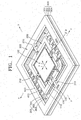
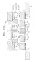
- a stage 100 having a mirror (not shown) formed on a surface thereof is supported by a first support portion including a first torsion bar 210 and a rectangular edge type movable frame 200, and the stage is capable of seesawing with respect to a center axis x-x in a first direction.
- the first support portion supporting the stage 100 is supported by a second support portion including a second torsion bar 310 and a rectangular edge type stationary frame 300, and the first support portion is capable of seesawing with respect to a center axis y-y in a second direction. Accordingly, the stage 100 is supported capable of moving in bi-axes directions by the first and second support portions.
- the stage 100 having the first direction x and the second direction y is connected to the rectangular edge type movable frame 200 by the two first torsion bars 210 and 210 extending to the first direction x .
- the stage 100 is supported capable of seesawing with respect to the center axis x-x in the first direction by the first torsion bars 210 and 210 located at both sides thereof.
- the rectangular edge type movable frame 200 has a first portions 200y parallel to the y-y axis and where the torsion bar 210 is connected to the middle portion thereof, and a second portion 200x parallel to the x-x axis and where the torsion bar 310 is connected to the middle portion thereof.
- the rectangular edge type stationary frame 300 is provided outside the rectangular edge type movable frame 200 to encompass the same and includes a first portion 300y extending in the first direction x and a second portion 300x extending in the second direction y .
- the stationary frame 300 and the movable frame 200 are connected to the second torsion bar 310 located at the middle portion between the respective second portions 200x and 300x.
- the second torsion bar 310 extends in the second direction y and thus the movable frame 200 is supported capable of seesawing with respect to the center axis y-y in the second direction.
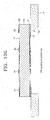
- the movable frame 200 and the stationary frame 300 have a multilayered structure having multiple layers 201, 202, and 203, and 301, 302, 303, and 304.
- the multilayered structure cannot be obtained from a single base material so that the stage 100, the movable frame 200, and the stationary frame 300 are formed from the multiple layers 201, 203, 301, 303, and 304 obtained from SI, SOI, and a glass substrate.
- Reference numerals 202 and 302 denote a bonding layer, in detail, eutectic bonding layer, to bond upper and lower multiple layers 201 and 203, and 301 and 303.
- the multilayered structure will be understood through a description about a method of manufacturing an actuator according to the present invention. As it will be described in the description of the manufacturing method, the bonding layer bonds an upper structure and a lower structure constituting an actuator. Thus, the upper structure and the lower structure are separately manufactured and incorporated in the final step.
- a stage driving portion generating the seesaw motion of the stage 100 is provided by a first driving comb electrode 120 formed on a lower surface of the stage 100 and a second stationary comb electrode 130 formed on a base 110 thereunder.
- FIG. 4 which is a section view taken along line y-y of FIG. 3, the first driving comb electrode 120 is arranged on a lower surface of the stage 100 at both sides with respect to the first torsion bar 210 which is a rotation axis of the stage 100 while the second stationary comb electrodes 130 is arranged on the base 110 corresponding to the first driving comb electrode 120.
- a movable frame driving portion making the stage 100 and the movable frame 200 seesaw with respect to a center axis in the y direction is provided between the movable frame 200 and the stationary frame 300.
- a second driving comb electrode 410 and a second stationary comb electrode 420 are alternately arranged at the side surfaces of the first portion 200y of the movable frame 200 and the first portion 300y of the stationary frame 300 facing the first portion 200y, respectively.
- the second driving comb electrode 410 and the second stationary comb electrode 420 are displaced deviating from each other in a third direction z perpendicular to a plane of the stage 100, that is, in a direction along which the movable frame 200 moves with respect to the second torsion bar 310.
- the displacement of the electrodes generates an electrostatic force therebetween in a third direction by an asymmetrical electric field in the third direction z between the electrodes.
- a seesaw type kinetic force of the movable frame 200 being coupled with the second driving comb electrode 410 and supported by the second torsion bar 310 is generated.
- the stage 100 can occupy the maximum area in the entire space.
- a second preferred embodiment 2 described below is related to an actuator where a plurality of stages are arranged in an array form.
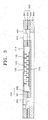
- FIG. 5 is a perspective view illustrating an actuator according to the present invention having an improved structure.
- FIG. 6 is a plan view of the actuator of FIG. 5.
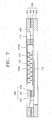
- FIG. 7 is a sectional view taken along line x-x of FIG. 6.
- a plurality of stages 100a where a mirror (not shown) is formed on a surface thereof are arranged in an array form and the stage array is encompassed by the rectangular edge type movable frame 200.
- a first torsion bar 21 0a constituting a first support portion with the rectangular edge type movable frame 200 is extended from both ends of each of the stages 100a.
- the stages 100a are supported by the first support portion capable of seesawing with respect to center axes x 0 - x 0 ,..., x n - x n parallel to the first direction, respectively.
- the first support portion supporting the stages 100a is supported by a second support portion including the second torsion bar 310 and the rectangular edge type stationary frame 300, capable of seesawing with respect to a center axis y-y in the second direction.
- the stages 100a are supported by the first and second support portions capable of moving in bi-axes directions.
- each of the stages 100a having the first directions x 0 - x n and the second direction y, parallel to one another, is connected to the rectangular edge type movable frame 200 by the two first torsion bars 210a extending in the first directions x 0 - x n .
- the stages 100a are supported by the first torsion bar 210a at both sides thereof capable of seesawing with respect to the center axes x 0 - x 0 ,..., x n - x n in the first direction.
- the rectangular edge type movable frame 200 supporting the stage array includes a first portion 200y extending parallel to the y-y axis and to which the first torsion bar 21 0a is connected and a second portion 200x extending parallel to the x-x axis and where the first torsion bar 210a is connected to the center thereof.
- the rectangular edge type movable frame 200 is encompassed by the rectangular edge type stationary frame 300 having a first portion 300y extending in the first direction and the second portion 300x extending in the second direction perpendicular to the first direction.
- the stationary frame 300 and the movable frame 200 are connected by the second torsion bar 310 disposed at the center portion between the respective second portions 200x and 300x.
- the second torsion bar 310 is extended in the second direction y so that the movable frame 200 can seesaw with respect to the center axis y-y in the second direction by the second torsion bar 310.
- the movable frame 200 and the stationary frame 300 have a multilayered structure of multiple layers 201, 202, and 203, and 301, 302, 303, and 304, respectively.
- the multilayered structure will be described later in detail in the description on a manufacturing method.
- a stage driving portion generating seesaw motions of the stages 100a includes the first driving comb electrode 120 formed on a lower surface of each of the stages 100a and the second stationary comb electrode 130 formed on the base 110 thereunder.
- the first driving comb electrode 120 is arranged on the lower surface of each of the stages 100a at both sides with respect to the first torsion bar 210a which is a rotation axis of each of the stages 100a.
- the second stationary comb electrode 130 corresponding to the first driving comb electrode 120 of the stages 100a is arranged on the base 110 in an array form.
- a movable frame driving portion making the stages 100a and the movable frame 200 supporting the stages 100a seesaw with respect to the center axis in the y direction is provided between the movable frame 200 and the stationary frame 300.
- the second driving comb electrode 410 and the second stationary comb electrode 420 are alternately arranged at side surfaces of the first portion 200y of the movable frame 200 and the firs portion 300y of the stationary frame 300, facing each other.
- the respective stages 100a seesawing with respect to the axis in the first direction can seesaw at the same time with respect to the axis in the second direction by the movable frame 200.
- the second driving comb electrode 410 and the second stationary comb electrode are displaced deviating from each other in the third direction z perpendicular to a plane of the stages 100a, that is, in a direction along which the movable frame 200 moves with respect to the second torsion bar 310.
- the displacement of the electrodes generates an electrostatic force therebetween in the third direction z by an asymmetrical electric field in the third direction (a direction of a seesaw motion of the stages) between the electrodes.
- a seesaw type kinetic force of the movable frame 200 supported by the second torsion bar 310 is generated.
- a sensing electrode having an opposed electrode structure like the stationary comb electrode and the driving comb electrode as a sort of sensor detecting a movement of the stages 100 and 100a from a change in electric capacitance, not providing a driving force to the stages 100 and 100a, can be selectively provided on the low surfaces of the stages 100 and 100a and the upper surfaces of the base corresponding thereto.
- the entire thickness of an optical scanner can be reduced compared to a structure in which an incident beam is reflected using a single stage, so that the weight of each stage can be remarkably reduced and a driving speed can be greatly increased.
- Electric wiring structures of the stages and electrodes are not described or shown in the first and second preferred embodiments and the drawings attached hereto. However, in these structures, a wiring layer for electric wiring from the outside and a through hole for electric connection between layers are present.
- An electric path is mainly provided by silicon and the silicon forms a body of the respective structure.
- the electric paths to the stages 100 and 100a are torsion bars 210 and 210a made of silicon and, in a portion needing electrical separation and insulation, silicon is patterned and an insulation material is filled in the appropriate portion.
- the through hole is filled with a conductive material for contact between layers through the through hole.
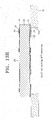
- FIG. 10 is a plan view illustrating an actuator according to the present invention for explaining an electric path of the actuator.
- a black portion 600 is an electric insulation layer or an insulation portion.
- Reference numerals P1, P2, P3, P4, and P5 are pads for wiring with an external circuit.
- the first pad P1 is provided at one side of the second portion 300x (at the upper side on the drawing) and connected to the second driving comb electrode 410 and the driving comb electrode 120 under the stage via the second torsion bar 310.
- the first pad P1 acts as a virtual ground.
- the second pads P2 and P3 are provided at the end sides of the first portion 300y of the stationary frame 300 electrically isolated by an insulation portion 602 in the stationary frame 300.
- the fourth pad P4 and the fifth pad P5 are provided at the second portion 300x at one side of the stationary frame 300 (in the lower portion on the drawing) and electrically separated from the first portion 300y.
- the fourth pad P4 and the fifth pad P5 are electrically separated by an insulation portion 601 crossing the second torsion bar 310 and connected to the movable frame 200 via the second torsion bar 310.
- the second portion 200x of the movable frame 200 where the fourth and fifth pads P4 and P5 are connected has a portion electrically separated by the insulation portion 601 at the center thereof and the insulation portion 603 at both end sides thereof.
- the portion where the fourth and fifth pads P4 and P5 are connected is connected by the first stationary comb electrodes 130 on the base 110 by the through hole and the conductive material filling the same.
- the insulation portion 600 crossing the second torsion bar 310 in the upper portion on the drawing is inserted not to electrically separate the second torsion bar 310 but to make the second torsion bar in the same shape as the insulation portion 601 in the lower portion of the drawing.
- a method of manufacturing an actuator according to a preferred embodiment of the present invention will be described below.
- a method of manufacturing the actuator according to the second preferred embodiment of the present invention will be described.
- the constituent elements shown in FIGS. 5 through 10 are cited with reference numerals, if necessary.
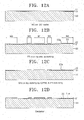
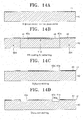
- a glass 10 is used as a material for a holder for fixing the actuator and a DFR (dry film resist) film 11 is coated on an upper surface of the Pyrex glass 10 and patterned.
- a window 11a to be opened has the size to be fixed when an edge portion of the stationary frame 300 of the actuator is put on the glass 10.
- the exposed portion of the glass 10 which is not covered by the window 11a is etched by sand blasting.
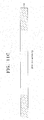
- FIG. 11C by removing the DFR film 11, a completed holder 10 having the window 10a of a predetermined pattern is obtained.
- an SOI (silicon on insulator) wafer having a thickness of about 500 ⁇ m and where an SiO 2 film 21 is formed between an upper silicon film 22 and a lower silicon main body 20 to be used as an etch stop layer when the first and second driving comb electrodes are formed.
- a photoresist mask 23 having a window of a predetermined pattern is formed on the silicon film 22.
- the portion covered by the mask 23 includes an area W1 where the stage 100a is to be formed, an area W2 where the movable frame 200 is to be formed, an area W3 where the stationary frame 300 is to be formed, and an area (not shown) where the torsion bar is to be formed.
- a portion on the silicon film 22 which is not covered by the photoresist mask 23 is etched in an ICPRIE (inductively coupled plasma reactive ion etching) method so that the insulation film (SiO 2 film) 21 is exposed through a window 23a of the photoresist mask 23. After etching is completed, the photoresist mask 23 is removed by stripping.
- ICPRIE inductively coupled plasma reactive ion etching
- an SiO 2 insulation film 21a is formed on the silicon film 22 and the exposed insulation film 21 in a thermal oxidation method.
- the silicon film 22 at the upper side is completely isolated from the outside by the insulation film 21 at the lower side and the insulation film 21a at the upper side.
- an silicon nitride (Si 3 N 4 ) film 24 is deposited on the insulation films 21 and 21a.
- a photoresist mask 25 having a window 25a is formed on the nitride film 24.
- the window 25a is a pattern to form a through hole for electric connection.
- the window 25a is formed to a predetermined size and in a predetermined number, on the stage area W1, the movable frame area W2, and the stationary frame area W3.
- the portion exposed through the window 25a is etched in a dry etching method so that a through hole 26 in an initial form in which the surface of the silicon film 22 is exposed at the bottom of the through hole 26.
- the silicon film 22 exposed at the bottom of the through hole 26 and the insulation film 21 thereunder are etched in an ICPRIE method.
- the photoresist mask 25 is removed.
- a conductive metal film for electric connection for example, an Au/Cr film 27, is deposited on the entire top surface of the resultant product.
- the Au/Cr film 27 on the portion which is not covered by the photoresist mask 28 is removed so that Au/Cr film 27 remains only on a necessary portion.
- the portion where the Au/Cr film 27 remains, that is, a portion covered by the photoresist mask 28, is a portion corresponding to the through hole 26 in the stage area W1 and the movable frame area W2 and a portion to be used as the through hole 26 and the pads P1, P2, P3, and P5 in the stationary area W3.
- the upper structure main body is installed on the holder 10 obtained from the above-described process.
- An anodic bonding is used herein and the bottom surface of the silicon main body 20 faces upward.
- a bottom surface 20a of the silicon main body 20 facing upward in a state in which the silicon main body 20 is installed on the holder 10 is grinded by a CMP (chemical mechanical polishing) method.
- an SiO 2 insulation film 29 is deposited on the bottom surface 20a.
- a photoresist mask 30 having a window 30a of a predetermined pattern is formed on the insulation film 29.
- the portion where the photoresist mask 30 remains corresponds to an area W4 where the first driving comb electrode 120 of the stage 100a is to be formed, an area W5 where the second driving comb electrode 410 is to be formed, and an area W6 where the stationary frame 300 is to be formed.
- the exposed portion of the insulation film 29 which is not covered by the photoresist mask 30 is removed in a dry etching method. Next, the photoresist mask 30 is removed.
- a photoresist mask 32 having a window 32a of a predetermined pattern is formed thereon.
- the Au/Cr seed layer 31 can be obtained by depositing Cr on the insulation film 29 to a thickness of about 500 Angstroms and Au thereon to a thickness of about 1500-2000 Angstroms.
- the window 32a is arranged corresponding to the through holes formed in the movable frame area W2 and the stationary frame area W3.
- a conductive metal film for example, an AuSn film 33
- AuSn film 33 is formed in an electroplating method on a surface of the seed layer exposed through the window 32a and the photoresist mask 32 is removed.
- the AuSn film 33 is used as an eutectic bonding layer when the main body of the upper structure is coupled to the lower structure.
- a photoresist mask 34 is formed on the AuSn film 33 by coating and patterning photoresist.
- the Au/Cr seed layer 31 which is not covered by the photoresist mask 34 is etched by wet etching.
- the first driving comb electrode 120 under the stage 100a (in the upper side of FIG. 131), the movable frame 200 encompassing the stage 100a, and the second driving comb electrode 410 and the stationary frame 300 formed at the outer side surface of the movable frame 200 are formed separated from the base material of the silicon main body 20.
- etching is stopped at the SiO 2 insulation film 21 in the SOI structure.
- the SiO 2 insulation film 21 and the Si 3 N 4 insulation film 24 remaining after the ICPRIE method is performed are penetrated so that the movable frame 200, the second driving comb electrode 410, and the stationary frame 300 are completely separated.
- the stage 100a and the movable frame 200 are connected by the first torsion bar 210 and the movable frame 200 and the stationary frame 300 are connected by the second torsion bar 310. Therefore, the upper structure applied to the actuator is completed.
- a reflection film 140 is formed by depositing a reflective material, for example, Au/Cr, on the upper surface of the stage 100a so that the upper structure is used as an optical scanner.
- a reflective material for example, Au/Cr
- the above-described steps are focused on the manufacture of a single device.
- the above device can be manufacture by a wafer unit process to obtain a plurality of devices with respect to a single wafer.
- An additional step may be accompanied during which the devices are collectively processed in the unit of a wafer.
- a dicing step to separate devices from the wafer is necessarily performed. Since the driving comb electrode may be damaged during the dicing step, a protective layer can be formed, prior to the dicing step, on the driving comb electrode to protect the driving comb electrode. After dicing is completed, the protective layer formed on the respective devices is finally removed.
- This additional step does not limit the scope of the present invention.
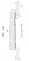
- a substrate 40 made of Pyrex glass and used as a support body of the lower structure in the actuator according to the present invention is prepared and an Si 3 N 4 insulation film 41 is formed on the surface of the substrate 40.
- a photoresist mask 42 having a window 42a of a predetermined pattern is formed on the Si 3 N 4 insulation film 41.
- the window 42a corresponds to a space between the movable frame 200 and the stationary frame 300 in the lower structure.
- the portion between the neighboring windows 42a is processed into the base 110 supporting the first stationary comb electrode 130 and the portions outside both windows 42a are processed into the lowermost multiple layer 304 of the stationary frame 300.
- the exposed portion of the Si 3 N 4 insulation film 41 which is not covered by the photoresist mask 42 is removed by dry etching.
- the exposed portion of the substrate 40 is etched by wet etching to form a well 40a having a predetermined depth.
- a silicon substrate 50 is prepared and a photoresist mask 51 having a window 51a of a predetermined pattern is formed on the surface of the silicon substrate 50.
- the window 51a is formed corresponding to portions to be removed such as a boundary area between the first stationary comb electrodes separated into two parts in the lower structure, a boundary area between the movable frame and the stationary frame, and a boundary area between the second stationary comb electrode and the movable frame in the stationary frame.
- the surface of the silicon substrate 50 which is not covered by the photoresist mask 51 is etched to a predetermined depth and the photoresist mask 51 is removed, so that an upper body of a semi-processed lower structure is obtained.
- processing surfaces of the upper and lower bodies of the lower structure are bonded by anodic bonding to face each other.
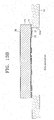
- a mask 60 is formed using a DFR film on one exposed side surface (the upper surface on the drawing) of the substrate 40 such as a glass substrate.
- the portion covered by the mask 60 is to be processed into the lowermost multiple layer 304 of the stationary frame 300.
- the glass substrate 40 is etched to a predetermined depth by sand blasting so that the base 110 in an initial form supporting the first stationary comb electrode and the lowermost multiple layer 304 of the stationary frame 300.
- the base 110 and the lowermost multiple layer 304 are connected by a temporary connection portion 111.
- the temporary connection portion 111 will be removed as the thickness of the base 110 decreases due to etching performed later.
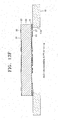
- the DFR mask 60 is removed and the outer surface (the upper surface on the drawing) of the substrate 50 is grinded by the CMP method.
- a photoresist mask 53 having a predetermined pattern is formed on the SiO 2 insulation film 52.
- the photoresist mask 53 has a pattern corresponding to the first stationary comb electrode on the base 110, the multiple layer 303 of the stationary frame 300, and the second stationary comb electrode 420 extending therefrom.
- the exposed portion of the SiO 2 insulation film 52 which is not covered by the photoresist mask 53 is etched and the photoresist mask 53 is removed.
- a photoresist mask 54 is formed on the SiO 2 insulation film 52 patterned in the above step.
- the photoresist mask 54 has a window 54a to etch the SiO 2 insulation film 52 and the silicon substrate 50 thereunder for physical and electric connection with the upper layer 301 of the stationary frame and the upper layer 201 of the movable frame obtained from the upper structure (refer to FIG. 16H).
- the silicon substrate 50 is etched to a predetermined depth by ICPRIE to form a well 50a corresponding to a give pattern.
- a photoresist sacrificial layer 55 is formed on the uppermost surface of the silicon substrate 50 except for the well 50a formed by etching in the preceding step.
- a portion which is not covered by the metal film 56 and the SiO 2 insulation film 52 is etched to form the first stationary comb electrode 130 and the second stationary comb electrode 420. All components except for the temporary connection portion 111 connecting the base 110 and the lower layer 304 of the stationary frame 300 in the lower structure are actually completed.
- the upper and lower structures completed by the above-described processes are aligned by an appropriate Assembling apparatus.
- the upper and lower structures are Assembled into one by eutectic bonding.
- a desired actuator is completed by removing the temporary connection portion 111 connecting the base 110 and the stationary frame 300.
- two vacuum chucks the upper portion of both frames of the upper structure is fixed by a vacuum chuck and the center portion of the lower structure is fixed by a vacuum chuck
- two structures are aligned while being observed through a microscope.
- two vacuum chucks are made to approach each other to assemble the two upper and lower structures into one.
- the metal eutectic bonding layer between the frames is melt to bond the upper and lower structures into one.
- the stationary comb electrode and the driving comb electrode for driving the stage are formed under the stage and the driving comb electrode and the stationary comb electrode overlap in a direction of driving the stage, an efficient arrangement of the driving comb electrodes for driving the stage is possible and a high speed driving is possible while a large are of a reflection surface is possible due to the arrangement. Also, the linear driving of a reflection surface is possible in the overall operation period. Furthermore, since the actuator according to the present invention has a structure of forming an asymmetrical electric field in a driving direction, an initial starting is possible without a starting electrode as in the conventional actuator and electric separation and control is available.
Landscapes
- Physics & Mathematics (AREA)
- General Physics & Mathematics (AREA)
- Optics & Photonics (AREA)
- Engineering & Computer Science (AREA)
- Computer Hardware Design (AREA)
- Microelectronics & Electronic Packaging (AREA)
- Micromachines (AREA)
- Mechanical Light Control Or Optical Switches (AREA)
- Mechanical Optical Scanning Systems (AREA)
- Design And Manufacture Of Integrated Circuits (AREA)
Applications Claiming Priority (2)
| Application Number | Priority Date | Filing Date | Title |
|---|---|---|---|
| KR10-2002-0063853A KR100486716B1 (ko) | 2002-10-18 | 2002-10-18 | 2-d 액튜에이터 및 그 제조방법 |
| KR2002063853 | 2002-10-18 |
Publications (3)
| Publication Number | Publication Date |
|---|---|
| EP1411024A2 true EP1411024A2 (de) | 2004-04-21 |
| EP1411024A3 EP1411024A3 (de) | 2005-11-16 |
| EP1411024B1 EP1411024B1 (de) | 2008-05-07 |
Family
ID=32041028
Family Applications (1)
| Application Number | Title | Priority Date | Filing Date |
|---|---|---|---|
| EP03255439A Expired - Lifetime EP1411024B1 (de) | 2002-10-18 | 2003-09-01 | 2-D Stellelement und dazugehöriges Herstellungsverfahren |
Country Status (7)
| Country | Link |
|---|---|
| US (1) | US6995495B2 (de) |
| EP (1) | EP1411024B1 (de) |
| JP (1) | JP2004139085A (de) |
| KR (1) | KR100486716B1 (de) |
| CN (1) | CN1214971C (de) |
| AT (1) | ATE394343T1 (de) |
| DE (1) | DE60320730D1 (de) |
Cited By (14)
| Publication number | Priority date | Publication date | Assignee | Title |
|---|---|---|---|---|
| WO2006098794A3 (en) * | 2005-03-09 | 2007-02-22 | Honeywell Int Inc | Mems device with thinned comb fingers |
| US7508111B2 (en) | 2004-10-19 | 2009-03-24 | Samsung Electronics Co., Ltd. | Biaxial actuators with comb electrodes having separated vertical positions |
| EP1875296A4 (de) * | 2005-04-22 | 2012-04-11 | Texas Instruments Inc | Nichtkontaktierende elektrostatisch gesteuerte mems-einrichtung |
| US8741682B2 (en) | 2006-05-18 | 2014-06-03 | Semiconductor Energy Laboratory Co., Ltd. | Microstructure, micromachine, and manufacturing method of microstructure and micromachine |
| WO2015109273A3 (en) * | 2014-01-19 | 2015-09-24 | Apple Inc. | Coupling schemes for gimbaled scanning mirror arrays |
| FR3021309A1 (fr) * | 2014-05-26 | 2015-11-27 | Commissariat Energie Atomique | Dispositif microelectronique et/ou nanoelectronique capacitif a compacite augmentee |
| WO2016085587A1 (en) * | 2014-11-24 | 2016-06-02 | Apple Inc. | Multi-mirror scanning depth engine |
| US9435638B2 (en) | 2012-03-22 | 2016-09-06 | Apple Inc. | Gimbaled scanning mirror array |
| US9523850B2 (en) | 2014-02-16 | 2016-12-20 | Apple Inc. | Beam scanning using an interference filter as a turning mirror |
| US9715107B2 (en) | 2012-03-22 | 2017-07-25 | Apple Inc. | Coupling schemes for gimbaled scanning mirror arrays |
| US9784838B1 (en) | 2014-11-26 | 2017-10-10 | Apple Inc. | Compact scanner with gimbaled optics |
| US9835853B1 (en) | 2014-11-26 | 2017-12-05 | Apple Inc. | MEMS scanner with mirrors of different sizes |
| FR3063992A1 (fr) * | 2017-03-16 | 2018-09-21 | Commissariat A L'energie Atomique Et Aux Energies Alternatives | Micro-dispositif comprenant au moins un element mobile |
| CN112973814A (zh) * | 2021-03-03 | 2021-06-18 | 北京理工大学 | 一种用于多层微流控芯片的层间自动对准键合装置及方法 |
Families Citing this family (65)
| Publication number | Priority date | Publication date | Assignee | Title |
|---|---|---|---|---|
| KR100486716B1 (ko) * | 2002-10-18 | 2005-05-03 | 삼성전자주식회사 | 2-d 액튜에이터 및 그 제조방법 |
| US7295726B1 (en) * | 2003-12-02 | 2007-11-13 | Adriatic Research Institute | Gimbal-less micro-electro-mechanical-system tip-tilt and tip-tilt-piston actuators and a method for forming the same |
| US7428353B1 (en) | 2003-12-02 | 2008-09-23 | Adriatic Research Institute | MEMS device control with filtered voltage signal shaping |
| EP1591824B1 (de) * | 2004-04-26 | 2012-05-09 | Panasonic Corporation | Microantrieb |
| KR100586967B1 (ko) * | 2004-05-28 | 2006-06-08 | 삼성전기주식회사 | 회전형 빗살 구동 액츄에이터 및 이를 이용한 가변 광감쇄기 |
| JP4385937B2 (ja) * | 2004-12-15 | 2009-12-16 | セイコーエプソン株式会社 | アクチュエータ |
| CN100419493C (zh) * | 2005-01-19 | 2008-09-17 | 鸿富锦精密工业(深圳)有限公司 | 光开关及其制作方法 |
| US7444740B1 (en) | 2005-01-31 | 2008-11-04 | Western Digital (Fremont), Llc | Damascene process for fabricating poles in recording heads |
| KR100707179B1 (ko) | 2005-02-07 | 2007-04-13 | 삼성전자주식회사 | 광스캐너 패키지 및 그 제조방법 |
| JP4427006B2 (ja) * | 2005-05-31 | 2010-03-03 | セイコーエプソン株式会社 | アクチュエータおよびその製造方法 |
| KR100647329B1 (ko) | 2005-07-09 | 2006-11-23 | 삼성전자주식회사 | 광스캐너 패키지 |
| KR100662463B1 (ko) | 2005-09-27 | 2007-01-02 | 엘지전자 주식회사 | 고속 정보 저장장치의 스캐너 및 그 제조방법 |
| JP4475421B2 (ja) * | 2005-12-28 | 2010-06-09 | 国立大学法人東北大学 | マイクロミラー、及び、マイクロミラーデバイス |
| JP4437320B2 (ja) * | 2006-01-06 | 2010-03-24 | 国立大学法人東北大学 | マイクロミラー、及び、マイクロミラーデバイス |
| JP4734122B2 (ja) * | 2006-01-16 | 2011-07-27 | 富士フイルム株式会社 | 光変調素子、アクチュエータ及びアクチュエータの駆動方法 |
| KR100682961B1 (ko) * | 2006-01-20 | 2007-02-15 | 삼성전자주식회사 | 회전형 마이크로 미러 |
| JP2007331095A (ja) * | 2006-05-18 | 2007-12-27 | Semiconductor Energy Lab Co Ltd | 微小構造体、マイクロマシンおよび半導体装置、ならびに微小構造体およびマイクロマシンの作製方法 |
| KR100790879B1 (ko) * | 2006-06-13 | 2008-01-03 | 삼성전자주식회사 | 맴스 디바이스의 콤전극 형성 방법 |
| JP5309441B2 (ja) * | 2006-11-16 | 2013-10-09 | 株式会社デンソー | 2次元光走査装置 |
| JP5103876B2 (ja) * | 2006-11-16 | 2012-12-19 | 株式会社デンソー | 2次元光走査装置 |
| WO2008090921A1 (ja) * | 2007-01-26 | 2008-07-31 | Panasonic Electric Works Co., Ltd. | 光走査ミラーと、半導体構造及びその製造方法 |
| JP4598795B2 (ja) * | 2007-03-30 | 2010-12-15 | 富士通株式会社 | マイクロ揺動素子およびマイクロ揺動素子アレイ |
| JP4542619B2 (ja) * | 2007-03-30 | 2010-09-15 | パイオニア株式会社 | 駆動装置 |
| WO2008126233A1 (ja) * | 2007-03-30 | 2008-10-23 | Pioneer Corporation | 駆動装置 |
| US8022597B2 (en) * | 2007-03-30 | 2011-09-20 | Pioneer Corporation | Driver |
| DE102007059856A1 (de) * | 2007-12-12 | 2009-06-18 | Robert Bosch Gmbh | Herstellungsverfahren für ein mikromechanisches Bauelement und mikromechaniches Bauelement |
| US7997742B2 (en) * | 2008-03-25 | 2011-08-16 | Microvision, Inc. | Capacitive comb feedback for high speed scan mirror |
| US8187902B2 (en) | 2008-07-09 | 2012-05-29 | The Charles Stark Draper Laboratory, Inc. | High performance sensors and methods for forming the same |
| US7924441B1 (en) | 2008-08-08 | 2011-04-12 | Mirrorcle Technologies, Inc. | Fast and high-precision 3D tracking and position measurement with MEMS micromirrors |
| JP4445027B2 (ja) * | 2008-09-04 | 2010-04-07 | 富士通株式会社 | マイクロミラー素子およびマイクロミラーアレイ |
| DE102009000168B4 (de) * | 2009-01-13 | 2017-03-23 | Robert Bosch Gmbh | Mikromechanische Strukturen und Verfahren zum Betrieb einer mikromechanischen Struktur |
| US8547619B2 (en) * | 2009-12-23 | 2013-10-01 | Jds Uniphase Corporation | Tiltable MEMS mirror |
| US9052567B2 (en) | 2010-11-15 | 2015-06-09 | DigitalOptics Corporation MEMS | Actuator inside of motion control |
| JP5736766B2 (ja) * | 2010-12-22 | 2015-06-17 | ミツミ電機株式会社 | 光走査装置 |
| JP5988592B2 (ja) * | 2012-01-19 | 2016-09-07 | キヤノン株式会社 | 可動ミラー、波面補正デバイスおよび眼底検査装置 |
| CN103145091B (zh) * | 2013-02-07 | 2015-05-06 | 东南大学 | 一种具有交错梳齿的静电驱动结构的制备方法 |
| KR101430123B1 (ko) * | 2013-10-11 | 2014-09-25 | 고려오트론(주) | 멤스 스캐너 |
| CN103744178A (zh) * | 2014-01-02 | 2014-04-23 | 桂林市光隆光电科技有限公司 | 一种可双轴旋转的mems微镜芯片 |
| US9428381B2 (en) * | 2014-03-03 | 2016-08-30 | Infineon Technologies Ag | Devices with thinned wafer |
| CN103901610B (zh) * | 2014-03-26 | 2016-12-07 | 重庆大学 | 百叶窗式mems大转角可调闪耀光栅光调制器及其阵列 |
| WO2015186772A1 (ja) * | 2014-06-05 | 2015-12-10 | 株式会社村田製作所 | Mems構造体 |
| US10948513B2 (en) * | 2014-10-20 | 2021-03-16 | Infineon Technologies Ag | Electronic device having a first electrode formed on a movable suspended mass opposing a second electrode formed on a cover layer |
| US9798135B2 (en) | 2015-02-16 | 2017-10-24 | Apple Inc. | Hybrid MEMS scanning module |
| DE102015204874A1 (de) * | 2015-03-18 | 2016-09-22 | Carl Zeiss Smt Gmbh | Einrichtung zur Verschwenkung eines Spiegel-Elements mit zwei Schwenk-Freiheitsgraden |
| US9897801B2 (en) | 2015-09-30 | 2018-02-20 | Apple Inc. | Multi-hinge mirror assembly |
| US9703096B2 (en) | 2015-09-30 | 2017-07-11 | Apple Inc. | Asymmetric MEMS mirror assembly |
| US10488652B2 (en) | 2016-09-21 | 2019-11-26 | Apple Inc. | Prism-based scanner |
| KR102773113B1 (ko) * | 2017-01-12 | 2025-02-25 | 삼성디스플레이 주식회사 | 증착용 마스크 어셈블리 |
| US10428475B2 (en) | 2017-06-12 | 2019-10-01 | Saris Cycling Group, Inc. | Collapsible lane delineator |
| JP6503149B1 (ja) | 2017-07-06 | 2019-04-17 | 浜松ホトニクス株式会社 | 光学デバイス及びその製造方法 |
| JP7112876B2 (ja) | 2017-07-06 | 2022-08-04 | 浜松ホトニクス株式会社 | 光学デバイス |
| TWI822686B (zh) | 2017-07-06 | 2023-11-21 | 日商濱松赫德尼古斯股份有限公司 | 光學裝置 |
| CN110799884B (zh) | 2017-07-06 | 2022-03-01 | 浜松光子学株式会社 | 光学装置 |
| TWI784023B (zh) | 2017-07-06 | 2022-11-21 | 日商濱松赫德尼古斯股份有限公司 | 光學裝置 |
| WO2019009397A1 (ja) | 2017-07-06 | 2019-01-10 | 浜松ホトニクス株式会社 | 光学デバイス |
| JP6514804B1 (ja) | 2017-07-06 | 2019-05-15 | 浜松ホトニクス株式会社 | 光学デバイス |
| EP3447560B1 (de) | 2017-08-23 | 2021-02-24 | Murata Manufacturing Co., Ltd. | Mems-reflektorsystem |
| CN115657297A (zh) | 2017-11-15 | 2023-01-31 | 浜松光子学株式会社 | 光学器件的制造方法 |
| US10870956B1 (en) | 2018-05-08 | 2020-12-22 | Studio5051, Llc | Traffic channelizer |
| JP6993951B2 (ja) * | 2018-10-15 | 2022-01-14 | 株式会社鷺宮製作所 | 振動発電素子 |
| CN114208006B (zh) | 2019-08-18 | 2024-10-29 | 苹果公司 | 具有电磁致动的力平衡微镜 |
| DE102020106474B4 (de) | 2019-08-30 | 2023-09-28 | Taiwan Semiconductor Manufacturing Co. Ltd. | Selbstgefluchtete dielektrische verkleidungsstruktur zum schutz in einem mems-kammaktuator |
| US11387748B2 (en) * | 2019-08-30 | 2022-07-12 | Taiwan Semiconductor Manufacturing Company, Ltd. | Self-aligned dielectric liner structure for protection in MEMS comb actuator |
| US12306303B2 (en) * | 2020-08-24 | 2025-05-20 | Beijing Voyager Technology Co., Ltd. | Mirror assembly for light steering |
| CN115893309B (zh) * | 2021-08-20 | 2026-03-24 | 华为技术有限公司 | 制造微机电系统梳齿结构的方法、系统和梳齿结构 |
Family Cites Families (22)
| Publication number | Priority date | Publication date | Assignee | Title |
|---|---|---|---|---|
| US4598585A (en) * | 1984-03-19 | 1986-07-08 | The Charles Stark Draper Laboratory, Inc. | Planar inertial sensor |
| US5025346A (en) | 1989-02-17 | 1991-06-18 | Regents Of The University Of California | Laterally driven resonant microstructures |
| JPH0554782A (ja) * | 1991-08-28 | 1993-03-05 | Sharp Corp | マイクロマシーン |
| JPH10253912A (ja) * | 1997-01-13 | 1998-09-25 | Denso Corp | 光走査装置 |
| JP3011144B2 (ja) * | 1997-07-31 | 2000-02-21 | 日本電気株式会社 | 光スキャナとその駆動方法 |
| JP4072743B2 (ja) * | 1998-11-13 | 2008-04-09 | 日本ビクター株式会社 | 光偏向器及びこれを用いた表示装置 |
| US6753638B2 (en) * | 2000-02-03 | 2004-06-22 | Calient Networks, Inc. | Electrostatic actuator for micromechanical systems |
| US6330102B1 (en) * | 2000-03-24 | 2001-12-11 | Onix Microsystems | Apparatus and method for 2-dimensional steered-beam NxM optical switch using single-axis mirror arrays and relay optics |
| TW505614B (en) * | 2000-06-09 | 2002-10-11 | Speed Corp C | Optical mirror system with multi-axis rotational control |
| KR100474835B1 (ko) * | 2000-07-18 | 2005-03-08 | 삼성전자주식회사 | 다축 구동을 위한 싱글스테이지 마이크로구동기 |
| KR100400218B1 (ko) * | 2000-08-18 | 2003-10-30 | 삼성전자주식회사 | 마이크로 액튜에이터 및 그 제조방법 |
| JP2002148554A (ja) * | 2000-11-03 | 2002-05-22 | Samsung Electronics Co Ltd | 光スキャナ及びこれを適用したレーザ映像投射装置並びにその駆動方法 |
| US20020136485A1 (en) * | 2001-02-02 | 2002-09-26 | Reed Jason D. | Apparatus and method for micro-electromechanical systems two-dimensional large movement electrostatic comb drive |
| JP4102037B2 (ja) * | 2001-04-26 | 2008-06-18 | 富士通株式会社 | マイクロミラー素子およびその製造方法 |
| KR100434541B1 (ko) * | 2001-08-24 | 2004-06-05 | 삼성전자주식회사 | 광스캐너 및 그 제조방법 |
| KR100447214B1 (ko) * | 2002-02-08 | 2004-09-04 | 엘지전자 주식회사 | 마이크로 미러 |
| JP4140816B2 (ja) * | 2002-05-24 | 2008-08-27 | 富士通株式会社 | マイクロミラー素子 |
| JP3987382B2 (ja) * | 2002-06-11 | 2007-10-10 | 富士通株式会社 | マイクロミラー素子およびその製造方法 |
| JP3793125B2 (ja) * | 2002-07-18 | 2006-07-05 | 富士通株式会社 | デバイスチップの製造方法 |
| KR100469062B1 (ko) * | 2002-08-13 | 2005-02-02 | 한국전자통신연구원 | 광통신용 주사 미세거울 및 그 제조 방법 |
| KR100486716B1 (ko) * | 2002-10-18 | 2005-05-03 | 삼성전자주식회사 | 2-d 액튜에이터 및 그 제조방법 |
| KR100940206B1 (ko) * | 2003-10-24 | 2010-02-10 | 삼성전자주식회사 | 주파수 변조 가능한 공진형 스캐너 |
-
2002
- 2002-10-18 KR KR10-2002-0063853A patent/KR100486716B1/ko not_active Expired - Fee Related
-
2003
- 2003-09-01 DE DE60320730T patent/DE60320730D1/de not_active Expired - Fee Related
- 2003-09-01 EP EP03255439A patent/EP1411024B1/de not_active Expired - Lifetime
- 2003-09-01 AT AT03255439T patent/ATE394343T1/de not_active IP Right Cessation
- 2003-09-02 CN CNB031556809A patent/CN1214971C/zh not_active Expired - Fee Related
- 2003-10-16 US US10/685,800 patent/US6995495B2/en not_active Expired - Fee Related
- 2003-10-20 JP JP2003358849A patent/JP2004139085A/ja active Pending
Cited By (21)
| Publication number | Priority date | Publication date | Assignee | Title |
|---|---|---|---|---|
| US7508111B2 (en) | 2004-10-19 | 2009-03-24 | Samsung Electronics Co., Ltd. | Biaxial actuators with comb electrodes having separated vertical positions |
| EP1659437A3 (de) * | 2004-10-19 | 2009-06-17 | Samsung Electronics Co., Ltd. | Zweiachsige Positioniereinrichtung und Verfahren zur Herstellung |
| WO2006098794A3 (en) * | 2005-03-09 | 2007-02-22 | Honeywell Int Inc | Mems device with thinned comb fingers |
| US7258010B2 (en) | 2005-03-09 | 2007-08-21 | Honeywell International Inc. | MEMS device with thinned comb fingers |
| EP1875296A4 (de) * | 2005-04-22 | 2012-04-11 | Texas Instruments Inc | Nichtkontaktierende elektrostatisch gesteuerte mems-einrichtung |
| US8741682B2 (en) | 2006-05-18 | 2014-06-03 | Semiconductor Energy Laboratory Co., Ltd. | Microstructure, micromachine, and manufacturing method of microstructure and micromachine |
| US9130012B2 (en) | 2006-05-18 | 2015-09-08 | Semiconductor Energy Laboratory Co., Ltd. | Microstructure, micromachine, and manufacturing method of microstructure and micromachine |
| US9435638B2 (en) | 2012-03-22 | 2016-09-06 | Apple Inc. | Gimbaled scanning mirror array |
| US9715107B2 (en) | 2012-03-22 | 2017-07-25 | Apple Inc. | Coupling schemes for gimbaled scanning mirror arrays |
| WO2015109273A3 (en) * | 2014-01-19 | 2015-09-24 | Apple Inc. | Coupling schemes for gimbaled scanning mirror arrays |
| US9523850B2 (en) | 2014-02-16 | 2016-12-20 | Apple Inc. | Beam scanning using an interference filter as a turning mirror |
| FR3021309A1 (fr) * | 2014-05-26 | 2015-11-27 | Commissariat Energie Atomique | Dispositif microelectronique et/ou nanoelectronique capacitif a compacite augmentee |
| US9631952B2 (en) | 2014-05-26 | 2017-04-25 | Commissariat à l'énergie atomique et aux énergies alternatives | Capacitive microelectronic and/or nanoelectronic device with increased compactness |
| WO2016085587A1 (en) * | 2014-11-24 | 2016-06-02 | Apple Inc. | Multi-mirror scanning depth engine |
| US9784838B1 (en) | 2014-11-26 | 2017-10-10 | Apple Inc. | Compact scanner with gimbaled optics |
| US9835853B1 (en) | 2014-11-26 | 2017-12-05 | Apple Inc. | MEMS scanner with mirrors of different sizes |
| FR3063992A1 (fr) * | 2017-03-16 | 2018-09-21 | Commissariat A L'energie Atomique Et Aux Energies Alternatives | Micro-dispositif comprenant au moins un element mobile |
| CN110650916A (zh) * | 2017-03-16 | 2020-01-03 | 赛峰集团 | 包括至少两个可移动元件的微器件 |
| US11312618B2 (en) | 2017-03-16 | 2022-04-26 | Commissariat À L'Énergie Atomique Et Aux Énergies Alternatives Safran | Microdevice comprising at least two movable elements |
| CN112973814A (zh) * | 2021-03-03 | 2021-06-18 | 北京理工大学 | 一种用于多层微流控芯片的层间自动对准键合装置及方法 |
| CN112973814B (zh) * | 2021-03-03 | 2022-03-18 | 北京理工大学 | 一种用于多层微流控芯片的层间自动对准键合装置及方法 |
Also Published As
| Publication number | Publication date |
|---|---|
| KR100486716B1 (ko) | 2005-05-03 |
| KR20040035116A (ko) | 2004-04-29 |
| CN1490240A (zh) | 2004-04-21 |
| EP1411024A3 (de) | 2005-11-16 |
| US20040081391A1 (en) | 2004-04-29 |
| DE60320730D1 (de) | 2008-06-19 |
| ATE394343T1 (de) | 2008-05-15 |
| JP2004139085A (ja) | 2004-05-13 |
| EP1411024B1 (de) | 2008-05-07 |
| US6995495B2 (en) | 2006-02-07 |
| CN1214971C (zh) | 2005-08-17 |
Similar Documents
| Publication | Publication Date | Title |
|---|---|---|
| EP1411024B1 (de) | 2-D Stellelement und dazugehöriges Herstellungsverfahren | |
| EP1288696B1 (de) | Optischer Scanner und Herstellungsverfahren dafür | |
| US7329930B2 (en) | Micromechanical actuator with multiple-plane comb electrodes and methods of making | |
| KR101659638B1 (ko) | 층상형 mems 구조 및 그 방법 | |
| US7508111B2 (en) | Biaxial actuators with comb electrodes having separated vertical positions | |
| EP1180493B1 (de) | Mikroaktor und dessen Herstellungsverfahren | |
| US7005775B2 (en) | Microfabricated torsional drive utilizing lateral electrostatic force | |
| CN110031966B (zh) | 一种微镜及其制造方法 | |
| US7813028B2 (en) | Manufacturing method for stress compensated X-Y gimbaled MEMS mirror array | |
| US7203393B2 (en) | MEMS micro mirrors driven by electrodes fabricated on another substrate | |
| Hah et al. | A self-aligned vertical comb-drive actuator on an SOI wafer for a 2D scanning micromirror | |
| US20230023348A1 (en) | Fabrication of a micro-mirror with reduced moment of inertia and mems devices | |
| KR100404195B1 (ko) | 마이크로 미러 및 그 제조방법 | |
| HK1161362A (en) | Mems device |
Legal Events
| Date | Code | Title | Description |
|---|---|---|---|
| PUAI | Public reference made under article 153(3) epc to a published international application that has entered the european phase |
Free format text: ORIGINAL CODE: 0009012 |
|
| AK | Designated contracting states |
Kind code of ref document: A2 Designated state(s): AT BE BG CH CY CZ DE DK EE ES FI FR GB GR HU IE IT LI LU MC NL PT RO SE SI SK TR |
|
| AX | Request for extension of the european patent |
Extension state: AL LT LV MK |
|
| PUAL | Search report despatched |
Free format text: ORIGINAL CODE: 0009013 |
|
| AK | Designated contracting states |
Kind code of ref document: A3 Designated state(s): AT BE BG CH CY CZ DE DK EE ES FI FR GB GR HU IE IT LI LU MC NL PT RO SE SI SK TR |
|
| AX | Request for extension of the european patent |
Extension state: AL LT LV MK |
|
| RIC1 | Information provided on ipc code assigned before grant |
Ipc: 7G 02B 26/08 B Ipc: 7B 81B 3/00 A |
|
| 17P | Request for examination filed |
Effective date: 20060125 |
|
| AKX | Designation fees paid |
Designated state(s): AT BE BG CH CY CZ DE DK EE ES FI FR GB GR HU IE IT LI LU MC NL PT RO SE SI SK TR |
|
| 17Q | First examination report despatched |
Effective date: 20060706 |
|
| GRAP | Despatch of communication of intention to grant a patent |
Free format text: ORIGINAL CODE: EPIDOSNIGR1 |
|
| GRAS | Grant fee paid |
Free format text: ORIGINAL CODE: EPIDOSNIGR3 |
|
| GRAA | (expected) grant |
Free format text: ORIGINAL CODE: 0009210 |
|
| AK | Designated contracting states |
Kind code of ref document: B1 Designated state(s): AT BE BG CH CY CZ DE DK EE ES FI FR GB GR HU IE IT LI LU MC NL PT RO SE SI SK TR |
|
| REG | Reference to a national code |
Ref country code: GB Ref legal event code: FG4D |
|
| RIN1 | Information on inventor provided before grant (corrected) |
Inventor name: LEE, JIN-HO Inventor name: KO, YOUNG-CHUL |
|
| REG | Reference to a national code |
Ref country code: CH Ref legal event code: EP |
|
| REG | Reference to a national code |
Ref country code: IE Ref legal event code: FG4D Free format text: LANGUAGE OF EP DOCUMENT: FRENCH |
|
| REF | Corresponds to: |
Ref document number: 60320730 Country of ref document: DE Date of ref document: 20080619 Kind code of ref document: P |
|
| PG25 | Lapsed in a contracting state [announced via postgrant information from national office to epo] |
Ref country code: SI Free format text: LAPSE BECAUSE OF FAILURE TO SUBMIT A TRANSLATION OF THE DESCRIPTION OR TO PAY THE FEE WITHIN THE PRESCRIBED TIME-LIMIT Effective date: 20080507 |
|
| PG25 | Lapsed in a contracting state [announced via postgrant information from national office to epo] |
Ref country code: ES Free format text: LAPSE BECAUSE OF FAILURE TO SUBMIT A TRANSLATION OF THE DESCRIPTION OR TO PAY THE FEE WITHIN THE PRESCRIBED TIME-LIMIT Effective date: 20080818 Ref country code: FI Free format text: LAPSE BECAUSE OF FAILURE TO SUBMIT A TRANSLATION OF THE DESCRIPTION OR TO PAY THE FEE WITHIN THE PRESCRIBED TIME-LIMIT Effective date: 20080507 Ref country code: NL Free format text: LAPSE BECAUSE OF FAILURE TO SUBMIT A TRANSLATION OF THE DESCRIPTION OR TO PAY THE FEE WITHIN THE PRESCRIBED TIME-LIMIT Effective date: 20080507 |
|
| NLV1 | Nl: lapsed or annulled due to failure to fulfill the requirements of art. 29p and 29m of the patents act | ||
| PG25 | Lapsed in a contracting state [announced via postgrant information from national office to epo] |
Ref country code: AT Free format text: LAPSE BECAUSE OF FAILURE TO SUBMIT A TRANSLATION OF THE DESCRIPTION OR TO PAY THE FEE WITHIN THE PRESCRIBED TIME-LIMIT Effective date: 20080507 |
|
| PGFP | Annual fee paid to national office [announced via postgrant information from national office to epo] |
Ref country code: FR Payment date: 20080915 Year of fee payment: 6 |
|
| PGFP | Annual fee paid to national office [announced via postgrant information from national office to epo] |
Ref country code: GB Payment date: 20080903 Year of fee payment: 6 |
|
| PG25 | Lapsed in a contracting state [announced via postgrant information from national office to epo] |
Ref country code: PT Free format text: LAPSE BECAUSE OF FAILURE TO SUBMIT A TRANSLATION OF THE DESCRIPTION OR TO PAY THE FEE WITHIN THE PRESCRIBED TIME-LIMIT Effective date: 20081007 Ref country code: DK Free format text: LAPSE BECAUSE OF FAILURE TO SUBMIT A TRANSLATION OF THE DESCRIPTION OR TO PAY THE FEE WITHIN THE PRESCRIBED TIME-LIMIT Effective date: 20080507 Ref country code: CZ Free format text: LAPSE BECAUSE OF FAILURE TO SUBMIT A TRANSLATION OF THE DESCRIPTION OR TO PAY THE FEE WITHIN THE PRESCRIBED TIME-LIMIT Effective date: 20080507 Ref country code: SE Free format text: LAPSE BECAUSE OF FAILURE TO SUBMIT A TRANSLATION OF THE DESCRIPTION OR TO PAY THE FEE WITHIN THE PRESCRIBED TIME-LIMIT Effective date: 20080807 |
|
| PGFP | Annual fee paid to national office [announced via postgrant information from national office to epo] |
Ref country code: DE Payment date: 20080912 Year of fee payment: 6 |
|
| PG25 | Lapsed in a contracting state [announced via postgrant information from national office to epo] |
Ref country code: BE Free format text: LAPSE BECAUSE OF FAILURE TO SUBMIT A TRANSLATION OF THE DESCRIPTION OR TO PAY THE FEE WITHIN THE PRESCRIBED TIME-LIMIT Effective date: 20080507 Ref country code: SK Free format text: LAPSE BECAUSE OF FAILURE TO SUBMIT A TRANSLATION OF THE DESCRIPTION OR TO PAY THE FEE WITHIN THE PRESCRIBED TIME-LIMIT Effective date: 20080507 Ref country code: RO Free format text: LAPSE BECAUSE OF FAILURE TO SUBMIT A TRANSLATION OF THE DESCRIPTION OR TO PAY THE FEE WITHIN THE PRESCRIBED TIME-LIMIT Effective date: 20080507 |
|
| PLBE | No opposition filed within time limit |
Free format text: ORIGINAL CODE: 0009261 |
|
| STAA | Information on the status of an ep patent application or granted ep patent |
Free format text: STATUS: NO OPPOSITION FILED WITHIN TIME LIMIT |
|
| 26N | No opposition filed |
Effective date: 20090210 |
|
| PG25 | Lapsed in a contracting state [announced via postgrant information from national office to epo] |
Ref country code: EE Free format text: LAPSE BECAUSE OF FAILURE TO SUBMIT A TRANSLATION OF THE DESCRIPTION OR TO PAY THE FEE WITHIN THE PRESCRIBED TIME-LIMIT Effective date: 20080507 Ref country code: MC Free format text: LAPSE BECAUSE OF NON-PAYMENT OF DUE FEES Effective date: 20080930 Ref country code: BG Free format text: LAPSE BECAUSE OF FAILURE TO SUBMIT A TRANSLATION OF THE DESCRIPTION OR TO PAY THE FEE WITHIN THE PRESCRIBED TIME-LIMIT Effective date: 20080807 |
|
| REG | Reference to a national code |
Ref country code: CH Ref legal event code: PL |
|
| PG25 | Lapsed in a contracting state [announced via postgrant information from national office to epo] |
Ref country code: IE Free format text: LAPSE BECAUSE OF NON-PAYMENT OF DUE FEES Effective date: 20080901 |
|
| PG25 | Lapsed in a contracting state [announced via postgrant information from national office to epo] |
Ref country code: IT Free format text: LAPSE BECAUSE OF FAILURE TO SUBMIT A TRANSLATION OF THE DESCRIPTION OR TO PAY THE FEE WITHIN THE PRESCRIBED TIME-LIMIT Effective date: 20080507 |
|
| PG25 | Lapsed in a contracting state [announced via postgrant information from national office to epo] |
Ref country code: CH Free format text: LAPSE BECAUSE OF NON-PAYMENT OF DUE FEES Effective date: 20080930 Ref country code: LI Free format text: LAPSE BECAUSE OF NON-PAYMENT OF DUE FEES Effective date: 20080930 |
|
| GBPC | Gb: european patent ceased through non-payment of renewal fee |
Effective date: 20090901 |
|
| REG | Reference to a national code |
Ref country code: FR Ref legal event code: ST Effective date: 20100531 |
|
| PG25 | Lapsed in a contracting state [announced via postgrant information from national office to epo] |
Ref country code: LU Free format text: LAPSE BECAUSE OF NON-PAYMENT OF DUE FEES Effective date: 20080901 Ref country code: HU Free format text: LAPSE BECAUSE OF FAILURE TO SUBMIT A TRANSLATION OF THE DESCRIPTION OR TO PAY THE FEE WITHIN THE PRESCRIBED TIME-LIMIT Effective date: 20081108 Ref country code: FR Free format text: LAPSE BECAUSE OF NON-PAYMENT OF DUE FEES Effective date: 20090930 Ref country code: DE Free format text: LAPSE BECAUSE OF NON-PAYMENT OF DUE FEES Effective date: 20100401 Ref country code: CY Free format text: LAPSE BECAUSE OF FAILURE TO SUBMIT A TRANSLATION OF THE DESCRIPTION OR TO PAY THE FEE WITHIN THE PRESCRIBED TIME-LIMIT Effective date: 20080507 |
|
| PG25 | Lapsed in a contracting state [announced via postgrant information from national office to epo] |
Ref country code: TR Free format text: LAPSE BECAUSE OF FAILURE TO SUBMIT A TRANSLATION OF THE DESCRIPTION OR TO PAY THE FEE WITHIN THE PRESCRIBED TIME-LIMIT Effective date: 20080507 |
|
| PG25 | Lapsed in a contracting state [announced via postgrant information from national office to epo] |
Ref country code: GR Free format text: LAPSE BECAUSE OF FAILURE TO SUBMIT A TRANSLATION OF THE DESCRIPTION OR TO PAY THE FEE WITHIN THE PRESCRIBED TIME-LIMIT Effective date: 20080808 |
|
| PG25 | Lapsed in a contracting state [announced via postgrant information from national office to epo] |
Ref country code: GB Free format text: LAPSE BECAUSE OF NON-PAYMENT OF DUE FEES Effective date: 20090901 |