EP1416430A2 - Anordnung zum Drucken eines Druckbildes mit Bereichen unterschiedlicher Druckbildauflösung - Google Patents
Anordnung zum Drucken eines Druckbildes mit Bereichen unterschiedlicher Druckbildauflösung Download PDFInfo
- Publication number
- EP1416430A2 EP1416430A2 EP03090190A EP03090190A EP1416430A2 EP 1416430 A2 EP1416430 A2 EP 1416430A2 EP 03090190 A EP03090190 A EP 03090190A EP 03090190 A EP03090190 A EP 03090190A EP 1416430 A2 EP1416430 A2 EP 1416430A2
- Authority
- EP
- European Patent Office
- Prior art keywords
- value
- signal
- address
- data
- pixel data
- Prior art date
- Legal status (The legal status is an assumption and is not a legal conclusion. Google has not performed a legal analysis and makes no representation as to the accuracy of the status listed.)
- Granted
Links
Images





Classifications
-
- G—PHYSICS
- G06—COMPUTING OR CALCULATING; COUNTING
- G06K—GRAPHICAL DATA READING; PRESENTATION OF DATA; RECORD CARRIERS; HANDLING RECORD CARRIERS
- G06K15/00—Arrangements for producing a permanent visual presentation of the output data, e.g. computer output printers
- G06K15/02—Arrangements for producing a permanent visual presentation of the output data, e.g. computer output printers using printers
-
- G—PHYSICS
- G07—CHECKING-DEVICES
- G07B—TICKET-ISSUING APPARATUS; FARE-REGISTERING APPARATUS; FRANKING APPARATUS
- G07B17/00—Franking apparatus
- G07B17/00459—Details relating to mailpieces in a franking system
- G07B17/00508—Printing or attaching on mailpieces
-
- G—PHYSICS
- G06—COMPUTING OR CALCULATING; COUNTING
- G06K—GRAPHICAL DATA READING; PRESENTATION OF DATA; RECORD CARRIERS; HANDLING RECORD CARRIERS
- G06K2215/00—Arrangements for producing a permanent visual presentation of the output data
- G06K2215/0082—Architecture adapted for a particular function
-
- G—PHYSICS
- G07—CHECKING-DEVICES
- G07B—TICKET-ISSUING APPARATUS; FARE-REGISTERING APPARATUS; FRANKING APPARATUS
- G07B17/00—Franking apparatus
- G07B17/00459—Details relating to mailpieces in a franking system
- G07B17/00508—Printing or attaching on mailpieces
- G07B2017/00637—Special printing techniques, e.g. interlacing
Definitions
- the invention relates to an arrangement for printing a print image Areas of different print image resolution, according to the generic term of claim 1.
- the invention comes in franking machines, Addressing machines and other printing mail processing equipment for use.
- the machine also enables T1000, business cards, fee and
- Print out court cost stamp images i.e. To generate print images, which differ significantly in structure and content from a franking stamp image distinguish, but have the same print resolution.
- a franking stamp image usually comprises a postage stamp image, a Postmark image with the post office and date as well as the aforementioned advertising stamp image and will be in the order mentioned generated, for example, by the franking machine T1000, by a Printing of printing columns in a vertical arrangement to the franking material transport direction. The entire print column is made by a single Thermal transfer print head prints.
- the machine can do one maximum throughput of franking goods of 2200 letters / hour at one Print resolution 240 dot per 30 mm, i.e. Reach 203 dpi, however Manual franking limits the practically achievable Throughput of franking goods.
- EP 578 042 B1 (US 5,608,636) describes a method for controlling the column-wise printing of a postage stamp known in the coded Image information before the respective printing process in binary signals for Controlling printing elements are implemented, the implemented changeable and unchangeable image data only during the Printing.
- the latter includes a message with a postal information including postage data for transportation of the letter.
- Modern franking machines enable a so-called Security imprint, i.e. an impression of a special marking in addition to the aforementioned notice. For example a message authentication code or generates a signature and then a string or a barcode as Mark formed. If a security imprint with one Marking is printed, this enables a verification of the authenticity the security imprint, for example in the post office or private carrier (US 5,953,426, US 6,041,704).
- the modules each only have one row of nozzles with 64 nozzles and so far for the pressure column are arranged obliquely so that each row of nozzles is pointed Angle to the direction of transport of the franking good.
- EP 921 008 A1 and EP 921 009 A1 A method and an arrangement for tolerance compensation have already been made proposed in EP 921 008 A1 and EP 921 009 A1, wherein individual printhead data in a non-volatile memory of the printhead are stored and taken into account in the pressure pulse delay become.
- the pixel offset error goes beyond the size of that a printing column is spaced from the next, the binary pixel data in the pixel memory can be changed.
- a solution for printing image formation known from US 5,707,158 and EP 762 334 B1 for the Jetmail® describes how a complete print image descriptive data generated before printing and stored and goes from a control file for field-by-field generation of the Print image in a pixel memory before printing.
- the print image is defined in sub-image files of the control file and is in pixel files as Pattern saved. So that the printing device directly on the pixel data binary pixel data cannot be accessed in order a print image column, but each along a diagonal in three superimposed sections as a changed pattern in one Pixel memory saved to that when printing due to the noninterlaced arrangement of the modules caused changes in the pattern compensate.
- the solution is based on complete with the participation of one Pixel data changing unit changed patterns of binary pixel data, which are buffered in the pixel memory, the print images Before printing, be put together so that the latter by a Print data control directly from the pixel memory into a shift register read in, transferred serially to a shift register in the printhead and can be included in a latch.
- the print data control is implemented in an ASIC together with other modules (US 5,710,721, EP 1 154 382 A2).
- variable picture elements between successive frankings can change so that it is in the form of binary pixel data in a pixel memory saved before printing.
- the one for printing required arrangement of the pixels in the pixel memory is on Because of the inclination of the print modules of a print head for the Changing the picture elements by the microprocessor inconvenient and would require a lot of computation. Through the latter, too with the support of a pixel processing unit only a small one Number of variable picture elements between the prints can be changed.
- variable and fixed image data elements are in a non-volatile Memory, where a part of the fixed image data elements is compressed.
- the print image data is only for printing each print column immediately before printing them from changeable and unchangeable Composed image data, i.e. the image data for an impression are not in binary form in a memory area, but in a with comparable to the method disclosed in EP 578 042 B1 for T1000 Shape.
- variable image data elements are controlled by a controller identified in the non-volatile memory and data associated with the variable image data elements correspond to another controller passed to download the variable and fixed image data elements, connect to each other and then print.
- the proposed one Control requires one for each variable image data element variable address register. The number of variable picture elements is thus limited by the number of address registers.
- a postage 1 ⁇ 2 inch inkjet printhead comes in some franking machines today with bubble-jet technology used in a cartridge arranged, for example, of the HP 51640 type from Hewlett Packard and is secured by special means (EP 1 132 868 A1).
- 1 ⁇ 2 inch Inkjet printhead 300 nozzles are arranged in two rows of nozzles, which are used for Franking material transport direction orthogonal and to each other in the print image column direction and arranged offset in the franking material transport direction are ("interlaced" principle).
- the machine can achieve a high throughput of franking goods (5500 letters each Hour).
- the amount of print image data between two impressions needs to be changed is not only very high but also needs to be changed can be provided in a shorter time.
- the print image will be in the Pixel storage as a correspondingly modified pattern of binary Pixel data mapped. This will change the picture elements by the microprocessor again complicated and requires a lot of computing, which either only with an expensive microprocessor in the required time can be provided or the throughput Franking is reduced accordingly.
- the object of the invention is an economical solution a control of printing a printed image with areas different Print image resolution on moving mail in a mail processing device with high-resolution print heads for a high To create throughput of mail.
- a microprocessor responsible for a complete mail processing system be relieved.
- the inventive solution assumes that the used Inkjet printheads place high demands on the print resolution fulfill.
- the print resolution orthogonal to the transport direction of a mail item the printed image column can have a maximum value (600 dpi) to reach.
- the mail processing device is, for example, a franking machine whose franking stamp image is a printed image with a predetermined one Number of print image columns is approximately one inch in length.
- a commercially available inkjet printhead with a half-inch width only a part of the Print image (print field) can be used for printing the two half-inch inkjet printheads.
- Print image there is an image in the form of a pattern of binary pixel data.
- the pixel data for two complete print fields are under Use of data from a read-only memory by the microprocessor generated and stored in the pixel memory in the form of data words.
- the number in a data string corresponds to the maximum possible Print resolution of the print head.
- the saved in the pixel memory binary pixel data are transmitted for print data control and grouped according to the type of printhead during printing. However, the printed image can also contain sections that are not high-resolution must be printed out. Because a pattern with a variety reflects the print image of data strings arranged in columns, there is a reflection of a compressed printed image section, when the binary pixel data is compressed into data words one Data strings are saved. That is the length of the corresponding one Data strings is reduced, contributes to a considerable saving of storage space in the pixel memory at. Through the print data control when the pixel data is decompressed, the missing pixel data is generated.
- pixel data be easily changed before printing and binary form are stored word by word in the pixel memory and that a switchable number of data words for printing of sections in the printed image with a changed resolution are and that the print data control depending on the changed Print image resolution is designed to be switchable accordingly.
- the print data controller has means for generating a print image in Depends on the required resolution and thus relieves the microprocessor used in the mail processing device, on the one hand for the change in the print data of the variable print image elements in the Pixel memory between the frankings. Then or in parallel For this purpose, print data is processed via direct memory access (DMA) for print data control transferred.
- DMA direct memory access
- Two pixel data preparation units are identified by one special controller driven to get binary pixel data from the pixel memory to transfer to a buffer and around bitwise binary To select pixel data which are stored in a collective register of the respective Pixel data processing inscribed and then in a shift register are taken over, so that the pixel data in such a special order can be supplied by the shift register like that when printing print columns with both postal 1 ⁇ 2 inch inkjet print heads is needed.
- the microprocessor is programmed, one Number of data strings with a switchable number of data words to save in pixel memory.
- the print data control is by means equipped with the missing pixel data due to the compression so add that the reduction in the number of data words each Data string corresponds to the reduction in resolution when printing.
- the special control in the print data control includes a DMA control, an address generator and a printer controller.
- the DMA control is for creating a print image with low resolution switchable so that when loading binary pixel data into the The number of DMA cycles is at least halved.
- the switchable address generator then generates at least halved read addresses for read access to the buffer.
- the printer controller is connected to an encoder, which delivers a pulse rate corresponding to the transport speed of the mail.
- the printer controller is equipped with means for storing target values for a data string counter in registers, with means for causing a data string to be loaded with the binary pixel data for one of the print columns in each case into a buffer, with means for incrementing and evaluating a count value of the data string counter. If the content of this data string counter is equal to the content of a setpoint register, an F D signal is output by the printer controller in accordance with the current print resolution.
- the DMA controller is caused to execute a maximum number of cycles for loading data words with binary pixel data for maximum resolution.
- Half of the number of data words is loaded into the buffer provided for each half-inch printhead.
- the address generated by the address generator is then used to read out pixel data from the buffer.
- the DMA controller is prompted to carry out fewer than the maximum number of cycles for loading data words with binary pixel data for a reduced resolution .
- the ratio of the maximum number of DMA cycles to the reduced number of DMA cycles corresponds to the via F D signal compression factor transmitted F D, wherein the pressure applied to einunddeniere data string compression factor F D is equal to the via F A signal transmitted to the address generator decompression factor F A is. If there are further setpoint registers, each time the setpoint is equal, one of these setpoint registers is changed with the current count value of the data string counter, the current print resolution. Printing stops when the data string counter reaches a predetermined limit.
- the print data control offers advantages for the microprocessor in terms of computing time and for pixel storage Storage space requirements.
- the Microprocessor changed less data between frankings become. This reduces the computing time required.
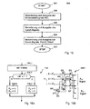
- Figures 1a and 1b show a representation of a 32 bit data word and the simplified representation of data words in a memory area of the pixel memory are stored, which is known in itself Is addressable word by word.
- a first data string and in the range of word addresses 10 to 19 is a second data string saved.
- In the second data string all binary pixel data have the value 'zero'.
- Each of the data strings consists of 10 * 32 bit data words each. To achieve high resolution double the number of data words per data string is required.
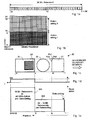
- FIG. 1 c shows a simplified print image 20 with a franking stamp image 21, postmark 22 and advertising stamp 23 and with a 2D barcode field 24.
- the latter is located in the advertising stamp drawn in, but can be arranged anywhere in the printed image 20 his.
- a printhead - not shown - can be inserted in columns Print on mail items with a print image 20 during a relative movement to the postal item, which is preferably in the franking goods transport direction (white arrow) is moved.
- Each of the stamp images is of simplicity for the sake of being reduced to an outer frame that is only for the better Representation of pixels arranged there with a Double line has been drawn.
- the printed image 20 becomes orthogonal cut print image columns arranged in the transport direction.
- a first, second and third pixel Px1, Px2 and Px3 in of the printed image column m is of a number of Print image columns 1, ..., m, ..., n, which for a column by column Pressure are meaningful.
- the latter would be an ink printing module with a single row of nozzles of image column length (EP 581 395 B1).
- Such an ink printing module is only used in special cases used and is not yet commercially available. But it will be later explained in more detail how with an arrangement of two commercially available Ink printing modules, for example from Hewlett Packard the type HP51645A, realized printing with high quality resolution becomes.
- the latter is used, for example, at a high franking material transport speed a horizontal resolution of 300 dpi and in Print column direction a maximum vertical resolution of 600 dpi reached.
- the aforementioned resolution is sufficient for a 2D barcode field 24, so that the franking goods transport speed does not continue needs to be reduced to get a higher horizontal resolution to reach.
- For franking imprints there is a slight vertical and horizontal print image resolution of 300 dpi each is sufficient in most cases.
- the tests carried out at the franking machine manufacturer one of the inks suitable for franking have shown that it It is an advantage if the print heads are only printed with every second nozzle becomes.
- Figure 1d shows a pulse / time diagram for an HR signal for a Print image according to Figure 1 c. Only when a print image column s has been reached the value of the HR signal is changed from 'zero' to 'one'. The Value can reach 'zero' when another print image column n is reached be switched back.
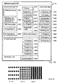
- Figure 1 e shows a representation of a data string arrangement for a Print image according to Figure 1 c.
- a position 1 there is a first data string in Column direction arranged (sawtooth patterned band).
- a first one Number of data strings - not shown in detail - each with a number Up to 320 binary pixel data can be in positions 1 ⁇ M ⁇ S-1 be arranged in columns and fill an area 220.
- Another Number of data strings - not shown in detail - each with a number up to 640 binary pixel data can be in positions S to N + K + G be arranged in columns and fill an area 230.
- the area 220 or 230 is assigned a number of data strings, each of the Loading the 320 or 640 pixel data via BUS in 20 or 40 DMA cycles 16 bits transferred to the buffer of the print data control become. When loading with only 20 DMA cycles, the BUS load is reduced.
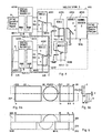
- FIG. 2 shows the block diagram of the preferred circuit arrangement for the pixel data preparation by a print data control.
- first and second print heads 1 and 2 are each via a driver unit (Pen driver board) 11 and 12 with a print data controller 4 connected, which in the case of direct memory access on the input side 16 bit parallel binary data from a BUS 5 stores and on the output side binary binary data to the driver units 11 and 12 emits.
- Via the BUS 5 are at least one microprocessor 6, a pixel memory 7, a non-volatile memory 8 and a read-only memory FLASH 9 linked in terms of address, data and control.
- An encoder 3 is included the print data controller 4 connected to the intermediate storage of the trigger binary pixel data and printing the print image columns, each printhead with a clock frequency of max.
- the print data controller 4 is supplied with at least one parameter PA via BUS 5 in order to control the resolution during printing.
- the print data controller 4 has a first and second pixel data processing unit 41 and 42 and associated controls, in particular a DMA controller 43, an address generator 44 and a printer controller 45.
- the print data controller 45 is connected directly to the microprocessor 6 via the BUS 5 and via a control line for an interrupt signal I.
- the DMA controller 43 is connected to the microprocessor 6 via a control line for DMA control signals DMA ACK , DMA REQ .
- the microprocessor 6 and the pixel memory 7 preferably have a 32-bit data bus in order to be able to access the pixel data word by word.
- An internal DMA controller of the microprocessor 6 also allows 16-bit data words to be addressed.
- the binary pixel data are made available to the two pixel data preparation units 41, 42 in data string form from the pixel memory 7.
- FIG. 3 shows a section of the circuit arrangement according to FIG. 2 with a pixel data preparation unit 42 for the second print head, with a DMA controller 43 for direct memory access (DMA), with an address generator 44 and a printer controller 45.
- DMA direct memory access
- the printer controller 45 is connected to the DMA controller 43 and the address generator 44, and the address generator 44 is connected to the pixel data preparation units 41 (not shown) and 42 in terms of control.
- the encoder 3 is connected to the printer controller 45.
- the latter is connected to the DMA controller 43 directly via control lines for first DMA control signals (DMA start, DMA busy), the DMA controller 43 receiving the DMA start signal from the printer controller 45, which results in a number of performed DMA cycles, the pixel data of the pixel data processing unit (41, 42) is made available in data strings.
- the DMA controller 43 outputs the DMA busy signal with the value 'zero' to the printer controller 45 in order to signal that the direct memory access has taken place and the DMA cycles have ended.
- the printer controller 45 is connected to the address generator 44 via at least one control line for supplying a start signal (AG start).
- the address generator 44 has - in a manner not shown here - a unit for generating read addresses and means for forming an address read signal AR as a function of the decompression factor F A , the address read signal AR corresponding to the quotient of the generated read addresses and the decompression factor F A , The latter results from an F A signal which is transmitted from the printer controller 45 via a control line 47. If a number of address read signals AR have been generated for an address group A, the address generator 44 outputs a print start signal PS via the control line 48 to the printer controller 45.
- the printer controller 45 is connected to the microprocessor 6 via a control line for an interrupt signal I and connected via the BUS 5.
- On the BUS 5 are at least the microprocessor 6, the pixel memory 7, the non-volatile memory 8 and read-only memory 9 address, data and connected in terms of control.
- the printer controller 45 has means for Generation and output of a switchover signal SO and is over a control line with the DMA controller 43 and with the pixel data processing unit 42 connected. The latter is driven to by means Switchover signal SO one of the latches 412, 422 for a transmission of pixel data to the driver unit 12. The latter can thereby the binary pixel data of an already stored Data strings are fed in groups.
- the switchover signal SO is supplied to the DMA controller 43 to control each other Select buffers 412 and 422 for loading pixel data.
- the DMA controller 43 has means for generation and output of selection signals Sel_2.1, Sel_2.2 depending on the switching state of the switching signal SO to the binary pixel data in each first or the second of the two buffers 421 or 422 caching, with a transfer of pixel data from each of the two buffers to the driver unit 12, the other buffer for buffering one Data strings can be selected one after the other by the selection signals.
- the two pixel data processing units are each on the input side at BUS 5, however, only to the low-order 16 bits of the data bus connected.
- data word or "word by word” always a 16 bit broad data word can be understood, if not expressly the Data word width is also specified.
- the pixel data for a 1 ⁇ 2 Inch printheads only take up half the space (max. 320 bits from each Data string) in the pixel memory 7, from which this pixel data of the pixel data processing unit 42 will be made available.
- a data string for consequently, both printheads require caching twice of 20 * 16 bit data words each, for example in the first Buffer is made.
- the first and second latches 421 and 422 alternately selected by the selection signals Sel-2.1 and Sel-2.2.
- the DMA controller 43 with the microprocessor 6 and connected to the buffer stores 421 and 422 for control purposes is that the DMA controller 43 has means for generating and outputting Address write signals AW, which has a DMA access to the binary pixel data stored in the pixel memory 7, the writing thereof into the buffers 421, 422 of the pixel data preparation unit 42 allow.
- the DMA controller 43 uses word-by-word addressing a 5-bit address write signal AW supplied. The latter lies each at a separate address input of the first and second Buffer 421 and 422 for pixel data for the second printhead on.
- a first selection signal Sel_2.1 for the DMA controller 43 Pixel data for the second printhead is delivered and is located on a separate Control input of the first buffer 421 for pixel data for the second printhead.
- a second is made by the DMA controller 43 Selection signal Sel_2.2 for pixel data for the second print head supplied and is located at a separate control input of the second buffer 422 for pixel data for the second printhead.
- the address generator 44 has at least means for Generation and output of address signals AR, AP and from Control signals WR, LD, PS, and wherein the address signals AR, AP and control signals WR, LD of the pixel data processing unit 41, 42 for the selection of the buffered binary pixel data and their Grouping can be supplied in a predetermined order.
- Each pixel data processing unit has two buffers, one Selector for selecting the binary pixel data and a shift register for Parallel / serial conversion of those provided in a new order binary pixel data.
- the address read signals generated by the address generator 44 AR are the caches and the selector of the Pixel data processing unit supplied.
- the address generator 44 generated primitive address signals AP and the write control signal WR become the selector and a load signal LD becomes the shift register fed.
- a start signal AG-start is sent from the printer controller 45 Address generator 44 supplied.
- the address generator 44 is now a Address read signal AR for selection of the data word with the pixel data which are intended for the second printhead. For word by word Addressing is the higher bits of the address read signal AR at a separate address input of the first and second buffers 421 and 422.
- the four least significant bits of the address read signal AR are at an address input of a second selector 423 and allow addressing within the 16-bit data word.
- the parallel data outputs of the first and second buffers 421 and 422 for pixel data for the second print head are present a first and second input of the selector 423, which from Address generator 44 controls a 14 bit parallel at its output Data signal to the parallel data input of a shift register 424 for pixel data for the second printhead.
- Shift register 424 is controlled by a shift clock signal SCL of the printer controller 45 and outputs a serial data output signal SERIAL DATA OUT 2.
- the address generator 44 has means for generating and outputting Address signals on and generates an additional address signal AS Switching of the selector 423 as long as in a register of the Printer controller 45 stores a high resolution (HR) signal becomes. In the case of a high resolution required in the printed image, a HR signal preferably stored with the value "one".
- the address generator 44 also generates a primitive address AP for control of the selector 423 and a write signal WR.
- the address generator 44 outputs a load signal LD to the shift register 424 and a print start signal PS to the printer controller 45. The latter gives the latch and
- the printer controller 45 is connected via a control line for the output of the switchover signal SO to a corresponding control input of the DMA controller 43 and to the selector 423 of the pixel data processing unit 42.
- the printer controller 45 has evaluation means for evaluating the address and control signals transmitted via BUS 5, which are evaluated with regard to the occurrence of a print command, and stores the parameters PA such as HRS, H, S required for controlling printing with different resolutions in memories.
- the printer controller 45 generates at least the signals DMA-start, AG-start, SO, F D , F A , stores the latter in registers and stands with the DMA controller 43 via control lines for DMA-start, DMA-busy, SO-, and
- F D signals in connection.
- the printer controller 45 emits a first control signal DMA-start to the DMA controller 43, the latter then generating a request signal DMA REQ and sending it to the microprocessor 6.
- the microprocessor has an internal DMA controller (not shown) which, in the case of direct memory access, applies a specific address to the pixel memory (RAM) 7, which enables binary pixel data to be transmitted word by word to the buffer stores via BUS 5.
- the address write signal AW is supplied by the DMA controller 43 to the buffer stores.
- the microprocessor 6 can read out, for example, a 16-bit data word with pixel data from the pixel memory 7 via DMA and transmit it to the print data control unit.
- the microprocessor 6 sends an acknowledgment signal DMA ACK to the DMA controller 43 in order to synchronize the generation of the address write signal AW in the DMA controller 43 with the DMA cycle of the microprocessor 6.
- the sequence of the DMA controller 43 will be explained in more detail later with reference to FIG. 12a.
- a 16-bit data word with binary pixel data arrives per DMA cycle into a buffer.
- Each of the four buffers can after every 20 DMA cycles, a total of 320 bits for further data processing provide.
- To achieve a print resolution of 600 dpi each two of the four buffers for storage during DMA cycles used.
- the DMA controller 43 therefore first and second select signals during DMA cycles Sel_2.1 or Sel_2.2 alternately to store word by word Pixel data for the second print head supplied. From the DMA controller 43 is used for alternate and word-by-word storage a first selection signal from pixel data for the second printhead Sel_2.1 and an address write signal AW delivered.
- Desired number of pixels requires a maximum of 40 data words of 16 Cache bits in two of four buffers.
- DMA control 43 become circuit means for delivering the second Control signal DMA busy and for realizing at least one cycle counter for a predetermined number of 16 bit data words.
- the binary pixel data for the first print head are supplied via BUS 5 and are at a corresponding data input of the first and second Buffer 411 and 412 for pixel data for the first printhead on.
- the first pixel data processing unit (not shown in detail) 41 for the first printhead also includes first and second Buffer 411 and 412, each of which is connected to the input side low-order 16 bits of the data bus of bus 5 connected are.
- the address write signal provided by the DMA controller 43 AW is also located at a separate address input of the first and second buffers 411 and 412 for pixel data for the first printhead.
- a first selection signal is generated by the DMA controller 43 Sel_1.1 for pixel data for the first print head delivered and is located on a separate control input of the first buffer 411 for pixel data for the first printhead. From the DMA controller 43 becomes a second selection signal Sel_1.2 for pixel data for the first Printhead supplied and is located on a separate control input of the second Buffer 412 for pixel data for the first printhead.
- the address read signal AR supplied by the address generator 44 is located likewise again at a separate address input of the first and second buffer 411 and 412 for pixel data for the first Printhead and at a first selector 413.
- the parallel data outputs the first and second buffers 411 and 412 for pixel data for the first printhead are at a first and a second input of the selector 413, which is controlled by the address generator 44 a 14 bit parallel data signal at the output of the parallel Data input of a shift register 414 for pixel data for the first Printhead supplies.
- the shift register 414 is replaced by the shift clock signal SCL controlled the printer controller 45 and gives a serial Data output signal Serial data out 1 off.
- the address generator 44 has means for generating an additional one Address signal AS to switch the selector 413 on.
- the switchover will be held up as long as in the case of an in High resolution print image required by printer controller 45 an HR signal (with the value "one") is output.
- the printer controller 45 outputs a shift clock SCL to the shift register 414 for pixel data for the first printhead and signals latch and Print1 for controlling the pen driver board 11.
- the printer control 45 is via a control line for the output of the signal SO with a corresponding control input of the DMA controller 43 and with the pixel data processing unit 41.
- the cycle counter of the DMA controller 43 is a word counter for a predetermined number of 16 bit data words, which is started by a DMA start signal.
- the DMA control is, for example, part of an application-specific circuit (ASIC), the cycle counter being connected on the one hand to the aforementioned means for generating and outputting address write signals AW and on the other hand to means for generating and outputting selection signals, the latter - in a manner not shown - have at least one output means and comparison means.
- ASIC application-specific circuit
- a first comparison means controls the output means in dependence on the SO signal in order to obtain a selection signal Sel_1.1 or Sel_1.2 intended for the first pixel data processing unit 41 until a first predetermined number of 16 bit data words has been reached, and after reaching the first a predetermined number of 16-bit data words to output a selection signal Sel_2.1 or Sel_2.2 intended for the second pixel data processing unit 42.
- the first or a second comparison means sends a signal which is present at the cycle counter in order to end the counting of DMA cycles.
- a DMA busy signal with the value 'zero' is generated from the signal and output via a register.
- the second intermediate storage 412 and 422 can be read out.
- the special Address generator 44 and selectors 413, 423 become the binary ones Pixel data from these buffers in the from the printheads read out the required order, collected in groups and then serially to the two using shift registers 414, 424 Transfer printheads. At least half a print image column is from the first print head and at least one other half of the print image column is printed by the second printhead.
- This solution enables binary pixel data in the pixel memory to be stored in one stored optimal order, which the microprocessor at Print image change relieved. Through data transfer via DMA the microprocessor also relieved.
- a data string counter is implemented in the printer controller 45 (not shown in detail), with each data string having a maximum of the above-mentioned number of 40 * 16 bit data words. After the binary pixel data taken from a data string and processed has been printed, the data string counter is incremented when the LH edge of the encoder clock occurs. When a predetermined limit value U is reached, the printing of the printed image is ended.
- the printer controller 45, the DMA controller 43, the address generator 44 and the pixel data preparation unit 41, 42 are equipped with means for switching the vertical resolution of the print image.
- the printer controller 45 is connected in terms of control to the DMA controller 43 in order to deliver at least one F D signal via a control line 46, which provides information about the vertical resolution.
- the initial value H for the F D signal is written by the microprocessor 6 into a register of the printer controller 45 via data bus 5.
- the F D signal is changed when a data string counter reaches a target value S which corresponds to a predetermined position s at a distance from the beginning of the printed image. If the F D signal with the value "one" is transmitted to the DMA controller 43, the maximum word counter setpoint is set.
- all word counter setpoints can be halved (Fig. 12) or reduced in a predetermined manner.
- the number of DMA cycles and thus the bus load is reduced and the CPU has even more time to process the program. If variable print image elements are changed, the CPU has to change less data between the frankings. This reduces the computing time required. Additional memory modules may be omitted, which reduces the manufacturing costs of the machine.
- FIG 4 is the pixel data preparation unit for the second Printhead shown in more detail.
- the first and second buffers 421 and 422 for pixel data for the second print head implemented as dual port RAM's 4210 and 4220, for example.
- Latter are selected for reading in the binary pixel data by the first or second selection signal supplied by the DMA controller Sel_2.1 or Sel_2.2 on a separate control input of each first ports 4211 and 4221 of the first and second dual port RAMs 4210 or 4220 is present.
- At the respective first ports 4211 and 4221 there is an address write signal AW when reading in pixel data.
- the previously read bits are then, for example, from the first and second dual port RAM 4210 and 4220 read out.
- the one downstream of the first dual port RAM 4210 first multiplexer 4231 is on the output side with a first data input a third multiplexer 4233 and a second dual port RAM 4220 downstream second multiplexer 4232 is on the output side connected to a second data input of the third multiplexer 4233.
- the second multiplexer 4232 has an address input 4237 for the low-order part of the address reading signal AR.
- a switchover signal is present at the control input of the third multiplexer 4233 SO so that, for example, the aforementioned single bit of the binary Pixel data is output and via a fourth multiplexer 4236 am Data input of a downstream demultiplexer 4234 is present.
- a control signal AS with the value 'one' is the first input of the fourth multiplexer 4236 switched to continuity. Otherwise by a control signal AS with the value 'zero' this passage through interrupted the fourth multiplexer 4236 and from the second input of the fourth multiplexer 4236 a voltage potential with the value 'zero' via the output of the fourth multiplexer 4236 to the data input of the downstream demultiplexer 4234.
- a control signal AS with the value 'zero' this passage through interrupted the fourth multiplexer 4236 and from the second input of the fourth multiplexer 4236 a voltage potential with the value 'zero' via the output of the fourth multiplexer 4236 to the data input of the downstream demultiplexer 4234.
- the nozzles of one of the two rows of nozzles of an ink print head corresponding to the aforementioned voltage potential and the nozzles of the other row of nozzles with the in the aforementioned manner selected variable values from the buffer accordingly driven.
- the resolution can thus be halved at least
- the demultiplexer 4234 is a resettable collective register 4235 for binary pixel data downstream, which has a 14 bit parallel data output having.
- the aforementioned single bit of binary pixel data is transferred to the collective register 4235 when a write signal WR is applied to a control input of the collective register 4235.
- the demultiplexer 4234 is supplied with a primitive address AP, which sets the storage location of the bit in the collective register 4235 and thus Ultimately, the order determines where the bit is in the data stream stands, which is transmitted serially to the Pen Driver Board 12.
- the above Collective register generated at its parallel data output successive groups of 14-bit binary data that are sent to the driver unit (pen driver board) of the 1 ⁇ 2 inch inkjet printhead.
- the associated primitive address can also be transmitted to the driver unit via the shift register (not shown).
- the shift register (not shown).
- all of the 300 binary pixel data which a 1 ⁇ 2 inch ink jet print head requires for printing are transmitted.
- the other half of the print image is printed by the first print head.
- the pixel data preparation unit for the first print head is constructed in a similar manner.
- the entire print data control can preferably be implemented using an application-specific circuit (ASIC) or programmable logic, such as, for example, Spartan-II 2.5V FPGA from XILINX (www.xilinx.com) .
- FIG. 5a shows a printed image of a franking machine with two Print heads shown in simplified form.
- the simplified printed image 20 points a franking stamp image 21, a postmark image 22 and an advertising stamp image 23 on the movement of a franking good (not shown) can be printed one after the other in the transport direction (white arrow).
- the Print image 20 is divided into two areas 201 and 202 lying in parallel, which are arranged orthogonally to the franking material transport direction, wherein the print head 1 only the area 201 and the print head 2 only the Area 202 printed when the franking material moves in the transport direction becomes.
- Each of the two areas 201 and 202 is a print field of the Print image that is orthogonal to the franking material transport direction arranged common print image columns 1 to n is cut.
- FIG. 5b shows the arrangement of the two print heads for printing the Print image on a surface of a mail piece, which is relative to the Printheads is moved in the transport direction (white arrow).
- the rows of nozzles r1, r2 of the two print heads 1 and 2 are a distance d offset to each other in the transport direction and overlap in the direction of the print image column on a route f.
- the distance d corresponds to a number of k print image columns.
- a mail piece surface runs in, on which a first number is printed on print image columns 1 to k-1 of area 202.
- the first print head 1 becomes the first print image column at the same time printed if the kth print column is already printed by the second Print head 2 is printed.
- This offset becomes binary when it is arranged Pixel data in the pixel memory taken into account.
- FIG. 6 shows a representation of pixel data for two printed fields, which are stored in the pixel memory, one print field each for Printing through a printhead is provided and in pixel memory entirely is reflected undistorted. Only the pixel data with the data value One is shown as a colored dot. The pixel data with the data value Zero are shown as a white dot. To simplify, it is assumed all the nozzles of a printhead were in a single row, which is aligned parallel to a print image column. The representation of Pixel data for the first print field begins in position 1.
- the relevant pixel data for a simplified print image are for two Printed fields before and are shown offset by a distance K, a first area 212 of a representation of pixel data for the lower half of the print image with the data value zero for pixel data in Leader 213 begins and a second area 222 of a representation of Pixel data for the upper half of the print image with the data value zero for pixel data in the trailer 223 ends.
- Both, i.e. the opening credits and Credits characterize the aforementioned offset, that in the address space of the pixel memory is to be taken into account. Because of the offset begins the display of pixel data for the second print field, which corresponds to the lower half of the printed image, only in the position K.
- a first number of binary pixel data lies in the representation of Pixel data in a position M on a line which corresponds to the position of the Print image column m in the second print image area 202 according to FIG equivalent.
- a second number of binary pixel data are in the display of pixel data in a position M + K, i.e. on another around K offset position in a line, which the print image column m in the first Reflected print image area 201 according to Figure 5a.
- the Interlaced nozzles of different nozzle rows can be a printed image with a doubled or larger number Pixels can be printed.
- the additional ones are then in the pixel memory store binary data in an appropriate order, which is a slight Change of picture elements allowed.
- FIG. 7 shows a representation of pixel data for four printed fields in pixel memory.
- the pixel data for a print image column are, for example, in four consecutive storage areas.
- Area 222 for the binary pixel data for the second row of nozzles per print head and a third area 221 and a fourth area 211 for the additional binary pixel data for the first row of nozzles provided per print head.
- the binary pixel data of the four printed fields with the data value 'one' are for the sake of simplicity connected together drawn as solid lines. At this The reflection of the printed image by the binary pixel data remains Get the shape of the picture elements of the printed image.
- FIG. 8 shows an arrangement of two print heads for printing of a printed image with a doubled resolution.
- Everyone Printhead has two rows of nozzles r11 and r12 or r21 and r22, which are at a distance g from each other.
- one Line f shown orthogonal to the transport direction, where the Nozzles in the edge area of the nozzle rows of both print heads overlap.
- the first or second row of nozzles of the two Printheads 1 and 2 are parallel to each other. Both printheads 1 and 2 are spaced apart by a distance d in the transport direction.
- each of the print heads 1, 2 begins the representation of - shown in FIG Pixel data for that through the first nozzle row r21 of the second Third print field to be printed only in position G.
- FIG. 9a shows a representation of pixel data for four printed fields in the pixel memory for a preferred arrangement of the pixel data.
- the pixel memory gives an identical image of the pixels with even ones Numbers of a first print image column and the pixels with odd Numbers of a second printed image column that are about 1 ⁇ 2 inch wide an inkjet print head with two rows of nozzles.
- a pattern with such data strings arranged in columns - as in 9a is shown - thus gives an identical image of the through an inkjet printhead with a part of the printout about 1 ⁇ 2 inch wide Frankierstempeltiksentes.
- the binary pixel data from the same Print head to be printed are in the same area 201 or 202 and are in adjacent data strings arranged in columns shown. The same applies to both areas Order of the data strings.
- the binary pixel data for print fields that can be assigned to different rows of nozzles of the same printhead, are shown in the same area 201 and 202 in staggered positions, i.e. the binary pixel data the print fields of one half of the print image can be stored in the pixel memory be nested one after the other.
- the representation of the binary Pixel data of the two print fields for the two rows of nozzles the same printhead is in an area 202 which is the top half of the Print image reflects, dotted. Every point should be a reflect binary pixel date with the data value 'one'.
- the data string shown in the first position are the binary ones Pixel data for the nozzles of the nozzle row with an even number or the binary pixel data for the nozzles with an even number and for example have the data value 'one'.
- the binary pixel data for the Nozzles of the nozzle row with an odd number or for all odd number of nozzles that are in the data string at the first position is shown, for example have the data value 'zero'.
- the binary pixel data for the nozzles of the row of nozzles with an even number or for all nozzles with an even number that is in the data string that is on the Position G is shown, for example, have the data value 'zero'.
- the binary pixel data d210 of the frame of the franking stamp image are for two print fields each in offset positions (for example, M and M + G) but are saved when you print one Print image column (for example m) as two ideally one above the other Rows of pixels printed out at different times, so that practically a single line in after printing Direction of image column result. Only to distinguish the reflection the lower half of the printed image was in another Area 201 of Figure 9a uses a solid thick line to also the binary pixel data of the two print fields for each two rows of nozzles of the other printhead as a simple pattern display.
- a print image column m shown, in which both of the above rows Pixels are falling.
- a first pixel then becomes a first pixel from row r1 Px1 and a first pixel Px2 is printed by a second row of nozzles r2, which are at a distance h orthogonal to the transport direction.
- Such a print image column exists with data words in the pixel memory binary pixel data for nozzles with odd or even numbers. ever The data word is stored in 32 bits. These data words are each Assigned addresses.
- FIG. 10a shows a representation of the binary pixel data of a picture element for an arrangement of two printheads with only one Row of nozzles, according to Fig. 5b.
- the binary pixel data is in a portion of the pixel memory stored.
- E of a picture element are those binary pixel data as black Pixels are shown which have the value 'one'. The value becomes 'zero' not shown in color.
- Ten data words W1 to W10 of 32 bits each Binary data form a data string with binary pixel data Printing a print image column with a row of nozzles is required.
- a The first data string of 320 binary pixel data is on the right in FIG. 10a represented by white dots in position 1 on a row lie.
- the display ends with a data string on the Position M + L and there was only one with the first three data words W1, W2 and W3 of a data string addressable area contiguous with which only about a third of those for 300 nozzles required binary pixel data is addressable. But that's not supposed to Limit for a representation of data strings. A practical one Limitation results only from the maximum number of data words. Which can be stored in a pixel memory.
- the in the Representation used numbering corresponds to the binary pixel data numbering the nozzles in a row of nozzles and starting for everyone Data string with the number one in the first group.
- the numbering the binary pixel data of the tenth group ends with the Number 320.
- each data string is repeated until position M is reached.
- the picture element E can already use a first data word W1 can be addressed. This is repeated up to position M + L and thus arises because each binary value 'one' is represented as a black dot is the illustration E of the image element as a black box.
- the aforementioned black box becomes 12 pixels long and 6 pixel wide pixel field with a resolution of 600 * 300 dpi through one of the two printheads with a single row of nozzles printed.
- a data matrix code has 48 x 48 picture elements.
- FIG. 10b shows a representation of the binary pixel data of a picture element, which is stored advantageously divided in the pixel memory.
- the binary pixel data of a picture element for the nozzles with a straight line Number D # and for the nozzles with an odd number D # are in different data strings always in the same data word.
- both figures are in the first data word of different data strings.
- the binary pixel data with the data value 'One' for the nozzles in the nozzle row with an even or odd one Number or in other words, for the odd or even numbers of the nozzles are located in data strings at the position M ⁇ E1 ⁇ position M + L or at the position M + G ⁇ E2 ⁇ position M + G + L.
- the binary Pixel data with the data value 'one' and with the same data number from immediately adjacent data strings were only for illustration purposes not represented as a dot, but as a thick black line.
- the stored binary pixel data of a picture element are included both representations of Figures 10a and 10b each within a 32nd Bit data word W1.
- no further 32 bit data words are required be called, especially if variable picture elements be changed from print to print. So that computing time of Microprocessor saved.
- a pixel memory is therefore preferably used Organized order, which already explained in connection with Fig.9a and which makes it possible to reduce the number of data words, which must be called by the microprocessor to create a picture element to change.
- FIG. 10c shows a representation of the binary pixel data of a picture element stored in a known manner in the pixel memory, the pixel data being arranged in the pixel memory in such a way that they can be read out one after the other during printing.
- an image E2 of binary pixel data with even data numbers D # and an image E1 of binary pixel data with odd data numbers D # the binary pixel data with the data value 'one' and with the same data number being shown as a thick black line are.
- the even data numbers D # and odd data numbers D # of the stored binary pixel data in the representation according to FIG.
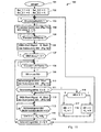
- FIG. 11 shows a flow chart for the sequence control of the printer control.
- step 102 is reached and all selection signals Sel_1.1, Sel_1.2, Sel_2.1, Sel_2.2 are set to the value 'zero' in the routine 100 of the sequential control system.
- a data word transmitted via BUS 5 is now evaluated with regard to the occurrence of a command to start printing. If the latter has not yet been granted, the system branches to a waiting loop.
- the data string count value V is set to the initial value 'zero' in a step 104.
- a binary changeover signal SO is set to the value 'one'.
- an HR variable that can be switched between two values is set to an initial value HRS, which is present in a register of the pressure control.
- the initial HR value and the compression or decompression factors F D or F A derived therefrom are stored in registers of the printer controller, which is explained in more detail with reference to FIGS. 16a, b.
- the corresponding registers with the F D or F A variables are queried in subroutines 106 and 112 and 110.
- a signal DMA start is output in a step 106 and a subroutine 300 is started, which certain selection signals Sel_1.1, Sel_1.2, Sel_2.1 or Sel_2.2 sets to the value 'one' in order to binary pixel data in the buffer of the pixel data processing units 41 and 42 to take over what is shown in FIG 12 later is explained in more detail.
- a third query step 107 the DMA busy signal is now evaluated with regard to whether it has been set to the value 'zero'. If the latter is not yet the case, the system branches into a waiting loop. However, if the DMA busy signal has been set to the value 'zero', a fourth query step 108 is reached in which the encoder signal is evaluated with regard to the occurrence of an LH edge. If the latter has not yet occurred, the system branches to a waiting loop. On the other hand, the switchover signal SO is logically negated in a step 109 and then output.
- the address generator is then activated in step 110 and a subroutine 400 is started which generates read addresses AR and control signals, such as the additional address signal AS, the primitive address AP, the write signal WR and a load signal LD, which are intended for the pixel data preparation units 41 and 42.
- the data string count value V is queried whether the latter has reached the target value S. This corresponds to a position s in the print image to which the target value S is assigned (FIG. 1e).
- the process branches to step 112 if the data string count V has not yet reached the target value S.
- a DMA start signal is output and the DMA controller is activated to restart the aforementioned subroutine 300.
- step 115 it is evaluated whether the column count V has reached a limit value U. If this is not yet the case, the system branches to the fourth query step 108. Otherwise, a branch is made to the first query step 103 and the routine starts again when a print start command is determined in the first query step 103.
- the address generator then works with a decompression factor F A which differs in value from the value of the compression factor F D for the following data string to be loaded into the buffer.
- the process then branches from steps 117 or 118 to step 112 in order to output a DMA start signal.
- the pixel data of an odd nozzle number are in a different print column than the pixel data in the print image an even nozzle number, even though the pixel data becomes a data string belong and printed together in the same time period become.
- the ones for the second print head are determined in the print image Pixel data with an odd and even nozzle number, in two other print columns printed. In the transition area, a gradual transition in the printed image between high and low resolution and vice versa.
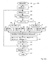
- FIG. 12a shows a flow chart for DMA control.
- a subroutine 300 is called when a DMA start signal is output from the printer controller 45 to the DMA controller 43 (step 301).
- a word count W is set to the value 'zero'.
- a DMA busy signal is set to the value 'one' and transmitted to the printer controller 45.
- a DMA request signal DMA REQ with a value 'zero' is transmitted to the microprocessor 6. The latter transmits an acknowledgment signal DMA ACK to the DMA controller 43.
- a first query step 304 of the subroutine 300 if the acknowledgment signal DMA ACK is not received, the system branches to a waiting loop with a value of 'zero'. From the first query step 304 of the subroutine 300, when the acknowledgment signal DMA ACK is received, the value jumps to a second query step 305, with the state of the switchover signal SO being determined. If the switchover signal SO has the state equal to one, then a branch is made to a third query step 306. Otherwise, the switchover signal SO has the state 'zero' and a branch is made to a fourth query step 309. In the third query step 306 it is checked whether the word counter has a value W less than the quotient of twenty divided by F D.
- step 307 the first selection signal for the first print head Sel_1.1. switched to the value 'one' and the address write signal AW receives the current value W of the word counter.
- step 312 the pixel data are transferred to the buffer stores of the pixel data change units 41, 42. Then in step 313 all selection signals are switched to the value 'zero' and a DMA request signal DMA REQ with a value 'one' is transmitted to the microprocessor 6.
- step 314 the word count W is incremented by the value 'one'.
- step 315 it is checked whether the word counter has a value W less than the quotient of forty divided by F D. In this case, in which the word counter has such a value W ⁇ 40 / F D , the method branches back to step 303.
- a branch is made to a step 316 in order to output a signal DMA-busy with the value 'zero' before the end (step 317) of the subroutine 300 has been reached. Otherwise, if it is determined in the third query step 306 that the word count W is not less than twenty divided by F D , then a branch is made to a step 308 in which the first selection signal for the second print head Sel_2.1. is switched to the value 'one' and the address write signal AW receives the current value W of the word counter reduced by the value of the quotient 'twenty divided by F D '. In the subsequent step 312, the pixel data are again transferred to the buffer.
- step 309 it is also checked whether the word counter has the predetermined value W ⁇ 20 / F D , wherein it was previously determined in query step 305 that the binary switchover signal SO does not have the value equal to one. If the word counter has the predetermined value W ⁇ 20 / F D , then in step 310 the second selection signal for the first print head Sel_1.2. switched to the value 'one' and the address write signal AW receives the current value W of the word counter. In the subsequent step 312, the pixel data are again transferred to the buffer.
- the fourth query step 309 branches to a step 311 in which the second selection signal for the second print head Sel_2.2 is switched to the value 'one' and that Address write signal AW receives the current value W of the word counter reduced by the value of the quotient 'twenty divided by F D '.
- the pixel data are again transferred to the buffer.
- FIG. 12b shows a block diagram of a DMA controller.
- the DMA controller 43 has at least one sequencer 4301, a word counter 4302, a setpoint register 4303, an input / output logic 4304, a memory 4305, a comparator 4306 and a shift register 4307, which are interconnected to perform DMA cycles.
- a further processing unit can be integrated into the sequence control 4301, with which the aforementioned blocks 4302 to 4307 are connected in terms of circuitry.
- the aforementioned switching of the number of data words can be carried out with a shift register, since one digit shift of binary numbers corresponds to a division by the number two and a further shift to a division by the divisor four derived from the number two.
- the input / output logic 4304 has at least one input 43041 for the transmitted compression factor F D , one input 43042 for the received DMA start signal and registers 43043 to 43046 for the select signals to be sent, a register 43047 for the DMA busy signal to be sent, a register 43048 for the request signal DMA REQ to be sent , an input 43049 for the received Acknowledgment signal DMA ACK , an input 43050 for the switchover signal (SO) and register 43051 for the address write signal AW.
- the input / output logic 4304 has at least one input 43041 for the transmitted compression factor F D , one input 43042 for the received DMA start signal and registers 43043 to 43046 for the select signals to be sent, a register 43047 for the DMA busy signal to be sent, a register 43048 for the request signal DMA REQ to be sent , an input 43049 for the received Acknowledgment signal DMA ACK , an input 43050 for
- the type of logic of the specific embodiment of the DMA control can be selected as desired and there are a large number of suitable design variants.
- Hardware implementation of the DMA controller is possible in a manner known per se, for example using an ASIC or advantageously using an FPGA (Field Programmable Gate Array).
- Figure 13a shows a flow chart for address generation.
- the addresses of stored binary pixel data begins with both printheads with the start address zero, which is the following for the address read signal AR is generated.
- a register for the AG busy signal is set to the value 'One' set.
- step 403 the question is asked whether the numerical value P of the counter of the primitive address is equal to the value one. If this is the case, the second query step 404 is reached. Here it is determined whether the counter A has reached the value 8 or 9 or 15 or 16. If this is the case, step 406 is carried out and the numerical value 255 is subtracted from the numerical value C of the counter of the address read signal AR.
- the subsequent step 418 is used to select read addresses and has a number of sub-steps.
- the third query step 418.1 it is determined whether the decompression factor F A is equal to the value 'one'. With high resolution, this is always the case and sub-step 418.2 is reached, in which the register for B is set to the value 'zero' and the additional address signal AS is changed to the value 'one', as a result of which the fourth multiplexer in the selector for binary pixel data is switched to continuity.
- After the first address read signal AR further address read signals AR with other predetermined values are generated.
- a selection can be made at the beginning by a corresponding choice of the value Q as to whether the read addresses generated to be assigned to even-numbered primitive addresses P should be ignored or selected in order to generate an address read signal AR. If the value Q is set to the value 'zero' at the beginning, then each of the read addresses which can be assigned to even-numbered primitive addresses P is selected. If the value Q is initially set to the value 'one', then each of the read addresses which can be assigned to odd-numbered primitive addresses P is selected.
- the decompression factor F A 2 or 4, which is why a further query step 418.5 branches off and checks whether the decompression factor F A is equal to the value 'two'. If this is the case, the process branches to sub-step 418.2, in which the register for B is set to the value 'zero' and the additional address signal AS is changed to the value 'one', which causes the fourth multiplexer in the selector for binary pixel data to pass through is switched.
- the method branches to query step 418.6, in which it is determined whether a count value A for the address group is an even number. If the count value A is odd, the process branches back to sub-step 418.2. If there is an even number A, the program branches to sub-step 418.4. Otherwise, a branch is made to sub-step 418.4 if it was determined in query step 418.3 that the register for B is not equal to the value 'one'. In query step 418.4, the register for B is set to the value 'one' and the additional address signal AS is changed to the value 'zero'.
- the respective fourth multiplexer in the selector is switched to the switching state (not shown in FIG. 4) and outputs a binary pixel data with the value 'zero' at its output.
- step 425 the numerical value for the counter of the primitive address AP output.
- step 426 a write signal WR for the Entry of the binary pixel date in a collective register.
- step 427 changes the numerical value for the counter of the primitive address AP increments the value 'one'.
- step 428 reached and it is found that the numerical value P of the counter of the Primitive address AP has not yet reached the limit value 15. The system then branches back to the first query step 403.
- the numerical value P of the counter of the primitive address is not equal to the value 'one' and at sixth query step 407 branches. If the numerical value P is odd then a branch is made to the seventh query step 408, in which it is checked whether the counter of the address group has the value 8 or 15. If this is the case, then a branch is made to step 409 and to Numerical value C of the counter of the address read signal AR becomes the Numerical value 3 added. Otherwise, the seventh query step 408 branches to a step 410 and to the numerical value C of the counter of the address read signal AR, the numerical value 47 is added.
- the sixth Query step 407 branches to the eighth query step 415, in which it is checked whether the counter of the address group has the value 8 or 15. If this is the case, then a branch is made to step 416 and to Numerical value C of the counter of the address read signal AR becomes the Numerical value 41 added. Otherwise, the eighth query step 415 branches to a step 417 and to the numerical value C of the counter The numerical value 3 is subtracted from the address read signal AR.
- the query step 418.1 is reached again and it is found that, for example, low resolution, ie the decompression factor F A not equal to the value "one", was selected at the beginning.
- the query step 418.3 is reached again and it is found that the register for the variable B is set to the value 'zero', for example, that is to say is not equal to the value 'one'.
- the process then branches to step 418.4 and the additional address signal AS is changed to the value 'zero', as a result of which the fourth multiplexer in the selector is switched.
- Step 429 branches and a load signal LD to load the shift register issued.
- step 430 output a PS signal and a subroutine 500 to output the Pixel data started.
- the printer controller 45 operated after receiving the PS signal a shift clock signal SCL to the shift register to output the pixel data serially from the latter.
- FIG. 14 shows a table for address generation by the aforementioned routine 400.
- the address generator 44 preferably generates the address values as a binary number and applies them to the pixel data preparation units 41, 42.
- a binary number can be represented, for example, as a hexadecimal or decimal number, which means that the representation requires less space. Only for this reason and for better understanding, decimal numbers are entered in the table.
- the address values greater than 500 Therefore, it does not have to be possible to generate the binary number completely.
- To the Providing binary pixel data makes all address values larger created as 299, but also not required for printing.
- Routine 400 continues to run until all print image columns have been printed.
- Rows of nozzles of a printhead become active alternately. But with Low resolution printing requires only one row of nozzles to be active.
- the selected row of nozzles of the print head can of course be changed on a print image basis. In such a case, the unselected row of nozzles in the print head pauses until the next print image. This prevents one of the two rows of nozzles from being used excessively and prevents premature failure of the print head.
- the other cache read out to the processed groups of binary pixel data Transfer driver units.
- the mutual repetition of the Routine 400 and other subsequent steps are performed by the Printer control 45 executed controlled, which in turn by controlled by a signal e of an encoder 3, also the print signals Print 1 or Print 2 generated.
- FIG. 15 shows a flowchart of the output routine 500.
- the latter is called as a subroutine in the course of subroutine 400, around the shift registers in the print data controller 41, 42 and around the Control driver units (Pen Driver Boards) 11, 12.
- a step 502 is reached and a skid clock SCL generated to the via the serial data output from the shift register in the latter loaded pixel data for the respective driver unit 11, 12 continue to push.
- step 503 a latch signal generated and to the driver units (pen driver boards) 11, 12 output.
- step 504 the print signals Print1, Print2 generated and output to the driver units (pen driver boards) 11, 12 and in step 505, subroutine 500 is stopped.
- each data string there is a first or second number of data words, the binary pixel data for first and second ink jet printheads, respectively 1, 2 included.
- the binary pixel data for first and second ink jet printheads respectively 1, 2 included.
- each inkjet printhead 1, 2 each printed out one half of each print image column, with the first and second row of nozzles of each ink jet printhead simultaneously the pixels with odd numbers on at least half of one first print image column and the pixels with even numbers at least printed on one half of a second print image column.
- Each data string becomes the first in the transport direction lying row of nozzles staggered with the binary pixel data for the pixels with odd numbers of the first print image column, while the second in the transport direction Row of nozzles already with the binary pixel data for the pixels with even Numbers of the subsequent further print image column is supplied.
- each Half of the printed image column is separated by the first and second row of nozzles each ink jet printhead, with each print column column half completed after printing with the second row of nozzles by printing with the first row of nozzles.
- the first print image column is thus separated from the second print image column in Transport direction printed out spaced, both print image columns wider for some types of printheads and very close for other types lie together.
- FIG. 16a shows a detail of the flow chart according to FIG. 11 with the sequence control of the printer control.
- step 104 the HR register in the printer controller is loaded with a start value HRS in sub-step 104.1.
- FIG. 16b shows a logic 4501 in one embodiment with NAND gates, which executes the sub-steps 104.2, 104.3 and 104.4. The latter are part of step 104 shown in FIG. 16a. NAND gates and other registers, not shown, are required to implement the flowchart.
- a value specified by the aforementioned circuit means, for example H 4, is called a binary number 1 * 2 2 ; 0 * 2 1 ; 0 * 2 0 and on the input side to gates G2, G4, G6 of logic 4501, which outputs the 3-bit F D signal or F A signal on the output side via gates G3, G5, G7 depending on the HR signal , which is also present on the input side of gate G1 on logic 4501.
- a minimal variant with a 1-bit wide F D signal or F A signal has not been shown separately, but can easily be derived from it for switching from the maximum to half the resolution or vice versa. This eliminates the higher significant digits of the dual number and thus four of the seven gates, ie all except G1, G2 and G3.
- An alternative embodiment based on NOR gates can also be used. The embodiment and the specific interconnection depend on the type of hardware ASIC or FPGA used and are implemented by means of a development tool which runs as an application program on a computer and implements an interconnection of assemblies of the ASIC or FPGA.
- an FPGA up to one hundred thousand gate equivalents (for example NAND) are available in order to implement such circuit variants with a very large number of gates (for example NAND) essentially using a commercially available module.
- FIG. 13b shows a block diagram of an embodiment of the address generator. It is provided that the address generator 44 has an input / output logic 444 and a selection logic 442, which is connected between the unit 441 for generating read addresses and the means 443 for forming the address read signal AR, that the selection logic 442 for selecting read addresses is dependent is operated by the decompression factor F A.
- the selection logic 442 generates the additional address signal AS, which is applied to the selector 413, 423.
- a voltage potential with the value 'zero' is applied to supplement the pixel data missing due to the compression. Switching to the voltage potential with the value 'zero' takes place when the additional address signal AS has the value 'zero' (FIG. 4).
- the unit 441 for generating read addresses there is a first counter 4410 for the primitive address and an assigned first comparator 4411 for comparing a count value P of the primitive address with a first setpoint value, which is supplied by a first setpoint register 4412, and a second counter 4413 for an address group and an assigned second comparator 4414 for comparing a count value A of the address group with a second setpoint value, which is supplied by a second setpoint register 4415, and a sequence control 4401.
- the latter works together with a calculation unit 4402 for parameter C, a WR signal generator 4403, an LD signal generator 4404, a PS signal generator 4405, with counters 4410 and 4413, with comparators 4411 and 4414, with registers 4412 and 4415 as well as an AG busy signal generator 4416 and possibly with another switchover logic 4417 (shown in broken lines), the comparison in the first comparator after formation of the address read signal AR and after incrementation of a count value P for the primitive address by the value 'one' is carried out, in which a number of read addresses are successively generated, a setpoint value is exceeded or the counter for the primitive address is overflowed, a load signal LD is output and a subroutine is started for output, the counter for an address group by the value 'one' is incremented, with falling below the second setpoint when comparing in the second comparator an R ckwishing the count value P of the primitive address to the value 'One' and a generating triggers a subsequent read address that is associated with another address
- the input / output logic 444 of the address generator 44 has an input 4441 for the transmitted decompression factor F A , an input 4442 for receiving an initial value Q for a variable B, a register 4443 for the additional address signal AS, and an input 4444 for receipt of the address generator start signal and a register 4445 for the address generator busy signal to be sent, that the selection logic 442 has a register 4423 for the variable B and a first comparison logic 4421 for generating the additional address signal AS with the value 'zero', which is generated if both the variable B and the decompression factor F A transmitted by the printer controller 45 in the F A signal are set to a value not equal to the value 'one' or if the decompression factor F A is set to a value not equal to the value 'one' and the variable B is equal to the value 'one' and the decompression factor F A is not equal to a value ch is set to 'Two' and the count A of the address group is an even number.
- the selection logic 442 also has a second comparison logic 4422 for generating the additional address signal AS with the value 'one', which is generated when the decompression factor F A transmitted by the printer controller (45) in the F A signal has the value 'one' is set.
- the second comparison logic 4422 has further comparison means 4424 for generating the additional address signal AS with the value 'one', which is generated when the decompression factor F A is set to a value not equal to the value 'one' and the variable B is equal to the value 'one''and the decompression factor F A is set to a value equal to the value' two 'or the decompression factor F A is set to a value not equal to the value' two 'and the count value A of the address group is not an even number.
- register 4423 for variable B the value is set to 'one' set if the selection logic generates the additional Address signal AS with the value 'zero' takes place. With every generation of the additional address signal AS with the value 'one' is from the Selection logic of the value in the register for variable B to the value 'zero' reset.
- Another comparator 4425 in the selection logic 442 is provided so that the address read signal AR only from read addresses with one positive value is generated. This corresponds to query step 418.7 according to Figure 13a.
- the means of the AR generator 443 include a shift register 4431, in which a binary number stored in accordance with the generated read address is shifted by at least one digit if a decompression factor F A is present at the input 4441 of the address generator 44, which has a value 'One' differs.
- the unit 441 for generating a read address has a number of counters which are connected in order to couple the formation of the address read signal AR with a primitive address signal AP, so that each count value P for the primitive address is repeated and each count value P is one Number of read addresses can be assigned, with the selection logic selecting at least one group of read addresses depending on the variable B and the decompression factor F A.
- the sequence controller 4401 is provided with a calculation unit 4402 for the Parameter C with a signal generator 4403 for generating a write signal WR, with a signal generator 4404 for generating a loading signal LD, with another signal generator 4405 to generate a Print start signal PS for causing printing of the pixel data from a data string and connected to a busy signal generator 4416.
- the input / output logic 444 of the address generator 44 has a register 4446 for the delivery of the primitive address AP, a register 4447 for the Write signal WR, a register 4448 for the load signal LD, a register 4449 for the output of the address read signal AR and a register 4440 for the output of the print start signal PS.
- the fourth multiplexer 4136 or 4236 with its output - according to FIG. 4 - at the data input of a downstream demultiplexer 4134 or 4234 is omitted, if the function of the first and second multplexer 4131 and 4132 or 4231 and 4232. If another Data input at which an additional voltage potential with the value 'Zero' is present by means of the additional address signal AS, which as Part of the address read signal AR is generated on the output of the first and second multiplexers 4131 and 4132 or 4231 and 4232 is switched through, the - shown in Figure 3 - separate Control line to the pixel data processing unit is eliminated.
- FIG. 17 shows a block diagram for a printer controller 45.
- An input / output unit 454 and at least the following blocks are connected to a sequence controller and processing unit 451, a parameter determiner 4501, a parameter changer 4502, a V counter 4503, a comparator 4506, a V soll -Register 4504, a memory 4505, a shift pulse generator 4507, a latch pulse generator 4508, a first print pulse generator 4509 and a second print pulse generator 4510, a logic 4511 and possibly a switching logic 4517.
- the input / output unit 454 has at least the following blocks, a BUS input / output unit 4541, an input 4542 for the encoder signal e, an input 4543 for the DMA busy signal, a register 4544 for the DMA start signal, one Input 4545 for the AG busy signal, a register 4546 for AG start signal, a register 4547 for the switchover signal SO, an F A register 4548, an F D register 4549, an input 4550 for the PS signal , an output 4551 for the I signal, an output 4553 for the shift clock signal, an output 4554 for the latch pulse signal, a Print1 pulse output 4555 and a Print2 pulse output 455x.
- a Q register 4552 in the I / O unit 454 transfers an initial value Q to the address generator 44.
- the printer controller 45 can also in the already explained or in an alternative embodiment, each Printer controller 45 - regardless of the embodiment - one Has data string counter 4503 and is connected to the encoder 3. After each printed data string the value V becomes the data string counter incremented when the encoder clock occurs, the value of the high-definition signal HR is changed when a predetermined one first setpoint S of the data string counter is reached, and the Printing of the printed image is terminated when a predetermined second Target value U of the data string counter has been reached.
- a parameter changer 4502 with interconnected ones is advantageous NAND gates provided that performs the same function.
- the logic 4511 of the printer controller 45 is provided in order to adjust the decompression factor F A to the current compression factor F D when the DMA controller 43 and the address generator 44 send out a busy signal with the value 'zero'.
- the corresponding parameters for at least one further setpoint V soll2 of the data string counter and an associated value for the resolution H can be loaded into the memory 4505 of the printer controller 45.
- the respective next desired value V soll2 is transferred to the register 4504 after the query step 111 of the routine 100 has been carried out (FIG. 11).
- the corresponding parameters between the Print or programmed during printing from which Data string number with which resolution is printed.
- the corresponding parameters are preset or permanently programmed, from which data string number with which resolution is printed.
- a further - dashed lines - switching logic 4517 is arranged to the initial value Q for the address generator in synchronism with the switchover signal SO 44 to change, so the rows of nozzles of a printhead be operated alternately.
- the initial value Q is over a separate control line to the Q input of the address generator 44 transmitted.
- control line for the changeover signal SO continued to the address generator 44, which then by means of a other - dashed lines - switching logic 4417 itself synchronously generates an initial value Q for the switchover signal SO.
- an SO input is then implemented. With an initial value of Q with the value 'one' the first generated read address is selected as well as the following and each further one of an even-numbered primitive address assignable read address ignored At an initial value Q with the If the value is 'zero', the first generated read address is ignored and the following and each further assignable to an even primitive address Reading address selected.
- the print head has only one is equipped with a single row of nozzles for printing a print image column
- the order of the binary pixel data in the data string matches the Order of the pixels in the print image column match.
- the order of the binary pixel data then corresponds to the print head type even changed image-by-image columns during printing.
- the arrangement of binary pixel data in the pixel memory RAM 7 can advantageously be organized in such a way that a change of picture elements is easy or inexpensive.
- the order of the binary pixel data within a data string can advantageously be changed according to the print head type during printing.
- the number of binary pixel data within each data string can advantageously be reduced within a printing section, the latter being generated in compressed form and being stored in the pixel memory in the form of 16-bit data words.
Landscapes
- Engineering & Computer Science (AREA)
- Physics & Mathematics (AREA)
- General Physics & Mathematics (AREA)
- General Engineering & Computer Science (AREA)
- Theoretical Computer Science (AREA)
- Computer Security & Cryptography (AREA)
- Record Information Processing For Printing (AREA)
- Dot-Matrix Printers And Others (AREA)
Abstract
Description
- Figur 1 a,
- Darstellung eines 32 Bit-Datenwortes,
- Figur 1 b,
- Vereinfachte Darstellung von gespeicherten Datenwörten,
- Figur 1 c,
- Vereinfachtes Druckbild eines Frankierabdruckes,
- Figur 1d,
- Impuls/Zeit-Diagramm für ein HR-Signal für ein Druckbild nach Figur 1 c,
- Figur 1 e,
- Darstellung einer Datenstringanordnung für ein Druckbild nach Figur 1 c,
- Figur 2,
- Blockschaltbild für die Pixeldatenaufbereitung durch eine Druckdatensteuerung,
- Figur 3,
- Ausschnitt aus der Schaltungsanordnung nach Fig.2 mit einer Pixeldatenaufbereitungseinheit für den zweiten Druckkopf,
- Figur 4,
- Pixeldatenaufbereitungseinheit für den zweiten Druckkopf,
- Figur 5a,
- Druckbild für eine Frankiermaschine mit zwei Druckköpfen,
- Figur 5b,
- Anordnung der zwei Druckköpfe zum Drucken des Druckbildes,
- Figur 6,
- Darstellung von Pixeldaten für zwei Druckhalbbilder im Pixelspeicher,
- Figur 7,
- Darstellung von Pixeldaten für vier Druckhalbbilder im Pixelspeicher,
- Figur 8,
- Anordnung der zwei Druckköpfe zum Drucken des Druckbildes mit einer verdoppelten Auflösung,
- Figur 9a,
- Darstellung von Pixeldaten für vier Druckhalbbilder im Pixelspeicher, in einer bevorzugten Anordnung,
- Figur 9b,
- Darstellung zum spaltenweisen Druck von Pixeln,
- Figur 10a,
- Darstellung der in einem Pixelspeicher gespeicherten binären Pixeldaten von einem Bildelement,
- Figur 10b,
- Darstellung der binären Pixeldaten eines Bildelementes, das vorteilhaft aufgeteilt im Pixelspeicher gespeichert ist,
- Figur 10c,
- Darstellung der in bekannter Weise gespeicherten binären Pixeldaten eines Bildelementes im Pixelspeicher,
- Figur 11,
- Flußplan zur Ablaufsteuerung der Druckersteuerung,
- Figur 12a, b,
- Flußplan und Blockschaltung zur DMA-Steuerung,
- Figur 13a, b,
- Flußplan und Blockschaltung zur Adressengenerierung,
- Figur 14,
- Tabelle zur Adressengenerierung,
- Figur 15,
- Flußplan der Ausgaberoutine,
- Figur 16a, b,
- Detail zur Ablaufsteuerung nach Fig.11,
- Figur 17,
- Blockbild der Druckersteuerung,
- Figur 18,
- Darstellung verschiedener Druckauflösungen.
Claims (29)
- Anordnung zum Drucken eines Druckbildes mit Bereichen unterschiedlicher Druckbildauflösung auf ein bewegtes Postgut in einem Postbearbeitungsgerät mit einem Druckkopf (1, 2) der über eine Treibereinheit (11, 12) von einer Druckdatensteuerung (4) ansteuerbar ist, die mit einem Encoder (3) und über einen BUS (5) mit mindestens einem Mikroprozessor (6), einem Pixelspeicher (7), einem nichtflüchtigen Speicher (8) und einem Festwertspeicher (9) adress-, daten- und steuermäßig verbunden ist, gekennzeichnet dadurch, dass der Mikroprozessor (6) so programmiert ist, unter Verwendung von Daten aus dem Festwertspeicher (9) eine Anzahl an Datenstrings mit einer umschaltbaren Anzahl an Datenworten zu generieren und im Pixelspeicher (7) zu speichern, wobei eine maximale Anzahl an Datenworten je Datenstring unterschritten wird, wenn die Pixeldaten komprimiert gespeichert werden, dass die Druckdatensteuerung (4) zur Pixeldatenaufbereitung während des Druckens mit dem Druckkopf (1, 2) ausgebildet und mit Mitteln ausgestattet ist, die komprimierten Pixeldaten je Datenstring zu dekomprimieren und dabei die aufgrund der Komprimierung fehlenden Pixeldaten so zu ergänzen, dass die Verringerung der Anzahl an Datenworten je Datenstring der Reduzierung der Auflösung bei Drucken entspricht, dass der Mikroprozessor (6) programmiert ist, mindestens einen Parameter (PA) zur Steuerung der Auflösung via BUS (5) der Druckdatensteuerung (4) zuzuführen und dass die Druckdatensteuerung (4) dazu ausgebildet ist, die beim Drucken erzielbare Auflösung umzuschalten.
- Anordnung, nach Anspruch 1, gekennzeichnet dadurch, dass der Mikroprozessor (6) programmiert ist, für Hochauflösung einen Anfangswert (HRS) via BUS (5) zur Druckersteuerung (45) zu übermitteln, dass die Druckdatensteuerung (4) aus einer Pixeldatenaufbereitungseinheit (41, 42), einer DMA-Steuerung (43), einem Adressengenerator (44) und einer Druckersteuerung (45) besteht, wobei die Druckersteuerung (45) steuerungsmäßig mit der DMA-Steuerung (43), dem Adressengenerator (44) und der Pixeldatenaufbereitungseinheit (41, 42) verbunden ist.
- Anordnung, nach den Ansprüchen 1 bis 2, gekennzeichnet dadurch, dass die Druckersteuerung (45) mit Mitteln zur Generierung von Signalen entsprechend den Faktoren (FA, FD) ausgestattet ist, wobei die Faktoren (FA, FD) gleich dem Wert 'Eins' des Anfangswertes (HRS) oder verschieden vom Wert 'Null' des Anfangswertes (HRS) sind, wobei die Faktoren (FA, FD) mindestens gleich dem Wert 'Zwei' gesetzt sind, wobei die DMA-Steuerung (43) durch ein über eine Steuerleitung (46) übermitteltes FD-Signal umschaltbar ist, so dass beim Laden von binären Pixeldaten in einen Zwischenspeicher (411, 421 bzw. 412, 422) der Pixeldatenaufbereitungseinheit (41, 42) die Anzahl an DMA-Zyklen mindestens halbiert ist und wobei der Adressengenerator (44) durch ein über eine Steuerleitung (47) übermitteltes FA-Signal umschaltbar ist, so dass dann mindestens halbierte Leseadressen für einen Lesezugriff auf die Zwischenspeicher der Pixeldatenaufbereitungseinheit (41, 42) erzeugt werden.
- Anordnung, nach Anspruch 3, gekennzeichnet dadurch, dass das Verhältnis der maximalen Anzahl an DMA-Zyklen zur reduzierten Anzahl an DMA-Zyklen dem via FD-Signal übermittelten Kompressionsfaktor (FD) entspricht und dass der auf einunddenselben Datenstring angewendete Kompressionsfaktor (FD) gleich dem via FA-Signal übermittelten Dekompressionsfaktor (FA) ist.
- Anordnung, nach den Ansprüchen 1 bis 2, gekennzeichnet dadurch, dass die Pixeldatenaufbereitungseinheit (41, 42) einen Selektor (423 bzw. 413) und ein Schieberegister (414, 424) enthält, wobei der Selektor (423 bzw. 413) mit den Zwischenspeichern (421, 422 bzw. 411, 412) zur Auswahl der binären Pixeldaten verbunden und mit den Mitteln zum Ergänzen der aufgrund der Komprimierung fehlenden Pixeldaten ausgestattet ist und wobei das Schieberegister (414, 424) zur Parallel/ Serienwandlung am Ausgang des Selektors (423 bzw. 413) angeschlossen ist und die binären Pixeldaten in einer für den Druckkopftyp erforderlichen Reihenfolge bereitgestellt.
- Anordnung, nach den Ansprüchen 1 bis 2, gekennzeichnet dadurch, dass die Druckersteuerung (45) steuerungsmäßig mit der DMA-Steuerung (43), dem Adressengenerator (44) und der Pixeldatenaufbereitungseinheit (41, 42) verbunden ist,wobei ein DMA-Startsignal der DMA-Steuerung (43) übermittelt wird, welche im Ergebnis einer Anzahl von durchgeführten DMA-Zyklen die Pixeldaten der Pixeldatenaufbereitungseinheit (41, 42) datenstringweise zur Verfügung stellt,wobei von der Druckersteuerung (45) ein AG-Startsignal zu dem Adressengenerator (44) übermittelt wird, wobei der Adressengenerator (44) eine Einheit (441) zur Generierung von Leseadressen und Mittel (443) zur Bildung eines Adressenlesesignals (AR) in Abhängigkeit vom Dekomprimierungsfaktor (FA) aufweist, wobei das Adressenlesesignal (AR) dem Quotient aus den für einen Lesezugriff auf die Zwischenspeicher generierten Leseadressen und dem Dekomprimierungsfaktor (FA) entspricht undwobei die Pixeldatenaufbereitungseinheit (41, 42) einen ersten und zweiten Zwischenspeicher (411, 421 und 412, 422) für jeden Druckkopf (1, 2) aufweist, wobei die Zwischenspeicher wechselseitig einen Datenstring speichern und einen Adresseneingang (4112, 4212 und 4122, 4222) zum Anlegen des Adressenlesesignals (AR) aufweisen.
- Anordnung, nach den Ansprüchen 1 bis 6, gekennzeichnet dadurch, dass die Druckersteuerung (45) mit Mitteln zur Generierung eines Umschaltsignals (SO) ausgebildet und mit der DMA-Steuerung (43) sowie mit der Pixeldatenaufbereitungseinheit (41, 42) verbunden ist, wobei das Umschaltsignal (SO) einen ersten Wert 'Eins' zum Verhindern des Auslesens aus dem jeweils ersten Zwischenspeicher (411, 421) und zum Erlauben des Auslesens aus dem jeweils zweiten Zwischenspeicher (412, 422) aufweist bzw. wobei das Umschaltsignal (SO) einen zweiten Wert 'Null' zum Erlauben des Auslesens aus dem jeweils ersten Zwischenspeicher (411, 421) und zum Verhindern des Auslesens aus dem jeweils zweiten Zwischenspeicher (412, 422) aufweist.
- Anordnung, nach den Ansprüchen 1 bis 6, gekennzeichnet dadurch, dass die niederwertigen Adressen des Adressenlesesignals (AR) außerdem am Selektor (413, 423) der Pixeldatenaufbereitungseinheit (41, 42) anliegen und dass der Adressengenerator (44) Mittel zur Generierung eines Primitvadressensignals (AP) und eines Schreibsignals (WR) aufweist, die ebenfalls an den Selektor (413, 423) angelegt werden
- Anordnung, nach den Ansprüchen 1 bis 8, gekennzeichnet dadurch, dass die Zwischenspeicher (421, 422 bzw. 411, 412) als Dual-Port-RAM realisiert sind, dass der Selektor (413 bzw. 423) einen ersten Multiplexers (4131 bzw. 4231) aufweist, welcher ein einzelnes Bit der binären Pixeldaten auswählt, wenn an seinem Adresseneingang (4130 bzw. 4230) der nieder-wertige Teil des Adressenlesesignals (AR) anliegt, wobei der dem ersten Dualport-RAM (4110 bzw. 4210) nachgeschaltete erste Multiplexer (4131 bzw. 4231) ausgangsseitig mit einem ersten Dateneingang eines dritten Multiplexers (4133 bzw. 4233) und wobei ein dem zweiten Dualport-RAM (4120 bzw. 4220) nachgeschalteter zweiter Multiplexer (4132 bzw. 4232) ausgangsseitig mit einem zweiten Dateneingang des dritten Multiplexers (4133 bzw. 4233) verbunden ist, dass ein Umschaltsignal (SO) am Steuereingang des dritten Multiplexers (4133 bzw. 4233) anliegt, so dass das vorgenannte einzelne Bit der binären Pixeldaten ausgegeben wird und am Dateneingang eines nachgeschalteten vierten Multiplexers (4136 bzw. 4236) anliegt und zum Dateneingang eines nachgeschalteten Demultiplexers (4134 bzw. 4234) durchgeschaltet wird, wenn an seinem Steuereingang ein zusätzliches Adressensignal (AS) mit einem ersten Wert 'Eins' anliegt, dass dem Demultiplexer (4134 bzw. 4234) ein rücksetzbares Sammelregister (4135 bzw. 4235) für binäre Pixeldaten nachgeschaltet ist, welches einen 14 Bit parallelen Datenausgang aufweist, wobei das vorgenannte einzelne Bit der binären Pixeldaten in das Sammelregister (4135 bzw. 4235) übernommen wird, wenn ein Schreibsignal (WR) an einem Steuereingang des Sammelregisters (4135 bzw. 4235) angelegt wird, dass dem Demultiplexer (4134 bzw. 4234) das Primitivadressensignal (AP) zugeführt wird, welches den Speicherplatz des Bits im Sammelregister (4135 bzw. 4235) einstellt.
- Anordnung, nach den Ansprüchen 1 bis 9, gekennzeichnet dadurch, dass der Adressengenerator (44) eine Ein/Ausgabelogik (444) und eine Auswahllogik (442) aufweist, welche zwischen die Einheit (441) zur Generierung von Leseadressen und das Mittel (443) zur Bildung des Adressenlesesignals (AR) geschaltet ist, dass die Auswahllogik (442) zur Auswahl von Leseadressen in Abhängigkeit vom Dekompressionsfaktor (FA) betrieben wird.
- Anordnung, nach den Ansprüchen 1 bis 10, gekennzeichnet dadurch, dass der Ausgang des dritten Multiplexers (4133 bzw. 4233) mit dem Dateneingang des nachgeschalteten Demultiplexers (4134 bzw. 4234) direkt verbunden ist und dass die Funktion entsprechend vom ersten und zweiten Multplexer (4131 und 4132 bzw. 4231 und 4232) mit übernommen wird, an welchen an einem weiterer Dateneingang ein zusätzliches Spannungspotential mit dem Wert 'Null' anliegt, das auf den Ausgang des ersten und zweiten Multplexers (4131 und 4132 bzw. 4231 und 4232) durchgeschaltet wird, wobei das zusätzliche Adressensignal (AS) als Bestandteil des Adressenlesesignals (AR) durch die Auswahllogik (442) erzeugt wird.
- Anordnung, nach den Ansprüchen 1 bis 10, gekennzeichnet dadurch, dass die Auswahllogik (442) das zusätzliche Adressensignal (AS) generiert, welches an den Selektor (413, 423) angelegt wird, dass dem an einem anderen Eingang des vierten Multiplexer (4236) ein Spannungspotential mit dem Wert 'Null' zum Ergänzen des Wertes der aufgrund der Komprimierung fehlenden Pixeldaten anliegt, wobei auf das Spannungspotential mit dem Wert 'Null' umgeschaltet wird, wenn das zusätzliche Adressensignal (AS) den Wert 'Null' aufweist.
- Anordnung, nach den Ansprüchen 1 bis 11, gekennzeichnet dadurch, dass die Einheit (441) zur Generierung von Leseadressen einen ersten Zähler (4410) für die Primitivadresse und einen zugeordneten ersten Vergleicher (4411) für den Vergleich eines Zählwertes (P) der Primitivadresse mit einem ersten Sollwert, der von einem Register (4412) geliefert wird, und einen zweiten Zähler (4413) für eine Adressengruppe und einen zugeordneten zweiten Vergleicher (4414) für den Vergleich eines Zählwertes (A) der Adressengruppe mit einem zweiten Sollwert, der von einem Register (4415) geliefert wird, sowie eine Ablaufsteuerung (4401) aufweist, wobei nach einer Bildung des Adressenlesesignals (AR) und nach einer Inkrementierung eines Zählwertes (P) für die Primitivadresse um den Wert 'Eins' der Vergleich im ersten Vergleicher (4411) vorgenommen wird, wobei nachdem nacheinander eine Anzahl an Leseadressen generiert, ein Überschreiten eines Sollwertes bzw. ein Überlauf des Zählers für die Primitivadresse ausgelöst, ein Ladesignal (LD) ausgegeben und eine Subroutine zur Ausgabe gestartet wird, der Zähler (4413) für eine Adressengruppe um den Wert 'Eins' inkrementiert wird, wobei ein Unterschreiten des zweiten Sollwertes beim Vergleich im zweiten Vergleicher ein Rücksetzen des Zählwertes (P) der Primitivadresse auf den Wert 'Eins' und ein Generieren einer nachfolgenden Leseadresse auslöst, die zu einer weiteren Adressengruppe zugehörig ist.
- Anordnung, nach den Ansprüchen 1 bis 10, gekennzeichnet dadurch, dass die Ein/Ausgabelogik (444) des Adressengenerators (44) einen Eingang (4441) für den Dekompressionsfaktor (FA), einen Eingang (4442) zum Empfangen eines Anfangwertes (Q) für eine Variable (B), ein Register (4443) für das zusätzliche Adressensignal (AS), einen Eingang (4444) für das empfangene Adressengeneratorstartsignal und ein Register (4445) für das zusendende Adressengeneratorbusysignal, dass die Auswahllogik (442) ein Register (4423) für die Variable (B) und eine erste Vergleichslogik (4421) zur Generierung des zusätzlichen Adressensignals (AS) mit dem Wert 'Null' aufweist, welches generiert wird, wenn beide die Variable (B) und der von der Druckersteuerung (45) im FA-Signal übermittelte Dekompressionsfaktor (FA) auf einen Wert ungleich dem Wert 'Eins' gesetzt sind oder wenn der Dekompressionsfaktor (FA) auf einen Wert ungleich dem Wert 'Eins' gesetzt ist und die Variable (B) gleich dem Wert 'Eins' ist und der Dekompressionsfaktor (FA) auf einen Wert ungleich dem Wert 'Zwei' gesetzt und der Zählwert (A) der Adressengruppe eine gerade Zahl ist.
- Anordnung, nach den Ansprüchen 10 und 14, gekennzeichnet dadurch, dass die Auswahllogik (442) eine zweite Vergleichslogik (4422) zur Generierung des zusätzlichen Adressensignals (AS) mit dem Wert 'Eins' aufweist, welches generiert wird, wenn der von der Druckersteuerung (45) im FA-Signal übermittelte Dekompressionsfaktor (FA) auf den Wert 'Eins' gesetzt ist.
- Anordnung, nach Anspruch 15, gekennzeichnet dadurch, dass zusätzlich zur zweiten Vergleichslogik (4422) weitere Vergleichsmittel (4424) zur Generierung des zusätzlichen Adressensignals (AS) mit dem Wert 'Eins' angeordnet sind, welches generiert wird, wenn der Dekompressionsfaktor (FA) auf einen Wert ungleich dem Wert 'Eins' gesetzt ist und die Variable (B) gleich dem Wert 'Eins' ist und der Dekompressionsfaktor (FA) auf einen Wert gleich dem Wert 'Zwei' gesetzt ist oder der Dekompressionsfaktor (FA) auf einen Wert ungleich dem Wert 'Zwei' gesetzt und der Zählwert (A) der Adressengruppe keine gerade Zahl ist.
- Anordnung, nach Anspruch 14, gekennzeichne dadurch, dass der Wert des Registers (4423) für die Variable (B) auf den Wert 'Eins' gesetzt wird, wenn von der Auswahllogik die Generierung des zusätzlichen Adressensignals (AS) mit dem Wert 'Null' erfolgt und dass mit jeder Generierung des zusätzlichen Adressensignals (AS) mit dem Wert 'Eins' von der Auswahllogik der Wert im Register für die Variable (B) auf den Wert 'Null' zurückgesetzt wird.
- Anordnung, nach den Ansprüchen 10 und 14, gekennzeichnet dadurch, dass ein Vergleicher (4425) in der Auswahllogik (442) vorgesehen ist, damit das Adressenlesesignal (AR) nur aus Leseadressen mit einem positiven Wert generiert wird.
- Anordnung, nach Anspruch 10, gekennzeichnet dadurch, dass die Mittel (443) zur Bildung des Adressenlesesignals (AR) ein Schieberegister (4431) einschließen, in welchem eine entsprechend der generierten Leseadresse gespeicherten Dualzahl um mindestens eine Stelle verschoben wird, wenn ein Dekomprimierungsfaktor (FA) in einem Eingang (4441) des Adressengenerators (44) anliegt, welcher vom Wert 'Eins' abweicht.
- Anordnung, nach den Ansprüchen 1 bis 10, gekennzeichnet dadurch, dass die Einheit (441) zur Generierung einer Leseadresse eine Anzahl Zähler aufweist, die schaltungsmäßig verbunden sind, um die Bildung des Adressenlesesignals (AR) mit einem Primitivadressensignal (AP) zu koppeln, so dass sich ein jeder Zählwert (P) für die Primitivadresse wiederholt und jedem Zählwert (P) eine Anzahl von Leseadressen zugeordnet werden kann, wobei durch die Auswahllogik mindestens eine Gruppe von Leseadressen in Abhängigkeit von der Variable (B) und vom Dekompressionsfaktor (FA) ausgewählt ist.
- Anordnung, nach einem der Ansprüche 1 bis 19 oder 20, gekenn-zeichnet dadurch, dass die Ablaufsteuerung (4401) mit einem Signalgeber (4403) zur Erzeugung eines Schreibsignals (WR), mit einem Signalgeber (4404) zur Erzeugung eines Ladesignals (LD), mit einem Signalgeber (4405) zur Erzeugung eines Druckstartsignals (PS) und mit einem AG-busy-Signalgeber (4416) verbunden ist sowie dass die Ein/Ausgabelogik (444) des Adressengenerators (44) ein Register (4446) für die Abgabe der Primitivadresse (AP), ein Register (4447) für das Schreibsignal (WR), ein Register (4448) für das Ladesignal (LD), ein Register (4449) für die Ausgabe des Adressenlesesignals (AR) und ein Register (4440) für die Ausgabe des Druckstartsignals (PS) aufweist.
- Anordnung, nach den Ansprüchen 1, 2, 5 und 6, gekennzeichnet dadurch, dass die Druckersteuerung (45) einen Datenstringzähler (454) aufweist und mit dem Encoder (3) verbunden ist, wobei nach jedem gedruckten Datenstring der Wert (V) des Datenstringzählers bei Auftreten des Encodertaktes inkrementiert wird, wobei der Wert des Hochauflösungssignal (HR) gewechselt wird, wenn ein vorgegebener erster Sollwert (S) des Datenstringzählers erreicht ist und wobei das Drucken des Druckbildes beendet wird, wenn ein vorgegebener zweiter Sollwert (U) des Datenstringzählers erreicht ist.
- Anordnung, nach den Ansprüchen 1 bis 2, gekennzeichnet dadurch, dass die Druckersteuerung (45) einen ersten Umschalter (45021) aufweist, um den Kompressionsfaktor auf den Wert gleich 'Eins' (FD := 1) zu wechseln, wenn das Hochauflösungssignal (HR) den Wert gleich 'Null' (HR := 0) hat und auf den Wert gleich 'Eins' (HR := 1) gewechselt wird und dass die Druckersteuerung (45) einen zweiten Umschalter (45022) aufweist, um den Kompressionsfaktor auf einen vorbestimmten geradzahligen Wert (FD := H) zu wechseln, wenn das Hochauflösungssignal den Wert gleich 'Eins' (HR := 1) hat und auf den Wert gleich 'Null' (HR := 0) gewechselt wird.
- Anordnung, nach den Ansprüchen 1, 2 und 23, gekennzeichnet dadurch, dass die Druckersteuerung (45) eine Logik (4511) aufweist, den Dekompressionsfaktor (FA) dem aktuellen Kompressionsfaktor (FD) anzugleichen, wenn die DMA-Steuerung (43) und der Adressengenerator (44) ein Busy-Signal mit dem Wert 'Null' aussenden.
- Anordnung, nach Anspruch 22, gekennzeichnet dadurch, dass weitere Sollwertregister und Vergleicher vorhanden sind, um mit jedem weiteren Gleichstand des Sollwertes eines der Sollwertregister mit dem aktuellen Zählwert des Datenstringzählers die aktuelle Druckauflösung zu ändern.
- Anordnung, nach einem der vorhergehenden Ansprüche, gekennzeichnet dadurch, dass in der Druckersteuerung (45) oder im Adressengenerator (44) eine weitere Umschaltlogik (4517) oder (4417) angeordnet ist, die synchron zum Umschaltsignal (SO) einen Anfangswert (Q) für den Adressengenerator (44) wechselt, damit die Düsenreihen eines Druckkopfes wechselseitig betrieben werden.
- Anordnung, nach den Ansprüchen 1 bis 6, gekennzeichnet dadurch, dass die DMA-Steuerung (43) mindestens eine Ablaufsteuerung (4301), einen Wortzähler (4302), ein Sollwertregister (4303), eine Ein/Ausgabelogik (4304), einen Speicher (4305), einen Vergleicher (4306) und ein Schieberegister (4307) aufweist, welche miteinander verschaltet sind, um DMA-Zyklen durchzuführen.
- Anordnung, nach Anspruch 27, gekennzeichnet dadurch, dass die Ein/Ausgabelogik (4304) mindestens einen Eingang (43041) für den übermittelten Kompressionsfaktor (FD), einen Eingang (43042) für das empfangene DMA-Start-Signal und Register (43043 bis 43046) für die zusendenden Select-Signale, ein Register (43047) für das zusendende DMA-busy-Signal, ein Register (43048) für das zusendende Anforderungssignal (DMAREQ), einen Eingang (43049) für das empfangene Quittungssignal (DMAACK), einen Eingang (43050) für das Umschaltsignal (SO) und Register (43051 bis 430x0) für das Adressenschreibsignal (AW) aufweist.
- Anordnung, nach den Ansprüchen 1 bis 2, gekennzeichnet dadurch, dass die Druckersteuerung (45) einen Parameterwechsler (4502) mit NAND-Gattern aufweist, die untereinander verschaltet sind, um den Kompressionsfaktor auf den Wert gleich 'Eins' (FD := 1) zu wechseln, wenn das Hochauflösungssignal (HR) den Wert gleich 'Null' (HR := 0) hat und auf den Wert gleich 'Eins' (HR := 1) gewechselt wird und um den Kompressionsfaktor auf einen vorbestimmten geradzahligen Wert (FD := H) zu wechseln, wenn das Hochauflösungssignal den Wert gleich 'Eins' (HR := 1) hat und auf den Wert gleich 'Null' (HR := 0) gewechselt wird.
Applications Claiming Priority (2)
| Application Number | Priority Date | Filing Date | Title |
|---|---|---|---|
| DE10250820A DE10250820A1 (de) | 2002-10-31 | 2002-10-31 | Anordnung zum Drucken eines Druckbildes mit Bereichen unterschiedlicher Druckbildauflösung |
| DE10250820 | 2002-10-31 |
Publications (3)
| Publication Number | Publication Date |
|---|---|
| EP1416430A2 true EP1416430A2 (de) | 2004-05-06 |
| EP1416430A3 EP1416430A3 (de) | 2004-12-01 |
| EP1416430B1 EP1416430B1 (de) | 2007-08-29 |
Family
ID=32087313
Family Applications (1)
| Application Number | Title | Priority Date | Filing Date |
|---|---|---|---|
| EP03090190A Expired - Lifetime EP1416430B1 (de) | 2002-10-31 | 2003-06-27 | Anordnung zum Drucken eines Druckbildes mit Bereichen unterschiedlicher Druckbildauflösung |
Country Status (4)
| Country | Link |
|---|---|
| US (1) | US6776544B2 (de) |
| EP (1) | EP1416430B1 (de) |
| AT (1) | ATE371909T1 (de) |
| DE (2) | DE10250820A1 (de) |
Families Citing this family (16)
| Publication number | Priority date | Publication date | Assignee | Title |
|---|---|---|---|---|
| JP3840200B2 (ja) * | 2003-05-12 | 2006-11-01 | キヤノン株式会社 | 情報処理装置、保守管理方法、プログラム及び記憶媒体 |
| US7617173B2 (en) * | 2003-10-28 | 2009-11-10 | Pitney Bowes Inc. | Method and system for improving security of postage indicia utilizing resolution and pixel size |
| US9299196B2 (en) * | 2004-12-22 | 2016-03-29 | Pitney Bowes Inc. | Method and system for high speed printing using drop-on demand technology that compensates for droplet satellites |
| US8294946B2 (en) * | 2006-06-12 | 2012-10-23 | Hewlett-Packard Development Company, L.P. | Printer |
| US8095745B1 (en) * | 2006-08-07 | 2012-01-10 | Marvell International Ltd. | Non-sequential transfer of data from a memory |
| US20090046116A1 (en) * | 2007-08-15 | 2009-02-19 | Pitney Bowes Inc. | Print architecture for driving multiple print heads |
| US8155436B2 (en) * | 2008-03-31 | 2012-04-10 | Konica Minolta Laboratory U.S.A., Inc. | Systems and methods for color data compression |
| US20090244633A1 (en) * | 2008-03-31 | 2009-10-01 | Konica Minolta Systems Laboratory, Inc. | Systems and Methods for Color Data Compression |
| US8098942B2 (en) * | 2008-06-30 | 2012-01-17 | Konica Minolta Systems Laboratory, Inc. | Systems and methods for color data compression |
| US8068667B2 (en) * | 2008-03-31 | 2011-11-29 | Konica Minolta Systems Laboratory, Inc. | Systems and methods for color data compression |
| US20090244601A1 (en) * | 2008-03-31 | 2009-10-01 | Konica Minolta Systems Laboratory, Inc. | Systems and Methods for Color Data Compression |
| US8121435B2 (en) * | 2008-03-31 | 2012-02-21 | Konica Minolta Laboratory U.S.A., Inc. | Systems and methods for resolution switching |
| US8449108B2 (en) * | 2008-12-30 | 2013-05-28 | Pitney Bowes Inc. | Method and system for providing evidence of printing in event of print head failure |
| JP5397678B2 (ja) * | 2009-04-01 | 2014-01-22 | 富士ゼロックス株式会社 | 画像処理装置、画像形成装置、画像処理方法およびプログラム |
| ES2896496T3 (es) | 2015-02-13 | 2022-02-24 | Hewlett Packard Development Co | Unidad de expulsión de fluido, sistema de impresión y método de operación de un cabezal de impresión |
| RU2692769C1 (ru) * | 2018-11-06 | 2019-06-27 | Хьюлетт-Паккард Дивелопмент Компани, Л.П. | Печатающая головка, использующая пакеты данных, включающие в себя адресные данные |
Family Cites Families (22)
| Publication number | Priority date | Publication date | Assignee | Title |
|---|---|---|---|---|
| GB2144081B (en) * | 1983-07-23 | 1987-10-28 | Pa Consulting Services | Postal franking machines |
| US4978971A (en) * | 1989-11-06 | 1990-12-18 | Tektronix, Inc. | Method and apparatus for reformatting print data |
| US5117374A (en) * | 1989-10-10 | 1992-05-26 | Tektronix, Inc. | Reciprocating-element position encoder |
| US5239625A (en) * | 1991-03-05 | 1993-08-24 | Rampage Systems, Inc. | Apparatus and method to merge images rasterized at different resolutions |
| US5146546A (en) * | 1991-04-29 | 1992-09-08 | Monarch Marking Systems, Inc. | Printer with hardware symbol data accessing scheme |
| DE4221270A1 (de) * | 1992-06-26 | 1994-01-05 | Francotyp Postalia Gmbh | Anordnung und Verfahren zur Klischeetextteiländerung für Frankiermaschinen |
| DE4224955C2 (de) | 1992-07-24 | 1998-11-26 | Francotyp Postalia Gmbh | Anordnung und Verfahren für einen internen Kostenstellendruck |
| US5488687A (en) * | 1992-09-17 | 1996-01-30 | Star Technologies, Inc. | Dual resolution output system for image generators |
| US5608636A (en) * | 1993-06-21 | 1997-03-04 | Francotyp-Postalia Ag & Co. | Method for controlling the column-by-column printing of a franking image in a postage meter machine |
| DE4445053C2 (de) * | 1994-12-07 | 2003-04-10 | Francotyp Postalia Ag | Frankiermaschineninterne Schnittstellenschaltung |
| EP0762334B1 (de) | 1995-09-07 | 2001-01-24 | Francotyp-Postalia Aktiengesellschaft & Co. | Verfahren zum Erzeugen eines Druckbildes, welches in einer Frankiermaschine auf einen Träger gedruckt wird |
| US5729461A (en) * | 1995-11-06 | 1998-03-17 | Pitney Bowes Inc. | Postage metering system including means for controlling the resolution of printing a portion of a postage indicia |
| US5651103A (en) | 1995-11-06 | 1997-07-22 | Pitney Bowes Inc. | Mail handling apparatus and process for printing an image column-by-column in real time |
| US5808747A (en) * | 1996-05-30 | 1998-09-15 | Eastman Kodak Company | Apparatus and method for production of signatures |
| US5983291A (en) * | 1996-09-24 | 1999-11-09 | Cirrus Logic, Inc. | System for storing each of streams of data bits corresponding from a separator thereby allowing an input port accommodating plurality of data frame sub-functions concurrently |
| US5953426A (en) | 1997-02-11 | 1999-09-14 | Francotyp-Postalia Ag & Co. | Method and arrangement for generating and checking a security imprint |
| DE19748954A1 (de) | 1997-10-29 | 1999-05-06 | Francotyp Postalia Gmbh | Verfahren für eine digital druckende Frankiermaschine zur Erzeugung und Überprüfung eines Sicherheitsabdruckes |
| DE19755873C2 (de) | 1997-12-04 | 1999-10-14 | Francotyp Postalia Gmbh | Anordnung zum Toleranzausgleich bei einem Tintendruckkopf |
| DE19755874C1 (de) | 1997-12-04 | 1999-07-15 | Francotyp Postalia Gmbh | Verfahren zum Toleranzausgleich bei einem aus mehreren Modulen nach dem Non-Interlaced-Prinzip zusammengesetzten Tintendruckkopf |
| US6493597B1 (en) * | 1998-01-30 | 2002-12-10 | Inspectron | Print monitoring system and method using slave signal processor/master processor arrangement |
| EP1132868A1 (de) | 2000-03-08 | 2001-09-12 | Francotyp-Postalia AG & Co. | Frankiermaschine mit abgesichtertem Druckknopf |
| DE10036345B4 (de) | 2000-07-26 | 2005-07-07 | Francotyp-Postalia Ag & Co. Kg | Anordnung und Verfahren zur Datennachführung für Aufwärmzyklen von Tintenstrahldruckköpfen |
-
2002
- 2002-10-31 DE DE10250820A patent/DE10250820A1/de not_active Withdrawn
-
2003
- 2003-06-27 DE DE50308053T patent/DE50308053D1/de not_active Expired - Lifetime
- 2003-06-27 AT AT03090190T patent/ATE371909T1/de active
- 2003-06-27 EP EP03090190A patent/EP1416430B1/de not_active Expired - Lifetime
- 2003-11-03 US US10/614,476 patent/US6776544B2/en not_active Expired - Fee Related
Also Published As
| Publication number | Publication date |
|---|---|
| DE50308053D1 (de) | 2007-10-11 |
| US20040096255A1 (en) | 2004-05-20 |
| DE10250820A1 (de) | 2004-05-13 |
| EP1416430A3 (de) | 2004-12-01 |
| EP1416430B1 (de) | 2007-08-29 |
| ATE371909T1 (de) | 2007-09-15 |
| US6776544B2 (en) | 2004-08-17 |
Similar Documents
| Publication | Publication Date | Title |
|---|---|---|
| EP1416430B1 (de) | Anordnung zum Drucken eines Druckbildes mit Bereichen unterschiedlicher Druckbildauflösung | |
| DE102005007220B4 (de) | Verfahren und Anordnung zum Steuern des Druckens eines Thermotransferdruckgeräts | |
| EP0716398B1 (de) | Frankiermaschineninterne Schnittstellenschaltung | |
| EP0578042B1 (de) | Verfahren zum Steuern des spaltenweisen Drucks eines Postwertzeichenbildes in einer Frankiermaschine | |
| DE2753967A1 (de) | Punktmatrixdrucker mit schraeggestelltem druckkopf und modularer schraegstellung der als punktmuster vorliegenden information | |
| DE2501793C2 (de) | Druckmaschine | |
| DE69324385T2 (de) | Serieller Rasterbilddrucker und Verfahren zu dessen Betrieb | |
| EP0580274B1 (de) | Verfahren und Anordnung für einen internen Kostenstellendruck | |
| DE69531756T2 (de) | Drucker mit rollierendem Drucker-Pufferspeicher, und Druckverfahren | |
| DE3505314C2 (de) | ||
| DE68927008T2 (de) | Verfahren zum komprimieren und dekomprimieren von punktmatrixzeichen | |
| EP1378820B1 (de) | Anordnung zum Steuern des Druckens in einem Postbearbeitungsgerät | |
| DE1817804C3 (de) | ||
| DE4137300A1 (de) | Drucker mit mehrfachabtastung mit einem zeilendruckkopf-steuergeraet | |
| DE4035533A1 (de) | Bildsteuervorrichtung mit einem mehrfachbus fuer farbdrucker | |
| DE2513059A1 (de) | Zeichengenerator zur zeichendarstellung | |
| EP1387245B1 (de) | Verfahren zum Steuern des Druckens in einem Postbearbeitungsgerät | |
| DE3316669C2 (de) | ||
| DE69729677T2 (de) | Druckgerät und Verfahren zu seiner Steuerung | |
| DE3787978T2 (de) | Punktmatrixdrucker. | |
| DE69524467T2 (de) | Seriendrucker | |
| EP1491347B1 (de) | Verfahren und Anordnung zur Reduzierung von Druckerfehlen während des Drukens in einem Postbearbeitungsgerät | |
| DE69102550T2 (de) | Punktmatrixdrucker. | |
| DE102004027517B4 (de) | Anordnung und Verfahren zur Ansteuerung eines Thermotransferdruckkopfes | |
| DE112007001211T5 (de) | Tintenstrahl-Drucksysteme |
Legal Events
| Date | Code | Title | Description |
|---|---|---|---|
| PUAI | Public reference made under article 153(3) epc to a published international application that has entered the european phase |
Free format text: ORIGINAL CODE: 0009012 |
|
| AK | Designated contracting states |
Kind code of ref document: A2 Designated state(s): AT BE BG CH CY CZ DE DK EE ES FI FR GB GR HU IE IT LI LU MC NL PT RO SE SI SK TR |
|
| AX | Request for extension of the european patent |
Extension state: AL LT LV MK |
|
| PUAL | Search report despatched |
Free format text: ORIGINAL CODE: 0009013 |
|
| AK | Designated contracting states |
Kind code of ref document: A3 Designated state(s): AT BE BG CH CY CZ DE DK EE ES FI FR GB GR HU IE IT LI LU MC NL PT RO SE SI SK TR |
|
| AX | Request for extension of the european patent |
Extension state: AL LT LV MK |
|
| 17P | Request for examination filed |
Effective date: 20041215 |
|
| AKX | Designation fees paid |
Designated state(s): AT BE BG CH CY CZ DE DK EE ES FI FR GB GR HU IE IT LI LU MC NL PT RO SE SI SK TR |
|
| RAP1 | Party data changed (applicant data changed or rights of an application transferred) |
Owner name: FRANCOTYP-POSTALIA GMBH |
|
| GRAP | Despatch of communication of intention to grant a patent |
Free format text: ORIGINAL CODE: EPIDOSNIGR1 |
|
| GRAS | Grant fee paid |
Free format text: ORIGINAL CODE: EPIDOSNIGR3 |
|
| GRAA | (expected) grant |
Free format text: ORIGINAL CODE: 0009210 |
|
| AK | Designated contracting states |
Kind code of ref document: B1 Designated state(s): AT BE BG CH CY CZ DE DK EE ES FI FR GB GR HU IE IT LI LU MC NL PT RO SE SI SK TR |
|
| REG | Reference to a national code |
Ref country code: GB Ref legal event code: FG4D Free format text: NOT ENGLISH |
|
| REG | Reference to a national code |
Ref country code: CH Ref legal event code: EP |
|
| REG | Reference to a national code |
Ref country code: IE Ref legal event code: FG4D Free format text: LANGUAGE OF EP DOCUMENT: GERMAN |
|
| REF | Corresponds to: |
Ref document number: 50308053 Country of ref document: DE Date of ref document: 20071011 Kind code of ref document: P |
|
| GBT | Gb: translation of ep patent filed (gb section 77(6)(a)/1977) |
Effective date: 20071031 |
|
| ET | Fr: translation filed | ||
| PG25 | Lapsed in a contracting state [announced via postgrant information from national office to epo] |
Ref country code: ES Free format text: LAPSE BECAUSE OF FAILURE TO SUBMIT A TRANSLATION OF THE DESCRIPTION OR TO PAY THE FEE WITHIN THE PRESCRIBED TIME-LIMIT Effective date: 20071210 Ref country code: FI Free format text: LAPSE BECAUSE OF FAILURE TO SUBMIT A TRANSLATION OF THE DESCRIPTION OR TO PAY THE FEE WITHIN THE PRESCRIBED TIME-LIMIT Effective date: 20070829 |
|
| REG | Reference to a national code |
Ref country code: IE Ref legal event code: FD4D |
|
| PG25 | Lapsed in a contracting state [announced via postgrant information from national office to epo] |
Ref country code: GR Free format text: LAPSE BECAUSE OF FAILURE TO SUBMIT A TRANSLATION OF THE DESCRIPTION OR TO PAY THE FEE WITHIN THE PRESCRIBED TIME-LIMIT Effective date: 20071130 Ref country code: DK Free format text: LAPSE BECAUSE OF FAILURE TO SUBMIT A TRANSLATION OF THE DESCRIPTION OR TO PAY THE FEE WITHIN THE PRESCRIBED TIME-LIMIT Effective date: 20070829 |
|
| PG25 | Lapsed in a contracting state [announced via postgrant information from national office to epo] |
Ref country code: SK Free format text: LAPSE BECAUSE OF FAILURE TO SUBMIT A TRANSLATION OF THE DESCRIPTION OR TO PAY THE FEE WITHIN THE PRESCRIBED TIME-LIMIT Effective date: 20070829 Ref country code: PT Free format text: LAPSE BECAUSE OF FAILURE TO SUBMIT A TRANSLATION OF THE DESCRIPTION OR TO PAY THE FEE WITHIN THE PRESCRIBED TIME-LIMIT Effective date: 20080129 Ref country code: IE Free format text: LAPSE BECAUSE OF FAILURE TO SUBMIT A TRANSLATION OF THE DESCRIPTION OR TO PAY THE FEE WITHIN THE PRESCRIBED TIME-LIMIT Effective date: 20070829 Ref country code: CZ Free format text: LAPSE BECAUSE OF FAILURE TO SUBMIT A TRANSLATION OF THE DESCRIPTION OR TO PAY THE FEE WITHIN THE PRESCRIBED TIME-LIMIT Effective date: 20070829 |
|
| PG25 | Lapsed in a contracting state [announced via postgrant information from national office to epo] |
Ref country code: SE Free format text: LAPSE BECAUSE OF FAILURE TO SUBMIT A TRANSLATION OF THE DESCRIPTION OR TO PAY THE FEE WITHIN THE PRESCRIBED TIME-LIMIT Effective date: 20071129 Ref country code: RO Free format text: LAPSE BECAUSE OF FAILURE TO SUBMIT A TRANSLATION OF THE DESCRIPTION OR TO PAY THE FEE WITHIN THE PRESCRIBED TIME-LIMIT Effective date: 20070829 |
|
| PLBE | No opposition filed within time limit |
Free format text: ORIGINAL CODE: 0009261 |
|
| STAA | Information on the status of an ep patent application or granted ep patent |
Free format text: STATUS: NO OPPOSITION FILED WITHIN TIME LIMIT |
|
| 26N | No opposition filed |
Effective date: 20080530 |
|
| BERE | Be: lapsed |
Owner name: FRANCOTYP-POSTALIA G.M.B.H. Effective date: 20080630 |
|
| PG25 | Lapsed in a contracting state [announced via postgrant information from national office to epo] |
Ref country code: MC Free format text: LAPSE BECAUSE OF NON-PAYMENT OF DUE FEES Effective date: 20080630 |
|
| PG25 | Lapsed in a contracting state [announced via postgrant information from national office to epo] |
Ref country code: BE Free format text: LAPSE BECAUSE OF NON-PAYMENT OF DUE FEES Effective date: 20080630 |
|
| PG25 | Lapsed in a contracting state [announced via postgrant information from national office to epo] |
Ref country code: EE Free format text: LAPSE BECAUSE OF FAILURE TO SUBMIT A TRANSLATION OF THE DESCRIPTION OR TO PAY THE FEE WITHIN THE PRESCRIBED TIME-LIMIT Effective date: 20070829 |
|
| PG25 | Lapsed in a contracting state [announced via postgrant information from national office to epo] |
Ref country code: SI Free format text: LAPSE BECAUSE OF FAILURE TO SUBMIT A TRANSLATION OF THE DESCRIPTION OR TO PAY THE FEE WITHIN THE PRESCRIBED TIME-LIMIT Effective date: 20070829 |
|
| PG25 | Lapsed in a contracting state [announced via postgrant information from national office to epo] |
Ref country code: CY Free format text: LAPSE BECAUSE OF FAILURE TO SUBMIT A TRANSLATION OF THE DESCRIPTION OR TO PAY THE FEE WITHIN THE PRESCRIBED TIME-LIMIT Effective date: 20070829 |
|
| PG25 | Lapsed in a contracting state [announced via postgrant information from national office to epo] |
Ref country code: BG Free format text: LAPSE BECAUSE OF FAILURE TO SUBMIT A TRANSLATION OF THE DESCRIPTION OR TO PAY THE FEE WITHIN THE PRESCRIBED TIME-LIMIT Effective date: 20071129 |
|
| PG25 | Lapsed in a contracting state [announced via postgrant information from national office to epo] |
Ref country code: HU Free format text: LAPSE BECAUSE OF FAILURE TO SUBMIT A TRANSLATION OF THE DESCRIPTION OR TO PAY THE FEE WITHIN THE PRESCRIBED TIME-LIMIT Effective date: 20080301 Ref country code: LU Free format text: LAPSE BECAUSE OF NON-PAYMENT OF DUE FEES Effective date: 20080627 |
|
| PG25 | Lapsed in a contracting state [announced via postgrant information from national office to epo] |
Ref country code: TR Free format text: LAPSE BECAUSE OF FAILURE TO SUBMIT A TRANSLATION OF THE DESCRIPTION OR TO PAY THE FEE WITHIN THE PRESCRIBED TIME-LIMIT Effective date: 20070829 |
|
| REG | Reference to a national code |
Ref country code: GB Ref legal event code: 746 Effective date: 20130319 |
|
| REG | Reference to a national code |
Ref country code: DE Ref legal event code: R084 Ref document number: 50308053 Country of ref document: DE Effective date: 20130314 |
|
| REG | Reference to a national code |
Ref country code: DE Ref legal event code: R081 Ref document number: 50308053 Country of ref document: DE Owner name: FRANCOTYP-POSTALIA GMBH, DE Free format text: FORMER OWNER: FRANCOTYP-POSTALIA GMBH, 16547 BIRKENWERDER, DE Effective date: 20150330 |
|
| REG | Reference to a national code |
Ref country code: FR Ref legal event code: PLFP Year of fee payment: 13 |
|
| PGFP | Annual fee paid to national office [announced via postgrant information from national office to epo] |
Ref country code: CH Payment date: 20150618 Year of fee payment: 13 Ref country code: DE Payment date: 20150504 Year of fee payment: 13 Ref country code: GB Payment date: 20150618 Year of fee payment: 13 |
|
| PGFP | Annual fee paid to national office [announced via postgrant information from national office to epo] |
Ref country code: FR Payment date: 20150619 Year of fee payment: 13 Ref country code: NL Payment date: 20150618 Year of fee payment: 13 Ref country code: AT Payment date: 20150619 Year of fee payment: 13 |
|
| PGFP | Annual fee paid to national office [announced via postgrant information from national office to epo] |
Ref country code: IT Payment date: 20150630 Year of fee payment: 13 |
|
| REG | Reference to a national code |
Ref country code: DE Ref legal event code: R119 Ref document number: 50308053 Country of ref document: DE |
|
| REG | Reference to a national code |
Ref country code: CH Ref legal event code: PL |
|
| REG | Reference to a national code |
Ref country code: NL Ref legal event code: MM Effective date: 20160701 |
|
| REG | Reference to a national code |
Ref country code: AT Ref legal event code: MM01 Ref document number: 371909 Country of ref document: AT Kind code of ref document: T Effective date: 20160627 |
|
| GBPC | Gb: european patent ceased through non-payment of renewal fee |
Effective date: 20160627 |
|
| REG | Reference to a national code |
Ref country code: FR Ref legal event code: ST Effective date: 20170228 |
|
| PG25 | Lapsed in a contracting state [announced via postgrant information from national office to epo] |
Ref country code: CH Free format text: LAPSE BECAUSE OF NON-PAYMENT OF DUE FEES Effective date: 20160630 Ref country code: DE Free format text: LAPSE BECAUSE OF NON-PAYMENT OF DUE FEES Effective date: 20170103 Ref country code: FR Free format text: LAPSE BECAUSE OF NON-PAYMENT OF DUE FEES Effective date: 20160630 Ref country code: LI Free format text: LAPSE BECAUSE OF NON-PAYMENT OF DUE FEES Effective date: 20160630 |
|
| PG25 | Lapsed in a contracting state [announced via postgrant information from national office to epo] |
Ref country code: GB Free format text: LAPSE BECAUSE OF NON-PAYMENT OF DUE FEES Effective date: 20160627 Ref country code: AT Free format text: LAPSE BECAUSE OF NON-PAYMENT OF DUE FEES Effective date: 20160627 Ref country code: NL Free format text: LAPSE BECAUSE OF NON-PAYMENT OF DUE FEES Effective date: 20160701 |
|
| PG25 | Lapsed in a contracting state [announced via postgrant information from national office to epo] |
Ref country code: IT Free format text: LAPSE BECAUSE OF NON-PAYMENT OF DUE FEES Effective date: 20160627 |