EP1416538A2 - Photodetektor für einen Bildsensor - Google Patents
Photodetektor für einen Bildsensor Download PDFInfo
- Publication number
- EP1416538A2 EP1416538A2 EP03300114A EP03300114A EP1416538A2 EP 1416538 A2 EP1416538 A2 EP 1416538A2 EP 03300114 A EP03300114 A EP 03300114A EP 03300114 A EP03300114 A EP 03300114A EP 1416538 A2 EP1416538 A2 EP 1416538A2
- Authority
- EP
- European Patent Office
- Prior art keywords
- polycrystalline silicon
- active
- transistors
- cathode
- photodiode
- Prior art date
- Legal status (The legal status is an assumption and is not a legal conclusion. Google has not performed a legal analysis and makes no representation as to the accuracy of the status listed.)
- Withdrawn
Links
Images

Classifications
-
- H—ELECTRICITY
- H10—SEMICONDUCTOR DEVICES; ELECTRIC SOLID-STATE DEVICES NOT OTHERWISE PROVIDED FOR
- H10F—INORGANIC SEMICONDUCTOR DEVICES SENSITIVE TO INFRARED RADIATION, LIGHT, ELECTROMAGNETIC RADIATION OF SHORTER WAVELENGTH OR CORPUSCULAR RADIATION
- H10F39/00—Integrated devices, or assemblies of multiple devices, comprising at least one element covered by group H10F30/00, e.g. radiation detectors comprising photodiode arrays
- H10F39/80—Constructional details of image sensors
- H10F39/802—Geometry or disposition of elements in pixels, e.g. address-lines or gate electrodes
-
- H—ELECTRICITY
- H10—SEMICONDUCTOR DEVICES; ELECTRIC SOLID-STATE DEVICES NOT OTHERWISE PROVIDED FOR
- H10F—INORGANIC SEMICONDUCTOR DEVICES SENSITIVE TO INFRARED RADIATION, LIGHT, ELECTROMAGNETIC RADIATION OF SHORTER WAVELENGTH OR CORPUSCULAR RADIATION
- H10F39/00—Integrated devices, or assemblies of multiple devices, comprising at least one element covered by group H10F30/00, e.g. radiation detectors comprising photodiode arrays
- H10F39/80—Constructional details of image sensors
- H10F39/803—Pixels having integrated switching, control, storage or amplification elements
-
- H—ELECTRICITY
- H10—SEMICONDUCTOR DEVICES; ELECTRIC SOLID-STATE DEVICES NOT OTHERWISE PROVIDED FOR
- H10F—INORGANIC SEMICONDUCTOR DEVICES SENSITIVE TO INFRARED RADIATION, LIGHT, ELECTROMAGNETIC RADIATION OF SHORTER WAVELENGTH OR CORPUSCULAR RADIATION
- H10F39/00—Integrated devices, or assemblies of multiple devices, comprising at least one element covered by group H10F30/00, e.g. radiation detectors comprising photodiode arrays
- H10F39/80—Constructional details of image sensors
- H10F39/813—Electronic components shared by multiple pixels, e.g. one amplifier shared by two pixels
Definitions
- the present invention relates to a photodetector, or pixel, made in monolithic form, of an image sensor intended for use in cameras such as, for example, cameras, camcorders, microscopes digital cameras or digital cameras.
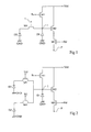
- Figure 1 schematically represents a pixel of a pixel array of an image sensor.
- Each pixel includes a preloading device and a reading device.
- the precharging device consists of a MOS transistor with channel N M1, interposed between a supply rail Vdd and a read node I.
- the gate of the precharge transistor M1 receives a precharge command signal Rs.
- reading consists of the serial connection of two transistors N channel MOS.
- the drain of a first of these transistors reader, hereinafter M2 is connected to the power rail Vdd.
- the source of the second read transistor M3 is connected at the input terminal P of an electronic processing circuit.
- the gate of the first read transistor M2 is connected to the read node I.
- the gate of the second read transistor M3 receives a read signal Rd.
- the cathode of a diode of charge storage D1 is connected to node I.
- the cathode of a photodiode D2 is connected to node I via a charge transfer N channel MOS transistor M4 whose gate receives a charge transfer control signal T.
- the anodes of diode D1 and of photodiode D2 are connected to a reference or ground supply rail of the GND circuit.
- a photodetection cycle begins with a preload phase during which a voltage level of diode D1 is imposed reference. This preload is carried out by passing the precharge transistor M1. Once the preload is completed, the precharge transistor M1 is blocked. Then the system is maintained as it is, all the transistors being blocked. We read then the state at node I, that is to say the state of charge of real reference of diode D1, closing for a very short time instant the second read transistor M3.
- the cycle continues with a transfer to node I photogenerated charges, that is to say created and stored in presence of radiation, in photodiode D2.
- This transfer is carried out by passing the transfer transistor M4.
- the transfer finished, transistor M4 is blocked and photodiode D2 resumes photogenerating and storing charges which will subsequently transferred to node I.
- After the transfer we read the new state of charge of diode D1.
- the signal from output transmitted to terminal P then depends on the pinching of the channel of the first M2 read transistor, which is directly function of the charge stored in the photodiode. Reading finished, transistor M3 is blocked and the cycle starts again with a precharge of the diode D1.
- Figure 2 shows an electrical diagram of a practical implementation of a pixel of an image sensor.
- another photodiode D3 is mounted in parallel to photodiode D2.
- the anode of photodiode D3 is connected to GND ground.
- the cathode of photodiode D3 is connected to node I via a MOS transistor M5 whose gate is controlled by a transfer signal T '.
- Such an electrical diagram therefore consists in putting in common, for two photodiodes D2, D3 of two pixels, the transistors reading M2, M3 and the precharge transistor M1.
- a such structure is called 2.5T pixel since it has 5 MOS transistors for two photodiodes D2, D3, ie "2.5 transistors "by photodiode.
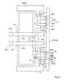
- Figure 3 shows, schematically, a classic example of a 2.5T pixel topology in which the electric circuit of figure 2 is realized by a technology at one level of polycrystalline silicon and three levels of metallization. Other levels of polycrystalline silicon and metallization can be present and used.
- the surfaces delimited by a thin line correspond to active areas of semiconductor substrate, to bands of monocrystalline silicon deposited on the substrate and corresponding to the MOS transistor grids, or to metal strips level 1 or 2.
- the dotted lines indicate portions of polycrystalline silicon strips arranged under portions metal strips or portions of active areas arranged under polycrystalline silicon bands or metallic bands. Although the view is not shown to scale, the relative dimensions of each region are kept so that represent the actual size of the integrated circuit.
- the crosses represent contacts connecting, through the insulating layers located between the metallization levels, bands metallic to active areas or silicon bands polycrystalline or connecting vias, through layers insulation between the metallization levels, strips metallic to other metallic bands.
- An active area 10 corresponds to the photodiodes D2, D3, the transfer transistors M4, M5 and the storage diode D1.
- the active area 10 can be produced according to a technology LOCOS.
- Reference 12 represents a field isolation zone for example in silicon oxide which delimits the active zone 10.
- the gate GM4 of the MOS transistor M4 corresponds to a portion of a polycrystalline silicon strip 14.
- the GM5 grid of the MOS transistor M5 corresponds to a portion of a band of polycrystalline silicon 16.
- the photodiode D2 is produced in the part of the active zone 10 below the grid GM4.
- the photodiode D3 is carried out in the part of active area 10 above the GM5 grid.
- the storage diode D1 is produced between the polycrystalline silicon strips 14, 16.
- a zone active 18 corresponds to the MOS precharge transistor M1.
- a zone active 20 corresponds to the first and second MOS transistors of reading M2, M3.
- the gate GM1 of the MOS transistor M1 corresponds to a portion of a polycrystalline silicon strip 22.
- the grid GM2 of MOS transistor M2 corresponds to a portion of a band of polycrystalline silicon 24.
- the gate GM3 of the MOS transistor of reading M3 corresponds to a portion of a silicon strip polycrystalline 26 which carries the read signal Rd.
- a strip level 1 metallic 28 is connected to the source SM1 of the MOS transistor M1, to the polycrystalline silicon strip 24 and to the active zone 10 between the polycrystalline silicon strips 14, 16.
- a level 1 metal strip 30 is connected to the polycrystalline silicon strip 22 and conducts the signal precharge command Rs.
- a metal strip 32 of level 1, partially covering the strip of polycrystalline silicon 26, plays a role analogous to the role of the metal strip 30 for the row adjacent to the row associated with the 2.5T pixel shown in Figure 3 and located below it.
- the DM1 drains, DM2 of MOS transistors M1, M2 are connected to a strip metallic 33 of level 3 at the supply voltage Vdd.
- the source SM3 of the MOS transistor M3 is connected to a metal strip level 2 connected to the electronic processing system (not shown), only a metal portion 34 of level 1 being represented.
- Level 1 and 2 metal strips (not shown in Figure 3) substantially superimposed on the strips of polycrystalline silicon 14, 16 carry signals from charge transfer T, T 'and are regularly connected to said polycrystalline silicon strips 14, 16 so as to compensate for the resistance of polycrystalline silicon and ensure that all the pixels of a line receive the signals T, T 'at same instant.
- Figure 4 shows a partial section and schematic of the pixel in Figure 3 along line III-III.
- the pixel is produced in a substrate 36 of a first type of conductivity, for example of type P, strongly doped (P +).
- the active zone 10 corresponds to a box 37 of the same type of conductivity than the substrate 36, but more weakly doped.
- a drain region 38 of the opposite conductivity type, for example N, heavily doped (N +) extends between the two gates GM4, GM5 MOS transistors M4, M5.
- Source regions 39, 40 of the opposite type of conductivity are source regions 39, 40 of the opposite type of conductivity.
- Source regions 39, 40 are carried out over a much larger area than the region drain 38 and together with the box 37 underlying the photodiodes D2, D3 junctions.
- P-type regions 41, 42 heavily doped (P +) are connected to the reference potential or to ground via the box 37 and the substrate 36.
- Each photodiode D2, D3 is of the type known as completely depleted and comprises, on the surface of the source region 39, 40, a P 43, 44 type region, shallow and very strongly doped. These regions 43, 44 are in contact with regions 41, 42 and are therefore permanently maintained at the voltage level reference.
- a first insulating layer 45 covers the structure previously described.
- the metal strip 28 at level 1 is connected to the drain region 38 by a contact 47.
- a second insulating layer 49 covers the first insulating layer 45 and the metal strips 28, 30, 32 of the first level of metallization.
- Two metal bands 50, 51 of level 2 extend substantially parallel to the polycrystalline silicon strips 14, 16.
- the insulating layers 45, 49 consist of a transparent insulating material so that the light rays can reach photodiodes D2, D3.
- the absorption of photons leads to the photodiodes D2, D3 the release of electrons that are stored in N-type regions 39, 40
- the absorption of photons at the parts exposed to the light from active areas 18, 20 and polycrystalline silicon strips 22, 24, 26 can also cause in these elements the release of electrons that tend to diffuse to the region 39, 40 of the nearest photodiode D2, D3 and to participate in the charge of the photodiode D2, D3.
- the electrons from active area 20 and silicon strips polycrystalline 24, 26 tend to diffuse mainly towards the photodiode D2, while the electrons from the active area 18 and the polycrystalline silicon strip 22 tend to diffuse mainly towards photodiode D3.
- the exposed surfaces of the active areas 18, 20 are different, and that the exposed surfaces of the polycrystalline silicon strips 22, 24, 26 are also different, one obtains a uneven electron scattering to photodiodes D2, D3 for the same light exposure. This leads to a different charge stored in photodiodes D2, D3 for the same light exposure. Different voltages are then obtained during the transfer of the charges of the photodiodes D2, D3.
- Another possibility is to hide the areas active 18, 20 and the polycrystalline silicon strips 22, 24, 26 not to be exposed to light by a layer metallic with a metallization level higher than level 2.
- the effectiveness of masking obtained may be imperfect given the distance from the mask metallic and photodiodes.
- the present invention aims to obtain a pixel of the type 2.5T does not have the aforementioned drawback.
- a photodetector produced in monolithic form comprising a first active zone of doped monocrystalline silicon corresponding to first and second photodiodes of the same surface, with two MOS transistors of charge transfer and to a storage diode the cathode of each photodiode being connected to the cathode of the diode of storage via one of the MOS transistors of load transfer; a second active silicon zone doped monocrystalline arranged next to the part of the first active area associated with the second photodiode and corresponding to a precharge switch, a first terminal of which is connected to the cathode of the storage diode and of which a second terminal is linked to a reference potential; and a third area active doped monocrystalline silicon arranged next to the part of the first active area associated with the first photodiode and corresponding to two MOS transistors for reading in series, the grid of one of the read transistors being connected to the cathode of the storage diode and the drain or the source of one
- the second and third active areas have substantially surfaces identical.
- the first, second and third active areas are rectangular, the second and third active zones being the same dimensions and substantially aligned at the same distance of one side of the first active area.
- the switch preload is a two-gate MOS transistor parallel.
- the grids of the two read transistors correspond to parts of first and second polycrystalline silicon strips and the two gates of the two-gate MOS transistor correspond to third and fourth strip parts polycrystalline silicon parallels, the sum of the surfaces exposed to the light of the third and fourth bands polycrystalline silicon parallels being substantially equal to the sum of the surfaces exposed to the light of the first and second polycrystalline silicon strips.
- a fifth polycrystalline silicon strip perpendicular to third and fourth parallel bands of polycrystalline silicon, connects the third and fourth parallel strips.
- the photodetector includes a metal strip connected to the fifth polycrystalline silicon strip, said metal strip comprising an extension partially covering the second strip of polycrystalline silicon.
- the charge transfer MOS transistors match to portions of polycrystalline silicon strips which extend between the second and third active zones.
- the principle of the invention consists in fixing the dimensions of the active zones 18, 20 of the charging transistors and reading M1, M2, M3 and the dimensions of the polycrystalline silicon 24, 26 associated so that the surface exposed active area 18 corresponding to the transistor refill M1 is substantially equal to the exposed surface of the active area 20 corresponding to the reading transistors M2, M3 and that the exposed surfaces of the silicon portions polycrystalline associated with the recharge transistor M1 are substantially equal to the sum of the exposed areas of the strips of polycrystalline silicon 24, 26 associated with the transistors of reading M2, M3.
- the present invention provides for using as a transistor of precharge a MOS transistor M1 comprising two gates GM1 ', GM1 "parallel, and called double gate transistor.
- gates GM1 ', GM1 "of the MOS transistor M1 with double gate correspond to parallel portions 53, 54 of strips of polycrystalline silicon connected to a main portion 55 of polycrystalline silicon connected to the metal strip 30.
- This enables an active area 18 of the MOS transistor M1 to be produced, the dimensions are substantially equal to the dimensions of the active zone 20 and to provide exposed surfaces of the portions of polycrystalline silicon 53, 54, 55 substantially equal to the sum of the exposed surfaces of the polycrystalline silicon strips 24, 26.
- the metal strip 32 may include a extension 36 which partially covers the silicon strip polycrystalline 26 associated with the MOS transistor M3 to favor the symmetry of the pixel.
- the gates GM1 ′, GM1 "of MOS transistor M1 are both connected to the band metallic 30 and therefore receive the same control signal from preload Rs. It is however possible to connect the grids GM1 ', GM1 "with two different metal bands so as to control each grid GM1 ', GM1 "by a control signal from specific preload.
- the drains DM1, DM2 of the MOS transistors M1, M2 are connected to the metallic strip 33 of level 3 at the supply voltage Vdd. It is however possible to connect the drains DM1, DM2 to separate metal bands at different voltages.
- the pixel according to the invention being substantially symmetrical, the tensions at the reading node I resulting from the step of discharge of photodiodes D2, D3 are substantially identical for the same light exposure. So we remove all noise undesirable. The same amplification gain can then be used by the electronic processing system for signals from of the two photodiodes.
- the present invention is capable of various variations and modifications that will appear to humans art. So some of the N-channel MOS transistors can be replaced by P-channel transistors.
- the cell realization has been described as implementing one level of polycrystalline silicon and three levels of metallization. It is entirely possible to replace the bands of one or more levels of metallization by a other conductive material.
- the first level of metallization can be replaced by a level two of silicon polycrystalline doped.
Landscapes
- Solid State Image Pick-Up Elements (AREA)
- Transforming Light Signals Into Electric Signals (AREA)
Applications Claiming Priority (2)
| Application Number | Priority Date | Filing Date | Title |
|---|---|---|---|
| FR0211215A FR2844398A1 (fr) | 2002-09-11 | 2002-09-11 | Photodetecteur d'un capteur d'images |
| FR0211215 | 2002-09-11 |
Publications (2)
| Publication Number | Publication Date |
|---|---|
| EP1416538A2 true EP1416538A2 (de) | 2004-05-06 |
| EP1416538A3 EP1416538A3 (de) | 2004-07-28 |
Family
ID=31725985
Family Applications (1)
| Application Number | Title | Priority Date | Filing Date |
|---|---|---|---|
| EP03300114A Withdrawn EP1416538A3 (de) | 2002-09-11 | 2003-09-10 | Photodetektor für einen Bildsensor |
Country Status (3)
| Country | Link |
|---|---|
| US (1) | US7064362B2 (de) |
| EP (1) | EP1416538A3 (de) |
| FR (1) | FR2844398A1 (de) |
Cited By (1)
| Publication number | Priority date | Publication date | Assignee | Title |
|---|---|---|---|---|
| EP1780795A4 (de) * | 2004-07-20 | 2007-08-15 | Fujitsu Ltd | Cmos-bildgeberelement |
Families Citing this family (15)
| Publication number | Priority date | Publication date | Assignee | Title |
|---|---|---|---|---|
| US7542085B2 (en) * | 2003-11-26 | 2009-06-02 | Aptina Imaging Corporation | Image sensor with a capacitive storage node linked to transfer gate |
| US7443437B2 (en) | 2003-11-26 | 2008-10-28 | Micron Technology, Inc. | Image sensor with a gated storage node linked to transfer gate |
| US11282891B2 (en) | 2003-11-26 | 2022-03-22 | Samsung Electronics Co., Ltd. | Image sensor with a gated storage node linked to transfer gate |
| US8072520B2 (en) * | 2004-08-30 | 2011-12-06 | Micron Technology, Inc. | Dual pinned diode pixel with shutter |
| KR100690880B1 (ko) * | 2004-12-16 | 2007-03-09 | 삼성전자주식회사 | 픽셀별 광감도가 균일한 이미지 센서 및 그 제조 방법 |
| US8253214B2 (en) | 2005-06-02 | 2012-08-28 | Omnivision Technologies, Inc. | CMOS shared amplifier pixels with output signal wire below floating diffusion interconnect for reduced floating diffusion capacitance |
| US20070069260A1 (en) * | 2005-09-28 | 2007-03-29 | Eastman Kodak Company | Photodetector structure for improved collection efficiency |
| US7875916B2 (en) * | 2005-09-28 | 2011-01-25 | Eastman Kodak Company | Photodetector and n-layer structure for improved collection efficiency |
| US20080210986A1 (en) * | 2007-03-02 | 2008-09-04 | Micron Technology, Inc | Global shutter pixel with charge storage region |
| JP4350768B2 (ja) | 2007-04-16 | 2009-10-21 | キヤノン株式会社 | 光電変換装置及び撮像装置 |
| US8253810B2 (en) * | 2007-12-05 | 2012-08-28 | Aptina Imaging Corporation | Method, apparatus and system for image stabilization using a single pixel array |
| EP2151828A1 (de) * | 2008-08-04 | 2010-02-10 | STMicroelectronics (Research & Development) Limited | RAM-Speicherschaltung |
| CN103022067A (zh) * | 2012-12-21 | 2013-04-03 | 上海宏力半导体制造有限公司 | Cmos图像传感器的像素单元及cmos图像传感器 |
| AU2018386190A1 (en) * | 2017-12-13 | 2020-06-04 | Magic Leap, Inc. | Global shutter pixel circuit and method for computer vision applications |
| US11462282B2 (en) | 2020-04-01 | 2022-10-04 | Taiwan Semiconductor Manufacturing Co., Ltd. | Semiconductor memory structure |
Family Cites Families (11)
| Publication number | Priority date | Publication date | Assignee | Title |
|---|---|---|---|---|
| US5163179A (en) * | 1991-07-18 | 1992-11-10 | The United States Of America As Represented By The Secretary Of The Air Force | Platinum silicide infrared diode |
| JP2977060B2 (ja) * | 1992-01-29 | 1999-11-10 | オリンパス光学工業株式会社 | 固体撮像装置及びその制御方法 |
| US5614744A (en) * | 1995-08-04 | 1997-03-25 | National Semiconductor Corporation | CMOS-based, low leakage active pixel array with anti-blooming isolation |
| US5587596A (en) * | 1995-09-20 | 1996-12-24 | National Semiconductor Corporation | Single MOS transistor active pixel sensor cell with automatic anti-blooming and wide dynamic range |
| US6160281A (en) | 1997-02-28 | 2000-12-12 | Eastman Kodak Company | Active pixel sensor with inter-pixel function sharing |
| JP4527814B2 (ja) * | 1997-06-11 | 2010-08-18 | 富士通セミコンダクター株式会社 | 半導体装置の製造方法 |
| US6369853B1 (en) * | 1997-11-13 | 2002-04-09 | Foveon, Inc. | Intra-pixel frame storage element, array, and electronic shutter method suitable for electronic still camera applications |
| US6512544B1 (en) * | 1998-06-17 | 2003-01-28 | Foveon, Inc. | Storage pixel sensor and array with compression |
| US6563101B1 (en) * | 2000-01-19 | 2003-05-13 | Barclay J. Tullis | Non-rectilinear sensor arrays for tracking an image |
| US6720594B2 (en) * | 2002-01-07 | 2004-04-13 | Xerox Corporation | Image sensor array with reduced pixel crosstalk |
| US6743652B2 (en) * | 2002-02-01 | 2004-06-01 | Stmicroelectronics, Inc. | Method for making an integrated circuit device including photodiodes |
-
2002
- 2002-09-11 FR FR0211215A patent/FR2844398A1/fr active Pending
-
2003
- 2003-09-09 US US10/658,215 patent/US7064362B2/en not_active Expired - Lifetime
- 2003-09-10 EP EP03300114A patent/EP1416538A3/de not_active Withdrawn
Cited By (2)
| Publication number | Priority date | Publication date | Assignee | Title |
|---|---|---|---|---|
| EP1780795A4 (de) * | 2004-07-20 | 2007-08-15 | Fujitsu Ltd | Cmos-bildgeberelement |
| US8610177B2 (en) | 2004-07-20 | 2013-12-17 | Fujitsu Semiconductor Limited | CMOS imaging device having U-shaped device isolation regions |
Also Published As
| Publication number | Publication date |
|---|---|
| US7064362B2 (en) | 2006-06-20 |
| FR2844398A1 (fr) | 2004-03-12 |
| EP1416538A3 (de) | 2004-07-28 |
| US20040046170A1 (en) | 2004-03-11 |
Similar Documents
| Publication | Publication Date | Title |
|---|---|---|
| EP1883112B1 (de) | Bildsensor, der von der Rückseite beleuchtet wird mit einheitlicher Substrattemperatur | |
| EP1416538A2 (de) | Photodetektor für einen Bildsensor | |
| US8159010B2 (en) | Solid-state image pick-up device and imaging system using the same | |
| CN100499141C (zh) | 固体摄像装置 | |
| EP2216817B1 (de) | Von hinten beleuchteter halbleiter-bildsensor | |
| US8952433B2 (en) | Solid-state image sensor, method of manufacturing the same, and imaging system | |
| FR2820883A1 (fr) | Photodiode a grande capacite | |
| JP2021073688A (ja) | 撮像装置 | |
| US10741602B2 (en) | Back side illuminated CMOS image sensor arrays | |
| WO2011105043A1 (ja) | 固体撮像装置およびカメラ | |
| FR2888989A1 (fr) | Capteur d'images | |
| EP0153251B1 (de) | Bildaufnahmevorrichtung mit stabförmiger multilinearer Ladungsverschiebungsanordnung | |
| EP1873836B1 (de) | Von hinten beleuchtete Bildaufnahmevorrichtung | |
| FR3052297A1 (fr) | Capteur d'image de type a obturation globale | |
| US12046607B2 (en) | Imaging device | |
| US11094734B2 (en) | Imaging device | |
| FR2820882A1 (fr) | Photodetecteur a trois transistors | |
| EP2312832B1 (de) | Pixelschaltung in Bildsensor | |
| FR2846147A1 (fr) | Commande d'une cellule photosensible | |
| FR2934926A1 (fr) | Capteur d'images miniature. | |
| EP1876647A2 (de) | Rückbeleuchteter Bildsensor | |
| FR2910710A1 (fr) | Capteur d'image cmos a photodiode piegee a faible tension d'alimentation | |
| EP1482558A2 (de) | Photodetektoranordnung | |
| TWI789602B (zh) | 影像感測器及捕獲數位電子影像的方法 | |
| FR2824665A1 (fr) | Photodetecteur de type cmos |
Legal Events
| Date | Code | Title | Description |
|---|---|---|---|
| PUAI | Public reference made under article 153(3) epc to a published international application that has entered the european phase |
Free format text: ORIGINAL CODE: 0009012 |
|
| AK | Designated contracting states |
Kind code of ref document: A2 Designated state(s): AT BE BG CH CY CZ DE DK EE ES FI FR GB GR HU IE IT LI LU MC NL PT RO SE SI SK TR |
|
| AX | Request for extension of the european patent |
Extension state: AL LT LV MK |
|
| PUAL | Search report despatched |
Free format text: ORIGINAL CODE: 0009013 |
|
| AK | Designated contracting states |
Kind code of ref document: A3 Designated state(s): AT BE BG CH CY CZ DE DK EE ES FI FR GB GR HU IE IT LI LU MC NL PT RO SE SI SK TR |
|
| AX | Request for extension of the european patent |
Extension state: AL LT LV MK |
|
| RIC1 | Information provided on ipc code assigned before grant |
Ipc: 7H 01L 27/146 A |
|
| 17P | Request for examination filed |
Effective date: 20050126 |
|
| AKX | Designation fees paid |
Designated state(s): DE FR GB IT |
|
| 17Q | First examination report despatched |
Effective date: 20060823 |
|
| STAA | Information on the status of an ep patent application or granted ep patent |
Free format text: STATUS: THE APPLICATION IS DEEMED TO BE WITHDRAWN |
|
| 18D | Application deemed to be withdrawn |
Effective date: 20100402 |