EP1416582A1 - Tragbare elektronische Vorrichtung mit einer elektrischen Verbindung in dem Vorrichtungsgehäuse - Google Patents
Tragbare elektronische Vorrichtung mit einer elektrischen Verbindung in dem Vorrichtungsgehäuse Download PDFInfo
- Publication number
- EP1416582A1 EP1416582A1 EP02079509A EP02079509A EP1416582A1 EP 1416582 A1 EP1416582 A1 EP 1416582A1 EP 02079509 A EP02079509 A EP 02079509A EP 02079509 A EP02079509 A EP 02079509A EP 1416582 A1 EP1416582 A1 EP 1416582A1
- Authority
- EP
- European Patent Office
- Prior art keywords
- electrical
- housing
- module
- contact
- connection means
- Prior art date
- Legal status (The legal status is an assumption and is not a legal conclusion. Google has not performed a legal analysis and makes no representation as to the accuracy of the status listed.)
- Granted
Links
- 230000006835 compression Effects 0.000 claims abstract description 6
- 238000007906 compression Methods 0.000 claims abstract description 6
- 125000006850 spacer group Chemical group 0.000 claims description 14
- 239000004020 conductor Substances 0.000 claims description 10
- 238000004891 communication Methods 0.000 claims description 5
- 239000013013 elastic material Substances 0.000 claims description 4
- 238000007789 sealing Methods 0.000 claims description 4
- 230000001939 inductive effect Effects 0.000 claims description 3
- 238000012423 maintenance Methods 0.000 claims description 2
- 239000000470 constituent Substances 0.000 claims 1
- 230000003993 interaction Effects 0.000 claims 1
- 239000002991 molded plastic Substances 0.000 abstract 1
- 230000000717 retained effect Effects 0.000 abstract 1
- SYSBNFJJSJLZMM-UHFFFAOYSA-N 1,3-dichloro-5-(4-chlorophenyl)benzene Chemical compound C1=CC(Cl)=CC=C1C1=CC(Cl)=CC(Cl)=C1 SYSBNFJJSJLZMM-UHFFFAOYSA-N 0.000 description 12
- 239000000463 material Substances 0.000 description 5
- 230000002093 peripheral effect Effects 0.000 description 4
- 239000000758 substrate Substances 0.000 description 4
- 230000000295 complement effect Effects 0.000 description 3
- 238000004519 manufacturing process Methods 0.000 description 3
- 238000000465 moulding Methods 0.000 description 3
- 230000003014 reinforcing effect Effects 0.000 description 3
- 239000002184 metal Substances 0.000 description 2
- 239000011324 bead Substances 0.000 description 1
- 230000005540 biological transmission Effects 0.000 description 1
- 238000010276 construction Methods 0.000 description 1
- 230000000694 effects Effects 0.000 description 1
- 238000009434 installation Methods 0.000 description 1
- 239000004973 liquid crystal related substance Substances 0.000 description 1
- 238000012986 modification Methods 0.000 description 1
- 230000004048 modification Effects 0.000 description 1
- 230000003647 oxidation Effects 0.000 description 1
- 238000007254 oxidation reaction Methods 0.000 description 1
- 230000002787 reinforcement Effects 0.000 description 1
- 229910052594 sapphire Inorganic materials 0.000 description 1
- 239000010980 sapphire Substances 0.000 description 1
- 238000003466 welding Methods 0.000 description 1
- 238000004804 winding Methods 0.000 description 1
Images


Classifications
-
- H—ELECTRICITY
- H01—ELECTRIC ELEMENTS
- H01Q—ANTENNAS, i.e. RADIO AERIALS
- H01Q1/00—Details of, or arrangements associated with, antennas
- H01Q1/27—Adaptation for use in or on movable bodies
- H01Q1/273—Adaptation for carrying or wearing by persons or animals
-
- A—HUMAN NECESSITIES
- A44—HABERDASHERY; JEWELLERY
- A44C—PERSONAL ADORNMENTS, e.g. JEWELLERY; COINS
- A44C5/00—Bracelets; Wrist-watch straps; Fastenings for bracelets or wrist-watch straps
- A44C5/14—Bracelets; Wrist-watch straps; Fastenings for bracelets or wrist-watch straps characterised by the way of fastening to a wrist-watch or the like
-
- G—PHYSICS
- G04—HOROLOGY
- G04G—ELECTRONIC TIME-PIECES
- G04G17/00—Structural details; Housings
- G04G17/02—Component assemblies
- G04G17/06—Electric connectors, e.g. conductive elastomers
-
- G—PHYSICS
- G04—HOROLOGY
- G04R—RADIO-CONTROLLED TIME-PIECES
- G04R60/00—Constructional details
- G04R60/04—Antennas attached to or integrated in watch bracelets
Definitions
- the present invention relates to a portable device comprising a housing in which is disposed a first electrical module, and a bracelet attached to the housing, the housing comprising an upper part and a lower part which cooperate with each other to mount the housing, a second module electrical connector being associated with the bracelet as well as electrical connection means providing an electrical connection between the first and second electrical modules at through an opening in the housing, the first electrical module comprising at least one electrical contact pad that can be connected to the electrical connection means.
- the present invention relates to such a portable device having means for contacting the connection means electrical with the first electrical module, inside the housing, so removable.
- the term “means of connection” any conductor or set of conductors to ensure electrical connection between two electrical modules.
- electrical module any device intended to supply or receive a power supply and, where appropriate, to transmit or receive an electrical signal.
- the portable electronic device is realized in the form of a portable electronic instrument presented under the form of a wristwatch comprising receiving means, and possibly transmission, radiofrequency type signals.
- the first module Electrical includes electronic circuits for processing electrical signals exchanged with the second electrical module, the latter comprising an antenna.
- European Patent No. 0 631 341 describes an electronic instrument of the type wristwatch having an antenna housed in the bracelet and connected to electronic circuits for processing the signals received by the antenna.
- the circuits electronic processing are arranged inside the instrument housing on a printed circuit board.
- Connection pads are provided on a peripheral region of the circuit board to allow the establishment of an electrical connection between Antenna connection terminals and electronic processing circuits.
- the solution described in this document to ensure the electrical connection between terminals of the antenna and the PCB connection pads is to use fixing screws passing through adapted openings formed in the terminals of the antenna, and screwed into the printed circuit at the connection pads.
- Such an embodiment makes the mounting of the bracelet and the antenna more easier than in the previously described solution to the extent that it is sufficient to plug the electrical conductor in an opening of the housing to make contact electric.
- this solution also has drawbacks, in particular from the point of view of holding in time.
- the spring blade is typically soldered on the printed circuit, which must be done with care to guarantee a sufficient mechanical strength compared to the perpendicular stresses exerted on the blade, once the electrical conductor is placed in support against she.
- the contact surfaces between the blade and the driver are not protected, which can lead to stability problems the electrical connection, in particular because of possible oxidation of the surfaces free metal.
- this solution has a relatively small footprint important and therefore not suitable for the production of an instrument low volume.
- the purpose of the present invention is to improve the devices electronic devices of this kind so as to avoid the aforementioned drawbacks.
- the invention provides a portable device of the type indicated above, characterized by the fact that the mounting of the housing ensures the establishment of a contact electrically, by compression, between said connection means and said stud of contact.
- fastening means are provided for holding together the lower and upper parts of the housing, such as screws for example, the setting implementation of these fixing means to ensure the maintenance of contact between the connection means and the contact pad.
- the second electrical module housed in the bracelet of the portable device can be disconnected from the first module electric by a simple mutual release of the two parts of the housing. Indeed, the discarding the two parts of the housing one of the other can relieve the pressures respectively exerted on the connection means of the second module electrical and on the contact pad of the first electrical module.
- the device portable electronics is an instrument of the wristwatch type presenting means of communication using radio waves.
- electrical conductors are also connect the two terminals of the antenna to the electronic processing circuits, the conductors being arranged through an opening in the housing of the instrument.
- driver regions electrical devices are brought opposite contact pads arranged on a circuit printed bearing electronic processing circuits.
- Means are then provided for compressing these regions of the drivers against the contact pads when mounting the lower and upper case.
- connection means are intended to effect the compression of the connection means against the pads of contact.
- a complete disassembly of the housing is not necessary to disassemble the bracelet and antenna.
- the connection of the antenna to the electronic processing circuits is reliable and presents a good behavior in time.
- the described embodiments relate to a portable electronic device particular as a non-limiting example, namely an instrument of the wristwatch type having at least wave reception features radio frequencies.
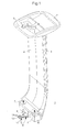
- FIG. 1 represents a preferred embodiment of strand 1 of the bracelet according to the present invention wearing the buckle 2 with its barb 3.
- the bracelet is obtained by molding plastic materials and has an external appearance of conventional type. It can be seen in FIG. 1 that the strand 1 represented has three main building blocks. Strand 1 is obtained by an assembly of two "half-strands" in its thickness, a first internal half-strand 4 and a second half-strand 5. The third component of the strand is a reinforcing element 6, disposed at the end of the strand 1 intended to be connected to the housing of the watch.
- the reinforcing element 6 is made of a plastic material having a higher rigidity important than that of the materials chosen for the manufacture of the half-strands 4 and 5, in order to guarantee the strength of the connection between the housing and the strand 1.
- Holes 7 are provided in the reinforcing element 6 and in the inner half-strand 4 to receive screws fixing (not shown) of the strand 1 to the housing of the watch.
- a pin 8 whose function will be explained later, is arranged at the end of the strand 1 intended to be connected to the housing of the watch.
- the lug 8 is made in one piece with the internal half-strand 4, by a molding of conventional type, and comprises a central hole 9.
- connection means 11 The free end 10 of electrical connection means 11 is apparent, the connecting means leaving the strand 1 through the central hole 9 of the lug 8.
- These means 11 are provided for connecting in particular the terminals of an antenna (visible in Figure 2) disposed between the two half-strands 4 and 5 of the bracelet during their assembly.
- the connection means 11 comprise in particular tracks conductors (not shown) whose ends are shaped into contact 12, the tracks being carried by a flexible substrate 13.
- FIG. 2 is a partial sectional view of strand 1 of a bracelet assembled on the housing 20 of the instrument according to a first embodiment of the invention.
- the representation has been deliberately simplified in order to make the particular characters of the present invention.
- the strand 1 comprises, between its two half-strands 4 and 5, a substrate 13 carrying an antenna 22.
- the type of antenna used is conductive track deposited on a flexible substrate in the form of a spiral.
- the housing 20 of the instrument mainly comprises an upper portion 23, or middle, and a lower part 24, or bottom, the middle part and the bottom being separated by a seal 25 sealing the housing 20.
- the housing is further closed on the above by an ice 26, of conventional type and made for example of plastic or in sapphire according to the desired level of range.
- the middle part 23 has an opening 27 on its side in which is inserted the lug 8 of the strand 1 of the bracelet.
- the transverse dimensions of the spigot 8 are preferably chosen slightly higher than those of the opening 27.
- the lug 8 is frictionally housed in the opening 27 and itself ensures the tightness of the housing at the level of the opening.
- This construction detail advantageously allows to do without the use of an additional seal at this location for perform the introduction of the connection means 11 of the antenna 22 inside the housing 20. It is also possible to provide beads of material (not shown) molded with the lug 8 to ensure sealing at the opening 27.
- the reinforcement element 6 has a thin portion 28 extending inside the central hole 9 of the lug 8, supported against the means of connection 11 of the antenna, thereby ensuring a certain rigidity to the pin 8 possible deformations could be harmful from the point of view of the tightness of the instrument. It can also be noted that the deformations possible pin 8 are likely to damage the antenna 22, which is avoided right here.
- the peripheral portion 29 of the bottom 24 has a shape complementary to that of the end of the inner half-strand 4 intended to be fixed to the housing 20 of the instrument.
- the middle part 23 has a shape substantially complementary to that of the part of the strand 1 intended to be arranged opposite the middle part 23.
- the strand 1 is wedged between the middle part 23 and the bottom 24.
- screws are provided for fixing the strand 1 to the housing 20. It may be noted that, according to a preferred alternative, these screws also pass through holes (not shown) formed in the bottom 24, at its peripheral portion 29, to allow the mounting of the housing 20.
- the housing 20 contains electronic circuits 30 allowing in particular command display means, shown schematically in Figure 2 by a screen to liquid crystal 31, or LCD screen.
- the electronic circuits 30 can furthermore include means to perform a variety of additional functions, such as watchmaking movement of conventional type for example, to allow a display the current time.
- a power source shown with the reference 48 in Figure 5 to feed the various components of the instrument according to the invention.
- the electronic circuits 30 are further electrically connected to a first electrical module 32 comprising, in the illustrated example, electronic circuits for processing the signals received by the antenna 22.
- the first electrical module comprises contact pads 33 intended to be brought into contact with the contact 12 of the antenna 22.
- the middle part 23 comprises a flange 34 having a shoulder 35 against which the screen LCD 31 is disposed in support.
- the electrical module 32 is disposed in support against the LCD screen 31, either directly or via elements additional (not shown), possibly of the spacer type.
- you can provide for peripheral regions of certain components arranged in the 23 strike up against regions of the latter, as is the case for the electrical module 32 in FIG.
- feet can be provided, of which only one 36 is shown schematically in FIG. 2, in particular to position the circuits 30.
- the electronic circuits 30 are preferably supported by a printed circuit board (not shown) having through-holes different locations, provided to cooperate with the positioning feet, such a structure being known.
- the foot 36 has a second function in addition to its conventional positioning function electronic circuits. Indeed, it is apparent from Figure 2 that when the housing 20 of the portable device is mounted, the end 10 of the connection means 11 is located compressed by the foot 36 against the contact pads 33 of the first electrical module 32.
- the simple assembly of the upper parts causes the establishment of an electrical connection between a first and a second electrical module, that is to say here circuits 32 signal processing electronics and an antenna 22.
- Means of this specific electrical connection such as a weld or a screws are not necessary contrary to what is known from the prior art.
- the step of setting up such means for establishing the connection electrical, when mounting the housing is advantageously removed.
- An additional advantage of the structure according to the present invention comes from the fact that the first electrical module 32 and the lug 8 of the bracelet, so the end 10 of the connection means 11, are positioned relative to a single and even reference to the middle part 23. Therefore, good reliability in the arrangement of these components can be obtained during assembly, to the extent where it does not depend on tolerances on the dimensions or positioning of others housing components 20.
- the foot 36 it is preferably performed at the same time that the bottom by molding plastic material, or metal.
- a additional element whose face intended to come into contact with the end 10 of connection means 11 is substantially flat and covers at least one surface equal to that of the contact pads 33.
- this additional element is in such a way that the aforementioned face can be deformed to guarantee a good quality of contact between the connection means 11 and the pads of contact 33.
- FIG. 3 represents in perspective a part of the portable device according to a second preferred embodiment of the present invention.
- FIG. 1 shows the strand 1 previously described in connection with FIG. also shown in view from below a middle part 23 similar to that described in relationship with Figure 2 and, in which is visible only part of the components provided in the housing 20.
- the strand 1 is ready to be put in place on the middle 23.
- the middle part 23 comprises a plurality of guiding surfaces 37 for cooperating with surfaces of the end of the strand 1 intended to be fixed to the housing 20. It can be seen in particular that the middle part 23 has a surface 38 of complementary section to about half that of the lug 8 and thus ensuring a radial guide function for the strand 1.
- FIG. 3 furthermore appears, facing the guide surface 38, the opening 27 of the middle part 23 intended to receive the lug 8 of the strand 1 to allow the introduction of the connection means 11 of the antenna 22 in the housing 20 of the portable device.
- all the electronic circuits of the portable device is arranged on a printed circuit board 39, or PCB ("Printed Circuit Board "), which is the case in particular of the first electrical module 32.
- PCB printed Circuit Board
- said circuits may include circuits of the watchmaking type to enable the wearable device to present hourly features in addition of its specific functionalities related to the means of communication by waves radio.
- Figures 4a to 4c show better the particular details related to the connection of the two electrical modules, namely the antenna and the circuits electronic processing of electrical signals received by said antenna.
- FIG. 4a represents a view similar to that of FIG. part has been enlarged, the strand 1 of the bracelet being closer to the middle part 23.
- a spacer 40 has been added, in support on the PCB 39, its main function being to present a bearing surface 41, for subsequent mounting steps, located in a plane substantially parallel to the plane of PCB 39 and at a distance greater than the height of the electronic component the highest carried by the PCB.
- the spacer 40 has a housing 42 whose function will be exposed more far, in connection with the description of Figures 4b and 4c.
- the transverse dimensions of the housing 42 are substantially greater than the dimensions of all the contact pads 33 so as to leave these accessible through the housing.
- the end 10 of the connection means It has four contact pads 43.
- the second electrical module housed in the strand 1 may have a plurality of functions.
- two 12 of the contact pads 43 are used to connect the terminals of the antenna 22 to the electronic circuits arranged in the housing 20, while that the two remaining contact pads 43 can be used to connect a other component.
- a charging coil (not shown) further on the substrate 13, the ends of which are connected to the remaining contact pads 43.
- FIGS. 4b and 4c show the introduction of a buffer 44 substantially parallelepiped in the housing 42 of the spacer 40, after having disposed the strand 1 against the middle part 23, so after having introduced the connection means 11 to inside the housing 20.
- the buffer 44 preferably made of an elastic material such as rubber, for example, is simply deposited inside the housing 42, in superposition of the end 10 of the connection means 11.
- the latter has a thickness slightly greater than that of the spacer 40.
- the upper face 45 of the buffer that is the one that is not in contact with the connection means 11, is projecting relative to the bearing surface 41 defined by the spacer 40.
- FIG. 5 is a diagrammatic section showing the device that has just been described, once the bottom 24 is mounted on the middle part 23, allows better understand the function of buffer 44.
- the general structure shown in the figure 5 is similar to that shown in Figure 2, which is why the description of common elements between these two figures will not be repeated for Figure 5.
- the PCB 39 carrying electronic components, whose first electrical module 32 is here electronic circuits for processing the signals received by the antenna 22.
- An intermediate spacing element 46 is disposed between the LCD screen 31 and PCB 39 to ensure sufficient height between these two elements and allow the arrangement of the components, such as the schematized module 47, on the PCB 39 in the intermediate space thus defined.
- connection means 11 introduced in the housing 20 through the opening 27 of the middle part, are arranged between the element 46 and the spacer 40, so that the contact pads 43 are arranged opposite the corresponding contact pads 33 of the PCB 39.
- electric conduction tracks (not shown) are further provided on the PCB 39 to electrically connect the contact pads 33 with the first module electric 32.
- the power source used is a battery 48 large diameter. It can be seen that the battery 48 is arranged directly with its first face against the bottom 24 of the housing 20, while its second face is supported on the spacer 40.
- the second face of the battery 48 is also supported on the face 45 buffer, so as to compress the latter and to ensure the electrical contact between the contact pads 43 the connection means 11 and the contact pads 33 of PCB 39.
- the PCB 39 and the contact pads 33 are located substantially in the same plane as the opening 27, such that the end 10 of the connection means 11 does not require to be bent when inserted next to the contact pads 33. In this case, it can easily do without the rounding 49 described above.
- the portable device according to the The present invention advantageously makes it possible to establish an electrical connection between at least two electrical modules without imposing the need to provide a step specific for establishing said connection, such as a step of screwing or welding, when mounting the device.
- the portable device according to the present invention is also capable of transmitting radio waves via the antenna 22.
Landscapes
- Physics & Mathematics (AREA)
- General Physics & Mathematics (AREA)
- Electric Clocks (AREA)
- Telephone Set Structure (AREA)
Priority Applications (4)
| Application Number | Priority Date | Filing Date | Title |
|---|---|---|---|
| EP02079509A EP1416582B1 (de) | 2002-10-28 | 2002-10-28 | Tragbare elektronische Vorrichtung mit einer elektrischen Verbindung in dem Vorrichtungsgehäuse |
| AT02079509T ATE399375T1 (de) | 2002-10-28 | 2002-10-28 | Tragbare elektronische vorrichtung mit einer elektrischen verbindung in dem vorrichtungsgehäuse |
| DE60227260T DE60227260D1 (de) | 2002-10-28 | 2002-10-28 | Tragbare elektronische Vorrichtung mit einer elektrischen Verbindung in dem Vorrichtungsgehäuse |
| US10/693,893 US6854978B2 (en) | 2002-10-28 | 2003-10-28 | Portable electronic device including means for establishing an electrical connection inside a case of said device |
Applications Claiming Priority (1)
| Application Number | Priority Date | Filing Date | Title |
|---|---|---|---|
| EP02079509A EP1416582B1 (de) | 2002-10-28 | 2002-10-28 | Tragbare elektronische Vorrichtung mit einer elektrischen Verbindung in dem Vorrichtungsgehäuse |
Publications (2)
| Publication Number | Publication Date |
|---|---|
| EP1416582A1 true EP1416582A1 (de) | 2004-05-06 |
| EP1416582B1 EP1416582B1 (de) | 2008-06-25 |
Family
ID=32088039
Family Applications (1)
| Application Number | Title | Priority Date | Filing Date |
|---|---|---|---|
| EP02079509A Expired - Lifetime EP1416582B1 (de) | 2002-10-28 | 2002-10-28 | Tragbare elektronische Vorrichtung mit einer elektrischen Verbindung in dem Vorrichtungsgehäuse |
Country Status (4)
| Country | Link |
|---|---|
| US (1) | US6854978B2 (de) |
| EP (1) | EP1416582B1 (de) |
| AT (1) | ATE399375T1 (de) |
| DE (1) | DE60227260D1 (de) |
Cited By (2)
| Publication number | Priority date | Publication date | Assignee | Title |
|---|---|---|---|---|
| EP2741152A1 (de) * | 2012-12-06 | 2014-06-11 | ETA SA Manufacture Horlogère Suisse | Armbanduhr, die mit einem elektrischen Steckverbinder ausgestattet ist |
| EP3432087A1 (de) * | 2017-07-21 | 2019-01-23 | ETA SA Manufacture Horlogère Suisse | Befestigungsvorrichtung |
Families Citing this family (31)
| Publication number | Priority date | Publication date | Assignee | Title |
|---|---|---|---|---|
| CH713523B1 (fr) * | 2001-11-26 | 2018-09-14 | Ebauchesfabrik Eta Ag | Objet électronique portatif tel qu'une pièce d'horlogerie susceptible d'être porté au poignet. |
| EP1398676A1 (de) * | 2002-09-10 | 2004-03-17 | The Swatch Group Management Services AG | Uhr mit einem elektronischen Modul, zum Informationspeichern, die in dem Boden angeordnet ist |
| US7096048B2 (en) * | 2003-04-01 | 2006-08-22 | Sanders Donald T | Portable communications device |
| EP1491973A1 (de) * | 2003-06-25 | 2004-12-29 | The Swatch Group Management Services AG | Schliessenarmband mit elektrischer Anschlussvorrichtung |
| EP1513032A1 (de) * | 2003-09-02 | 2005-03-09 | The Swatch Group Management Services AG | Gerät mit einem elektronischen Modul, zum Informationspeichern, und elektronischer Modul, der mit diesem Gerät vereinbar ist |
| DE60306382T2 (de) * | 2003-09-23 | 2007-05-03 | Asulab S.A. | Adapter für ein tragbares elektronisches Gerät und Übertragungssystem zwischen diesen Bauteilen |
| JP2007085821A (ja) * | 2005-09-21 | 2007-04-05 | Citizen Watch Co Ltd | 腕時計型機器 |
| US7382328B2 (en) * | 2006-03-22 | 2008-06-03 | Radio Systems Corporation | Antenna enclosed within an animal training apparatus |
| JP5190061B2 (ja) | 2007-08-30 | 2013-04-24 | シャープ株式会社 | 超解像光記録媒体、光記録媒体再生装置、光記録媒体再生装置の制御方法、光記録媒体再生装置制御プログラム、並びにそれを記録したコンピュータ読み取り可能な記録媒体 |
| ITVR20080025U1 (it) * | 2008-10-27 | 2010-04-28 | Hawai Italia Srl | Ardiglio particolarmente conformato e fibbia comprendente tale ardiglio |
| US8059491B1 (en) * | 2009-06-26 | 2011-11-15 | Laura Hennings-Kampa | Rescue-facilitating communicating wrist watch |
| US20120315776A1 (en) * | 2011-06-08 | 2012-12-13 | Wei-Jia Liang | Connector assembly |
| US9362776B2 (en) * | 2012-11-27 | 2016-06-07 | Qualcomm Incorporated | Wireless charging systems and methods |
| US9977461B2 (en) | 2013-03-01 | 2018-05-22 | Rufus Labs, Inc. | Wearable mobile device |
| EP2813907B1 (de) * | 2013-06-11 | 2018-08-01 | LG Electronics, Inc. | Uhrenartiges mobiles Terminal |
| KR102052972B1 (ko) * | 2013-06-11 | 2019-12-06 | 엘지전자 주식회사 | 와치형 이동단말기 |
| USD730348S1 (en) | 2014-01-09 | 2015-05-26 | Rufus Armor, Llc | Wearable mobile device |
| US9445633B2 (en) * | 2014-09-30 | 2016-09-20 | Apple Inc. | Portable electronic device connector |
| US9720376B2 (en) * | 2014-11-18 | 2017-08-01 | Sony Corporation | Band type electronic device and substrate arrangement method |
| US10498158B2 (en) * | 2015-03-31 | 2019-12-03 | Superior Communications, Inc. | Watch strap battery |
| EP3101508B1 (de) * | 2015-05-22 | 2020-04-08 | Lg Electronics Inc. | Tragbare intelligente vorrichtung |
| US20160363957A1 (en) | 2015-06-09 | 2016-12-15 | Christian Stroetmann | Wearable computer with electronic strap and attachment therefor |
| CN105305019B (zh) * | 2015-09-29 | 2018-06-26 | 联想(北京)有限公司 | 一种穿戴式电子设备 |
| US9461386B1 (en) * | 2015-10-09 | 2016-10-04 | Pebble Technology, Corp. | Spring pin electrical connector |
| KR102680702B1 (ko) * | 2016-06-14 | 2024-07-03 | 삼성전자주식회사 | 스트랩 및 이를 포함하는 전자 장치 |
| JP6384738B2 (ja) * | 2016-07-07 | 2018-09-05 | カシオ計算機株式会社 | モジュールおよび時計 |
| US10058148B1 (en) * | 2016-09-21 | 2018-08-28 | Apple Inc. | Attachment mechanism architectures for a watch band |
| US10058149B1 (en) * | 2016-09-21 | 2018-08-28 | Apple Inc. | Attachment mechanism architectures for a watch band |
| TWI622899B (zh) * | 2016-09-30 | 2018-05-01 | 仁寶電腦工業股份有限公司 | 穿戴式裝置及其模組化功能組件 |
| KR102514256B1 (ko) * | 2017-09-28 | 2023-03-27 | 삼성전자주식회사 | 밴드를 포함하는 웨어러블 전자 장치 |
| US20240106270A1 (en) * | 2022-09-23 | 2024-03-28 | Apple Inc. | Inductive coil assemblies for electronic devices and accessories |
Citations (4)
| Publication number | Priority date | Publication date | Assignee | Title |
|---|---|---|---|---|
| US4947179A (en) * | 1988-05-27 | 1990-08-07 | Junghans Uhren Gmbh | Antenna for a radio controlled timepiece |
| US5168281A (en) * | 1990-05-16 | 1992-12-01 | Seiko Epson Corporation | Antenna connection device for electronic equipment |
| EP0631341A1 (de) * | 1993-06-28 | 1994-12-28 | Seiko Instruments Inc. | Elektrische Vorrichtung mit einem Verdrahtungskreis in einem Armband |
| EP0867968A2 (de) * | 1997-03-25 | 1998-09-30 | Seiko Epson Corporation | Kommunikationsgerät zur Montage am Handgelenk |
Family Cites Families (41)
| Publication number | Priority date | Publication date | Assignee | Title |
|---|---|---|---|---|
| JPS5426044Y2 (de) * | 1977-02-26 | 1979-08-29 | ||
| US5265265A (en) * | 1990-02-09 | 1993-11-23 | Seiko Epson Corporation | Wristwatch radio communication device having an improved noise shielding structure |
| US5450091A (en) * | 1988-08-05 | 1995-09-12 | Seiko Epson Corporation | Variable size antenna device having resonance frequency compensation |
| US5135694A (en) * | 1989-11-10 | 1992-08-04 | Seiko Epson Corporation | Electronic device wristband |
| US5179733A (en) * | 1990-04-23 | 1993-01-12 | Seiko Epson Corporation | Wristwatch band with radio antenna |
| US5189431A (en) * | 1990-10-22 | 1993-02-23 | Motorola, Imc. | Removable antenna coupling on a wrist watch pager |
| US5465098A (en) * | 1991-11-05 | 1995-11-07 | Seiko Epson Corporation | Antenna apparatus for transceiver |
| US5589840A (en) * | 1991-11-05 | 1996-12-31 | Seiko Epson Corporation | Wrist-type wireless instrument and antenna apparatus |
| US5280296A (en) * | 1992-04-29 | 1994-01-18 | Motorola, Inc. | Antenna system for a wrist carried selective call receiver |
| KR100298001B1 (ko) * | 1993-03-17 | 2001-10-24 | 구사마 사부로 | 팔찌형안테나장치및그장치를구비한무선기 |
| US5742256A (en) * | 1993-05-07 | 1998-04-21 | Seiko Epson Corporation | Wristband having embedded electrically conductive members for a wrist-mountable type electronic device |
| US5615179A (en) * | 1993-05-07 | 1997-03-25 | Seiko Epson Corporation | Electronic apparatus with fitting band |
| GB2280065B (en) * | 1993-07-16 | 1997-05-14 | Nec Corp | Wristwatch-type selective calling receiver |
| US5499292A (en) * | 1994-05-06 | 1996-03-12 | At&T Corp. | On hook/off hook mechanism for wrist telephone |
| US5564082A (en) * | 1994-05-06 | 1996-10-08 | At&T Corp. | Diversity antenna for a wrist telephone |
| US5986566A (en) * | 1994-08-18 | 1999-11-16 | Oi Denki Co., Ltd. | Wrist band antenna |
| DE69523037T2 (de) * | 1995-05-05 | 2002-10-24 | Eta S.A. Fabriques D'ebauches, Grenchen/Granges | Antennenstruktur für eine Uhr |
| DE69520351T2 (de) * | 1995-05-05 | 2001-10-11 | Eta S.A. Fabriques D'ebauches, Grenchen/Granges | Antennenstruktur für eine Uhr |
| US5886669A (en) * | 1995-05-10 | 1999-03-23 | Casio Computer Co., Ltd. | Antenna for use with a portable radio apparatus |
| KR19990028636A (ko) * | 1995-07-05 | 1999-04-15 | 모토로라, 인크 | 컨포멀 전원 장치 |
| FR2739200B1 (fr) * | 1995-09-26 | 1997-10-31 | Asulab Sa | Piece d'horlogerie comportant une antenne |
| JPH09307329A (ja) * | 1996-05-14 | 1997-11-28 | Casio Comput Co Ltd | アンテナ及びその製造方法並びにアンテナを備えた電 子機器又は電子時計 |
| WO1997048025A1 (de) * | 1996-06-10 | 1997-12-18 | Asulab S.A. | Tragbare präzisionsuhr mit zusatzfunktionen |
| JPH10163268A (ja) * | 1996-12-03 | 1998-06-19 | Seiko Epson Corp | 半導体装置の実装構造、およびそれを用いた通信装置 |
| US5864061A (en) * | 1997-02-05 | 1999-01-26 | Dilz, Jr.; Albert E. | Miniature sports radar speed measuring device |
| SE511277C2 (sv) * | 1998-01-05 | 1999-09-06 | Ericsson Telefon Ab L M | Antennanslutning |
| FR2775809B1 (fr) * | 1998-03-09 | 2002-06-14 | Finaluxe | Bracelet comportant des moyens pour son identification |
| DE19853899C2 (de) * | 1998-11-23 | 2001-11-22 | Horst Spanyar | Vorrichtung zur elektrischen Verbindung eines Handys mit einer Tastatur |
| KR100313144B1 (ko) * | 1998-11-27 | 2001-11-07 | 윤종용 | 와치 타입 휴대용 무선단말기 |
| CA2292194C (en) * | 1998-12-22 | 2010-02-16 | Eta Sa Fabriques D'ebauches | Wristwatch with capacitive coupling |
| JP3106206B1 (ja) * | 1999-05-27 | 2000-11-06 | 新生化学工業株式会社 | 情報記憶媒体の携帯具 |
| DE19926271C2 (de) * | 1999-06-09 | 2002-09-26 | Junghans Uhren Gmbh | Funkarmbanduhr |
| US6192253B1 (en) * | 1999-10-06 | 2001-02-20 | Motorola, Inc. | Wrist-carried radiotelephone |
| US6366250B1 (en) * | 1999-12-09 | 2002-04-02 | Sirf Technology, Inc. | Wrist mounted wireless instrument and antenna apparatus |
| JP2001186584A (ja) * | 1999-12-27 | 2001-07-06 | Casio Comput Co Ltd | 外部接続用アダプタおよび電子機器 |
| SG101434A1 (en) * | 1999-12-29 | 2004-01-30 | Asulab Sa | Wristwatch provided with an antenna |
| JP4042340B2 (ja) * | 2000-05-17 | 2008-02-06 | カシオ計算機株式会社 | 情報機器 |
| JP2002136311A (ja) * | 2000-08-23 | 2002-05-14 | Seiko Instruments Inc | 腕情報機器 |
| EP1315051A1 (de) | 2001-11-26 | 2003-05-28 | ETA SA Manufacture Horlogère Suisse | Kleines elektronisches Objekt, das am Arm getragen werden kann |
| EP1315234A1 (de) | 2001-11-26 | 2003-05-28 | Eta SA Fabriques d'Ebauches | VHF-Empfangsantenne integriert in das Armband einer tragbaren elektronischen Vorrichtung |
| EP1315265A1 (de) | 2001-11-27 | 2003-05-28 | ETA SA Manufacture Horlogère Suisse | Tragbares Armbandgerät mit elektrischen Verbindungsmitteln |
-
2002
- 2002-10-28 AT AT02079509T patent/ATE399375T1/de not_active IP Right Cessation
- 2002-10-28 EP EP02079509A patent/EP1416582B1/de not_active Expired - Lifetime
- 2002-10-28 DE DE60227260T patent/DE60227260D1/de not_active Expired - Lifetime
-
2003
- 2003-10-28 US US10/693,893 patent/US6854978B2/en not_active Expired - Lifetime
Patent Citations (4)
| Publication number | Priority date | Publication date | Assignee | Title |
|---|---|---|---|---|
| US4947179A (en) * | 1988-05-27 | 1990-08-07 | Junghans Uhren Gmbh | Antenna for a radio controlled timepiece |
| US5168281A (en) * | 1990-05-16 | 1992-12-01 | Seiko Epson Corporation | Antenna connection device for electronic equipment |
| EP0631341A1 (de) * | 1993-06-28 | 1994-12-28 | Seiko Instruments Inc. | Elektrische Vorrichtung mit einem Verdrahtungskreis in einem Armband |
| EP0867968A2 (de) * | 1997-03-25 | 1998-09-30 | Seiko Epson Corporation | Kommunikationsgerät zur Montage am Handgelenk |
Cited By (5)
| Publication number | Priority date | Publication date | Assignee | Title |
|---|---|---|---|---|
| EP2741152A1 (de) * | 2012-12-06 | 2014-06-11 | ETA SA Manufacture Horlogère Suisse | Armbanduhr, die mit einem elektrischen Steckverbinder ausgestattet ist |
| US8976628B2 (en) | 2012-12-06 | 2015-03-10 | Eta Sa Manufacture Horlogere Suisse | Wristwatch provided with an electrical connector |
| EP3432087A1 (de) * | 2017-07-21 | 2019-01-23 | ETA SA Manufacture Horlogère Suisse | Befestigungsvorrichtung |
| JP2019023628A (ja) * | 2017-07-21 | 2019-02-14 | ウーテーアー・エス・アー・マニファクチュール・オロロジェール・スイス | 固定デバイス |
| US10499714B2 (en) | 2017-07-21 | 2019-12-10 | Eta Sa Manufacture Horlogere Suisse | Fixing device |
Also Published As
| Publication number | Publication date |
|---|---|
| ATE399375T1 (de) | 2008-07-15 |
| US20040084200A1 (en) | 2004-05-06 |
| EP1416582B1 (de) | 2008-06-25 |
| US6854978B2 (en) | 2005-02-15 |
| DE60227260D1 (de) | 2008-08-07 |
Similar Documents
| Publication | Publication Date | Title |
|---|---|---|
| EP1416582B1 (de) | Tragbare elektronische Vorrichtung mit einer elektrischen Verbindung in dem Vorrichtungsgehäuse | |
| EP2741152B1 (de) | Armbanduhr, die mit einem elektrischen Steckverbinder ausgestattet ist | |
| EP1513221A1 (de) | Tragbares Armbandgerät mit elektrischem Verbindungselement durchs Gehäuse und Verfahren zur Montage des Verbindungselements | |
| EP1315234A1 (de) | VHF-Empfangsantenne integriert in das Armband einer tragbaren elektronischen Vorrichtung | |
| EP1513220B1 (de) | Patch-Antenne integriert in einer Armbanduhr | |
| EP1143573A1 (de) | Koaxialer Verbinder | |
| EP0074006A1 (de) | Elektronische Gelenkarmbanduhr sowie Verfahren zur Herstellung einer Dichtung für diese Gelenkarmbanduhr | |
| FR2677816A1 (fr) | Connecteur coaxial pour le raccordement d'un cable coaxial a une carte imprimee de circuit electronique. | |
| EP3457222B1 (de) | Armbanduhrengehäuse mit beweglichen bandanstössen | |
| EP1381119A1 (de) | Elektrische Steckverbindungsanordnung | |
| FR2869499A1 (fr) | Cadre de blindage pour un ensemble de protection vis-a-vis des frequences radio | |
| FR2762150A1 (fr) | Connecteur d'entree/sortie pour dispositif portable de communication et procede de montage dudit connecteur | |
| EP0186804B1 (de) | Am Armgelenk zu tragende elektronische Vorrichtung | |
| FR2687856A1 (fr) | Connecteur en elastomere electriquement conducteur. | |
| EP1519457B1 (de) | Adapter für ein tragbares elektronisches Gerät und Übertragungssystem zwischen diesen Bauteilen | |
| FR2485220A1 (fr) | Bati et bloc modulaires pour instruments horaires | |
| EP1593317B1 (de) | Armband, insbesondere für eine Uhr, mit einem eingearbeiteten elektrisch leitenden Element | |
| FR2629662A1 (fr) | Capsule electroacoustique a bobine rapportee | |
| EP2745661A2 (de) | Elektrische verbindungsvorrichtung, anordnung mit einer solchen vorrichtung und elektronikplatine sowie verfahren zum elektrischen anschluss einer elektronikplatine | |
| FR2560059A1 (fr) | Jouet produisant des sons | |
| EP1513222B1 (de) | Tragbares Armbandgerät mit elektrischem Verbindungselement durchs Gehäuse und Verfahren zur Montage des Verbindungselements | |
| EP3054359A1 (de) | Montagevorrichtung einer elektrischen Energiequelle | |
| EP3811471B1 (de) | Elektrisches verbindungssystem mit einer primären verbindungsvorrichtung und einer sekundären verbindungsvorrichtung | |
| EP1538697B1 (de) | Tragbares Armbandgerät mit einer elektrischen Verbindungsvorrichtung durch das Gehäuse | |
| FR2662863A1 (fr) | Dispositif connecteur adaptateur de terminaison. |
Legal Events
| Date | Code | Title | Description |
|---|---|---|---|
| PUAI | Public reference made under article 153(3) epc to a published international application that has entered the european phase |
Free format text: ORIGINAL CODE: 0009012 |
|
| AK | Designated contracting states |
Kind code of ref document: A1 Designated state(s): AT BE BG CH CY CZ DE DK EE ES FI FR GB GR IE IT LI LU MC NL PT SE SK TR |
|
| AX | Request for extension of the european patent |
Extension state: AL LT LV MK RO SI |
|
| 17P | Request for examination filed |
Effective date: 20041108 |
|
| AKX | Designation fees paid |
Designated state(s): AT BE BG CH CY CZ DE DK EE ES FI FR GB GR IE IT LI LU MC NL PT SE SK TR |
|
| 17Q | First examination report despatched |
Effective date: 20070308 |
|
| GRAP | Despatch of communication of intention to grant a patent |
Free format text: ORIGINAL CODE: EPIDOSNIGR1 |
|
| GRAS | Grant fee paid |
Free format text: ORIGINAL CODE: EPIDOSNIGR3 |
|
| GRAA | (expected) grant |
Free format text: ORIGINAL CODE: 0009210 |
|
| AK | Designated contracting states |
Kind code of ref document: B1 Designated state(s): AT BE BG CH CY CZ DE DK EE ES FI FR GB GR IE IT LI LU MC NL PT SE SK TR |
|
| REG | Reference to a national code |
Ref country code: GB Ref legal event code: FG4D Free format text: NOT ENGLISH |
|
| REG | Reference to a national code |
Ref country code: CH Ref legal event code: EP |
|
| REF | Corresponds to: |
Ref document number: 60227260 Country of ref document: DE Date of ref document: 20080807 Kind code of ref document: P |
|
| REG | Reference to a national code |
Ref country code: IE Ref legal event code: FG4D Free format text: LANGUAGE OF EP DOCUMENT: FRENCH |
|
| REG | Reference to a national code |
Ref country code: CH Ref legal event code: NV Representative=s name: ICB INGENIEURS CONSEILS EN BREVETS SA |
|
| PG25 | Lapsed in a contracting state [announced via postgrant information from national office to epo] |
Ref country code: FI Free format text: LAPSE BECAUSE OF FAILURE TO SUBMIT A TRANSLATION OF THE DESCRIPTION OR TO PAY THE FEE WITHIN THE PRESCRIBED TIME-LIMIT Effective date: 20080625 |
|
| PG25 | Lapsed in a contracting state [announced via postgrant information from national office to epo] |
Ref country code: AT Free format text: LAPSE BECAUSE OF FAILURE TO SUBMIT A TRANSLATION OF THE DESCRIPTION OR TO PAY THE FEE WITHIN THE PRESCRIBED TIME-LIMIT Effective date: 20080625 Ref country code: NL Free format text: LAPSE BECAUSE OF FAILURE TO SUBMIT A TRANSLATION OF THE DESCRIPTION OR TO PAY THE FEE WITHIN THE PRESCRIBED TIME-LIMIT Effective date: 20080625 |
|
| NLV1 | Nl: lapsed or annulled due to failure to fulfill the requirements of art. 29p and 29m of the patents act | ||
| PG25 | Lapsed in a contracting state [announced via postgrant information from national office to epo] |
Ref country code: CZ Free format text: LAPSE BECAUSE OF FAILURE TO SUBMIT A TRANSLATION OF THE DESCRIPTION OR TO PAY THE FEE WITHIN THE PRESCRIBED TIME-LIMIT Effective date: 20080625 Ref country code: PT Free format text: LAPSE BECAUSE OF FAILURE TO SUBMIT A TRANSLATION OF THE DESCRIPTION OR TO PAY THE FEE WITHIN THE PRESCRIBED TIME-LIMIT Effective date: 20081125 Ref country code: SE Free format text: LAPSE BECAUSE OF FAILURE TO SUBMIT A TRANSLATION OF THE DESCRIPTION OR TO PAY THE FEE WITHIN THE PRESCRIBED TIME-LIMIT Effective date: 20080925 Ref country code: ES Free format text: LAPSE BECAUSE OF FAILURE TO SUBMIT A TRANSLATION OF THE DESCRIPTION OR TO PAY THE FEE WITHIN THE PRESCRIBED TIME-LIMIT Effective date: 20081006 |
|
| REG | Reference to a national code |
Ref country code: IE Ref legal event code: FD4D |
|
| PG25 | Lapsed in a contracting state [announced via postgrant information from national office to epo] |
Ref country code: SK Free format text: LAPSE BECAUSE OF FAILURE TO SUBMIT A TRANSLATION OF THE DESCRIPTION OR TO PAY THE FEE WITHIN THE PRESCRIBED TIME-LIMIT Effective date: 20080625 |
|
| BERE | Be: lapsed |
Owner name: ETA SA MANUFACTURE HORLOGERE SUISSE Effective date: 20081031 |
|
| PG25 | Lapsed in a contracting state [announced via postgrant information from national office to epo] |
Ref country code: DK Free format text: LAPSE BECAUSE OF FAILURE TO SUBMIT A TRANSLATION OF THE DESCRIPTION OR TO PAY THE FEE WITHIN THE PRESCRIBED TIME-LIMIT Effective date: 20080625 Ref country code: BG Free format text: LAPSE BECAUSE OF FAILURE TO SUBMIT A TRANSLATION OF THE DESCRIPTION OR TO PAY THE FEE WITHIN THE PRESCRIBED TIME-LIMIT Effective date: 20080925 Ref country code: IE Free format text: LAPSE BECAUSE OF FAILURE TO SUBMIT A TRANSLATION OF THE DESCRIPTION OR TO PAY THE FEE WITHIN THE PRESCRIBED TIME-LIMIT Effective date: 20080625 Ref country code: EE Free format text: LAPSE BECAUSE OF FAILURE TO SUBMIT A TRANSLATION OF THE DESCRIPTION OR TO PAY THE FEE WITHIN THE PRESCRIBED TIME-LIMIT Effective date: 20080625 |
|
| PLBE | No opposition filed within time limit |
Free format text: ORIGINAL CODE: 0009261 |
|
| STAA | Information on the status of an ep patent application or granted ep patent |
Free format text: STATUS: NO OPPOSITION FILED WITHIN TIME LIMIT |
|
| PG25 | Lapsed in a contracting state [announced via postgrant information from national office to epo] |
Ref country code: MC Free format text: LAPSE BECAUSE OF NON-PAYMENT OF DUE FEES Effective date: 20081031 |
|
| 26N | No opposition filed |
Effective date: 20090326 |
|
| PG25 | Lapsed in a contracting state [announced via postgrant information from national office to epo] |
Ref country code: IT Free format text: LAPSE BECAUSE OF FAILURE TO SUBMIT A TRANSLATION OF THE DESCRIPTION OR TO PAY THE FEE WITHIN THE PRESCRIBED TIME-LIMIT Effective date: 20080625 |
|
| PG25 | Lapsed in a contracting state [announced via postgrant information from national office to epo] |
Ref country code: BE Free format text: LAPSE BECAUSE OF NON-PAYMENT OF DUE FEES Effective date: 20081031 |
|
| PGFP | Annual fee paid to national office [announced via postgrant information from national office to epo] |
Ref country code: GB Payment date: 20090928 Year of fee payment: 8 |
|
| PG25 | Lapsed in a contracting state [announced via postgrant information from national office to epo] |
Ref country code: CY Free format text: LAPSE BECAUSE OF FAILURE TO SUBMIT A TRANSLATION OF THE DESCRIPTION OR TO PAY THE FEE WITHIN THE PRESCRIBED TIME-LIMIT Effective date: 20080625 Ref country code: LU Free format text: LAPSE BECAUSE OF NON-PAYMENT OF DUE FEES Effective date: 20081028 |
|
| PG25 | Lapsed in a contracting state [announced via postgrant information from national office to epo] |
Ref country code: TR Free format text: LAPSE BECAUSE OF FAILURE TO SUBMIT A TRANSLATION OF THE DESCRIPTION OR TO PAY THE FEE WITHIN THE PRESCRIBED TIME-LIMIT Effective date: 20080625 |
|
| PG25 | Lapsed in a contracting state [announced via postgrant information from national office to epo] |
Ref country code: GR Free format text: LAPSE BECAUSE OF FAILURE TO SUBMIT A TRANSLATION OF THE DESCRIPTION OR TO PAY THE FEE WITHIN THE PRESCRIBED TIME-LIMIT Effective date: 20080926 |
|
| GBPC | Gb: european patent ceased through non-payment of renewal fee |
Effective date: 20101028 |
|
| PG25 | Lapsed in a contracting state [announced via postgrant information from national office to epo] |
Ref country code: GB Free format text: LAPSE BECAUSE OF NON-PAYMENT OF DUE FEES Effective date: 20101028 |
|
| REG | Reference to a national code |
Ref country code: FR Ref legal event code: PLFP Year of fee payment: 14 |
|
| REG | Reference to a national code |
Ref country code: FR Ref legal event code: PLFP Year of fee payment: 15 |
|
| REG | Reference to a national code |
Ref country code: FR Ref legal event code: PLFP Year of fee payment: 16 |
|
| REG | Reference to a national code |
Ref country code: FR Ref legal event code: PLFP Year of fee payment: 17 |
|
| PGFP | Annual fee paid to national office [announced via postgrant information from national office to epo] |
Ref country code: FR Payment date: 20200917 Year of fee payment: 19 |
|
| PGFP | Annual fee paid to national office [announced via postgrant information from national office to epo] |
Ref country code: DE Payment date: 20200917 Year of fee payment: 19 |
|
| PGFP | Annual fee paid to national office [announced via postgrant information from national office to epo] |
Ref country code: CH Payment date: 20210921 Year of fee payment: 20 |
|
| REG | Reference to a national code |
Ref country code: DE Ref legal event code: R119 Ref document number: 60227260 Country of ref document: DE |
|
| PG25 | Lapsed in a contracting state [announced via postgrant information from national office to epo] |
Ref country code: DE Free format text: LAPSE BECAUSE OF NON-PAYMENT OF DUE FEES Effective date: 20220503 |
|
| PG25 | Lapsed in a contracting state [announced via postgrant information from national office to epo] |
Ref country code: FR Free format text: LAPSE BECAUSE OF NON-PAYMENT OF DUE FEES Effective date: 20211031 |
|
| REG | Reference to a national code |
Ref country code: CH Ref legal event code: PL |