EP1417151B1 - Procede de fabrication de microstructures en silicium poreux en suspension et leur mise en oeuvre dans des capteurs de gaz - Google Patents
Procede de fabrication de microstructures en silicium poreux en suspension et leur mise en oeuvre dans des capteurs de gaz Download PDFInfo
- Publication number
- EP1417151B1 EP1417151B1 EP02712117A EP02712117A EP1417151B1 EP 1417151 B1 EP1417151 B1 EP 1417151B1 EP 02712117 A EP02712117 A EP 02712117A EP 02712117 A EP02712117 A EP 02712117A EP 1417151 B1 EP1417151 B1 EP 1417151B1
- Authority
- EP
- European Patent Office
- Prior art keywords
- porous silicon
- membrane
- suspended
- silicon
- membranes
- Prior art date
- Legal status (The legal status is an assumption and is not a legal conclusion. Google has not performed a legal analysis and makes no representation as to the accuracy of the status listed.)
- Expired - Lifetime
Links
Images



Classifications
-
- H—ELECTRICITY
- H05—ELECTRIC TECHNIQUES NOT OTHERWISE PROVIDED FOR
- H05B—ELECTRIC HEATING; ELECTRIC LIGHT SOURCES NOT OTHERWISE PROVIDED FOR; CIRCUIT ARRANGEMENTS FOR ELECTRIC LIGHT SOURCES, IN GENERAL
- H05B3/00—Ohmic-resistance heating
- H05B3/20—Heating elements having extended surface area substantially in a two-dimensional [2D] plane, e.g. plate-heater
- H05B3/22—Heating elements having extended surface area substantially in a two-dimensional [2D] plane, e.g. plate-heater non-flexible
- H05B3/26—Heating elements having extended surface area substantially in a two-dimensional [2D] plane, e.g. plate-heater non-flexible heating conductor mounted on insulating base
- H05B3/265—Heating elements having extended surface area substantially in a two-dimensional [2D] plane, e.g. plate-heater non-flexible heating conductor mounted on insulating base the insulating base being an inorganic material, e.g. ceramic
-
- B—PERFORMING OPERATIONS; TRANSPORTING
- B81—MICROSTRUCTURAL TECHNOLOGY
- B81C—PROCESSES OR APPARATUS SPECIALLY ADAPTED FOR THE MANUFACTURE OR TREATMENT OF MICROSTRUCTURAL DEVICES OR SYSTEMS
- B81C1/00—Manufacture or treatment of devices or systems in or on a substrate
- B81C1/00642—Manufacture or treatment of devices or systems in or on a substrate for improving the physical properties of a device
- B81C1/0065—Mechanical properties
- B81C1/00682—Treatments for improving mechanical properties, not provided for in B81C1/00658 - B81C1/0065
-
- B—PERFORMING OPERATIONS; TRANSPORTING
- B81—MICROSTRUCTURAL TECHNOLOGY
- B81C—PROCESSES OR APPARATUS SPECIALLY ADAPTED FOR THE MANUFACTURE OR TREATMENT OF MICROSTRUCTURAL DEVICES OR SYSTEMS
- B81C1/00—Manufacture or treatment of devices or systems in or on a substrate
- B81C1/00642—Manufacture or treatment of devices or systems in or on a substrate for improving the physical properties of a device
- B81C1/0069—Thermal properties, e.g. improve thermal insulation
-
- G—PHYSICS
- G01—MEASURING; TESTING
- G01F—MEASURING VOLUME, VOLUME FLOW, MASS FLOW OR LIQUID LEVEL; METERING BY VOLUME
- G01F1/00—Measuring the volume flow or mass flow of fluid or fluent solid material wherein the fluid passes through a meter in a continuous flow
- G01F1/68—Measuring the volume flow or mass flow of fluid or fluent solid material wherein the fluid passes through a meter in a continuous flow by using thermal effects
- G01F1/684—Structural arrangements; Mounting of elements, e.g. in relation to fluid flow
- G01F1/6845—Micromachined devices
-
- B—PERFORMING OPERATIONS; TRANSPORTING
- B81—MICROSTRUCTURAL TECHNOLOGY
- B81B—MICROSTRUCTURAL DEVICES OR SYSTEMS, e.g. MICROMECHANICAL DEVICES
- B81B2201/00—Specific applications of microelectromechanical systems
- B81B2201/02—Sensors
- B81B2201/0278—Temperature sensors
-
- B—PERFORMING OPERATIONS; TRANSPORTING
- B81—MICROSTRUCTURAL TECHNOLOGY
- B81B—MICROSTRUCTURAL DEVICES OR SYSTEMS, e.g. MICROMECHANICAL DEVICES
- B81B2203/00—Basic microelectromechanical structures
- B81B2203/01—Suspended structures, i.e. structures allowing a movement
- B81B2203/0109—Bridges
-
- B—PERFORMING OPERATIONS; TRANSPORTING
- B81—MICROSTRUCTURAL TECHNOLOGY
- B81B—MICROSTRUCTURAL DEVICES OR SYSTEMS, e.g. MICROMECHANICAL DEVICES
- B81B2203/00—Basic microelectromechanical structures
- B81B2203/01—Suspended structures, i.e. structures allowing a movement
- B81B2203/0118—Cantilevers
-
- B—PERFORMING OPERATIONS; TRANSPORTING
- B81—MICROSTRUCTURAL TECHNOLOGY
- B81C—PROCESSES OR APPARATUS SPECIALLY ADAPTED FOR THE MANUFACTURE OR TREATMENT OF MICROSTRUCTURAL DEVICES OR SYSTEMS
- B81C2201/00—Manufacture or treatment of microstructural devices or systems
- B81C2201/01—Manufacture or treatment of microstructural devices or systems in or on a substrate
- B81C2201/0101—Shaping material; Structuring the bulk substrate or layers on the substrate; Film patterning
- B81C2201/0111—Bulk micromachining
- B81C2201/0115—Porous silicon
-
- G—PHYSICS
- G01—MEASURING; TESTING
- G01N—INVESTIGATING OR ANALYSING MATERIALS BY DETERMINING THEIR CHEMICAL OR PHYSICAL PROPERTIES
- G01N27/00—Investigating or analysing materials by the use of electric, electrochemical, or magnetic means
- G01N27/02—Investigating or analysing materials by the use of electric, electrochemical, or magnetic means by investigating impedance
- G01N27/04—Investigating or analysing materials by the use of electric, electrochemical, or magnetic means by investigating impedance by investigating resistance
- G01N27/12—Investigating or analysing materials by the use of electric, electrochemical, or magnetic means by investigating impedance by investigating resistance of a solid body in dependence upon absorption of a fluid; of a solid body in dependence upon reaction with a fluid, for detecting components in the fluid
-
- G—PHYSICS
- G01—MEASURING; TESTING
- G01N—INVESTIGATING OR ANALYSING MATERIALS BY DETERMINING THEIR CHEMICAL OR PHYSICAL PROPERTIES
- G01N27/00—Investigating or analysing materials by the use of electric, electrochemical, or magnetic means
- G01N27/02—Investigating or analysing materials by the use of electric, electrochemical, or magnetic means by investigating impedance
- G01N27/04—Investigating or analysing materials by the use of electric, electrochemical, or magnetic means by investigating impedance by investigating resistance
- G01N27/14—Investigating or analysing materials by the use of electric, electrochemical, or magnetic means by investigating impedance by investigating resistance of an electrically-heated body in dependence upon change of temperature
- G01N27/16—Investigating or analysing materials by the use of electric, electrochemical, or magnetic means by investigating impedance by investigating resistance of an electrically-heated body in dependence upon change of temperature caused by burning or catalytic oxidation of surrounding material to be tested, e.g. of gas
-
- G—PHYSICS
- G01—MEASURING; TESTING
- G01N—INVESTIGATING OR ANALYSING MATERIALS BY DETERMINING THEIR CHEMICAL OR PHYSICAL PROPERTIES
- G01N27/00—Investigating or analysing materials by the use of electric, electrochemical, or magnetic means
- G01N27/02—Investigating or analysing materials by the use of electric, electrochemical, or magnetic means by investigating impedance
- G01N27/04—Investigating or analysing materials by the use of electric, electrochemical, or magnetic means by investigating impedance by investigating resistance
- G01N27/14—Investigating or analysing materials by the use of electric, electrochemical, or magnetic means by investigating impedance by investigating resistance of an electrically-heated body in dependence upon change of temperature
- G01N27/18—Investigating or analysing materials by the use of electric, electrochemical, or magnetic means by investigating impedance by investigating resistance of an electrically-heated body in dependence upon change of temperature caused by changes in the thermal conductivity of a surrounding material to be tested
Definitions
- This invention relates to a method of fabricating suspended porous silicon membranes and to devices made employing this method.
- the closed-type membrane is formed by means of anisotropic (crystallographic) etching of silicon from the back side of the wafer.
- Wet etchants like KOH and EDP are typically used. Appropriate etch stops for these etchants are silicon nitride, silicon oxide or Boron- doped silicon.
- the first which is more popular, uses silicon oxide and/or silicon nitride as membrane and insulation materials to obtain membranes of typical thickness between 1 and 2 ⁇ m [(a) G. Sberveglieri et al. Microsyst. Technolog., p.183, 1997, (b) J. Gardner, Sens. Actuators B 26/27, p.
- the second method which has been applied recently, uses nitrided porous silicon of thickness between 25 and 30 ⁇ m (Maccagnani et al., Proceed. of the 13 th European Conference on Solid-State Transducers, The Netherlands 1999) that can be obtained by silicon anodization and subsequent nitridation. Silicon oxide, silicon nitride and nitrided porous silicon all possess low thermal conductivities and can provide good thermal isolation between the heated active area and the membrane rim.
- the suspended-type membrane is completely processed from the front-side. Therefore, the suspended membrane is often said to be more compatible with CMOS processing (Gaitan et al., US Patent. 5,464,966).
- the suspended membrane is either formed by anisotropic wet etching with KOH or EDP from the front side or by sacrificial etching of oxide layers. Sacrificial etching of porous silicon is another possibility to obtain suspended membranes (Nassiopoulou et al., Application No PCT/GR97/00040, published by WIPO 12/11/1998 as WO 98/50763. Suspended polycrystalline and monocrystalline membranes have been fabricated using this technique by Kaltsas and Nassiopoulou [( ⁇ ) G.
- suspended membranes are generally preferred compared to the closed-type membranes. The reason is that the thermal losses from the suspended-type membrane are minimized, since they occur only through the supporting beams of the membrane, compared to the closed membrane where thermal losses occur along its periphery.
- Highly porous silicon (with porosity ⁇ 65%) has very good thermal properties similarly to silicon oxide. In sensor applications, it has been used in two ways: as a material for local thermal isolation on a silicon substrate [(a) Nassiopoulou et al., Application No PCT/GR97/00040 published by WIPO 12/11/1998, (b) G. as WO 98/50763 Kaltsas and A.G Nassiopoulou, Sens. Actuators A 76, p. 133, 1999] and as sacrificial layer for the formation of suspended membranes. Recently, nitrided porous silicon membranes were fabricated using backside etching. Maccagnani et al. (Maccagnani Proc.
- the release of single-crystal silicon structures from the substrate through the front side of the wafer can be achieved by means of a combined directional and isotropic silicon dry etch if the structures are protected on the sides by a Si-etching selective mask such as for example SiO 2 (F. Ayazi, et. al. JMEMS 9(3), p. 288, 2000).
- the released structure is made of porous Si, which simplifies extremely the process : The high selectivity of the used isotropic Si etching process with respect to porous Si makes unnecessary any protection of the structure to be released.
- MACCAGNAMI P ET AL "Thick porous silicon thermo-insulating membranes for gas sensor applications” SENSORS AND MATERIALS, 1999, MY, JAPAN, Vol. 11, no. 3, pages 131-147, ISSN: 0914-4935 discloses the fabrication of a closed type porous silicon membrane in contact with the silicon substrate along its perimeter. During formation of the membrane, silicon etching is performed from the back side of the wafer in order to form a mono-crystalline silicon membrane and, subsequently, anodization is performed to form the porous silicon membrane.
- KOLEV S D ET AL "Thermal modeling of a porous silicon-based pellisor-type catalytic flammable gas sensor with two supporting beams" MICOELECTRONICS JOURNAL, MACKINTOSH PUBLICATIONS LTD., LUTON, GB, vol. 31, no. 5, May 2000 (2000-05), pages 339-342, ISSN: 0026-2692 discloses a gas sensor including a membrane of silicon nitride suspended by two beams. An n-silicon heater and a porous silicon layer, both rectangular in shape, are provided on the membrane.
- BARATTO ET AL. "Front-side micromachined porous silicon nitrogen dioxide gas sensor" Thin Solid Films, vol. 391, 16 June 2001 (2001-06-16), pages 261-264, discloses a gas sensor with a closed porous silicon membrane suspended by a silicon nitride layer and a SiC layer. An air gap below the porous silicon membrane is obtained by electropolishing.
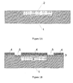
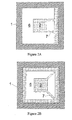
- Figs. 1A through 1C are schematic drawings illustrating the fabrication process of suspended Porous Silicon membranes.
- the base material (1) doped monocrystalline or polycrystalline silicon is used.
- the dopant concentration in the substrate can be either n type or p type with concentrations greater that 10 14 cm -2 .
- Porous silicon (2) is formed in predefined areas of the said substrate.
- Various masking techniques have been used for the local formation of porous silicon. These techniques include deposition and patterning of various layers such as Si 3 N 4 , SiO 2 , SiGe, SiC, polycrystalline silicon and combination of them as well as ion implantation techniques.
- the masking material or method for the local patterning of porous silicon is not a limiting factor for the method described in this invention.
- Fig. 1A shows the substrate (1) and the defined Porous Silicon area (2).
- the mask for the local formation of Porous Silicon may consist of a silicon dioxide layer and a polysilicon layer, according to one of the embodiments of the present invention.
- an insulating layer (3) is deposited on top of porous silicon (Fig 1B).
- the insulating layer (3) can be SiO 2 or Si 3 N 4 or any combination of them.
- photoresist (4) is deposited on top of the wafer and etch windows (5) are opened using standard photolithography techniques.
- the etch windows (5) are placed at the periphery of the porous silicon membrane (2) or at predefined places inside the membrane (Fig 1B).
- the removal of the insulating layers (3) and the mask, that is used for the local formation of porous silicon (2) can be achieved either by wet or dry etching techniques.
- the etch windows (5) extend down to the silicon substrate (1) adjacent to the porous silicon membrane (2).
- the silicon material from underneath the porous structure is removed by a combination of anisotropic / isotropic dry etching processes.
- Fig. 1C shows a cross section schematic of the released Porous Silicon membrane where the cavity (6) formed under the porous silicon (2) is shown.
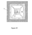
- Figs. 2A to Fig 2C show various top view designs of suspended Porous Silicon structures, where we can see the silicon substrate (1), the porous silicon membrane (2) and the porous silicon supporting beams (7). The membrane is suspended over the cavity (6).
- One of the key parameters for the successful implementation of the methodology that is described in the present invention is the optimization of dry etching conditions.
- Various processes can be used provided that the etching conditions are selected in such a way that the process is highly selective to silicon etching compared to Porous Silicon etching.
- an F-rich gas as sulfur hexafluoride is used which has a flow of between 100-300 seem and a processing pressure between 1 and 10 Pa.
- the plasma generation preferably takes place with a high frequency supply (13.56 MHz) at outputs between 500 W and 2000 W.
- a low substrate voltage for ion acceleration is supplied to the substrate electrode.
- the substrate voltage is preferably between 30 and 60 V.
- etch rate depends on the dimensions of the etch windows. This phenomenon has been observed in the past in high aspect ratio Si etching and is known as RIE lag. Experiments that were performed by the inventors demonstrated that this influence exists also for lateral etching of Si. However this influence of the dimension of the etch window on the Si etch rate does not impose any constraints on the method that is described in the present invention. On the contrary, by carefully designing the position and the dimensions of the etch windows, it is possible to benefit from this dependence and release selectively suspended microstructures of certain shapes, and sizes.
- Another key parameter for the successful implementation of the proposed methodology is the optimization of mechanical properties of the characteristics of the Porous Silicon layer. It is obvious that the structural characteristics of the Porous Silicon membranes (porosity, thickness, pore size) and the, subsequent thermal treatment have to be optimized according to the design and geometrical characteristics of the layer. With the aid of the methodology proposed in the present invention, suspended Porous Silicon membranes have been formed with thickness ranging from few nm to several micrometers and with size up to several millimeters.
- a calorimetric type gas sensor is fabricated.
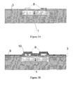
- an insulating layer (3) is deposited, as shown in Fig. 3A.
- the insulating layer can be either SiO 2 , or Si 3 N 4 or any combination of them. However, it is desirable to use an insulating material with very low thermal conductivity.
- a heater (8) is formed on top of the said insulating layer (3) (Fig. 3A). The heater is made either of doped polycrystalline silicon or any conducting layer or layer combination, as for example Pt/Ti.
- An insulating layer 9 is then deposited on top of the heater (8) (Fig: 3B). The deposition method of the said insulating layer (9) depends on the nature of the heater.
- the insulating layer can be SiO 2 deposited by LPCVD or LTO techniques.
- a catalytic layer (10) is then deposited on top of the said insulating layer (9) (Fig. 3B).
- the selection of the catalytic material can be made over a vast range of materials, such as Pt, Pd for example.
- the choice of the catalytic material will depend on the properties of the gas to be detected
- the only limitation for the catalytic material, according to the methodology described in the present invention, is to remain unaffected by the processes that follow, and particularly by the removal of the photoresist, which can be performed either by using wet techniques (for example by exposure to organic solvents such as acetone) or dry etching techniques (for example O 2 plasma).
- the patterning of the catalytic layer can be achieved either by the lift-off technique or by standard photolithography techniques combined with wet etching, if needed.
- the temperature change from the heat that is generated or absorbed from the catalytic reaction of the gases on the surface of the catalytic layer (10) can be detected, either by the heated resistor (8) or by a second resistor, a sensing resistor, that is implemented in the device (not shown on Fig. 3).
- integrated thermopiles can be used to detect the temperature changes due to the catalytic reaction,
- thermocouples in the form of a plurality of thermocouples may be provided the contact of each of the thermocouples being located on the suspended porous silicon membrane and the other being located on the silicon substrate.
- Fig. 3C shows a cross section schematic drawing of the gas sensor, where we can see the cavity (6) that is formed under the porous silicon (2).
- Fig. 4 shows a plan view drawing of the device, where we can see the silicon substrate (1), the porous silicon membrane (2), the porous silicon supporting beams (7) and an indicative design of the heater (8).
- a conductometric type gas sensor is fabricated.
- the fabrication process for the formation of the porous silicon area (2) and the heater (8) is similar to the process described above (Fig 5A).
- conductive electrodes (11) are deposited and patterned (Fig. 5B).
- the catalytic material (10) is deposited on top of the electrodes (Fig. 5B).
- the choice of the catalytic material depends on the gas to be detected and can be selected by a large range of materials (SnO 2 for example) or any material whose 50 electrical characteristics depend on the ambient gas.
- the release of the porous silicon membrane is performed in the way described previously.
- Fig. 5C shows a cross sectional schematic drawing of the gas sensor after the release of the porous silicon membrane, where we can see the cavity (6) formed under the porous silicon membrane (2).
- a thermal conductivity sensor can be formed by depositing a Pt resistor (12) on top of a Porous Silicon membrane (2) suspended over the cavity (6), as illustrated in Fig. 6.
- An insulating layer (3) may exist between the resistor and the Porous Silicon membrane (2).
- the dimensions of the suspended porous silicon membrane (2) can be changed in order to modulate the response time of the sensor.
- porous silicon membranes Although the description we have provided up to now has focused on the release of porous silicon membranes, it is possible to use the method described in this invention for the release of suspended membranes that are made of silicon oxide, nitride or any stack of these materials, due to the high selectivity of dry etching of Si with respect to SiO 2 /Si 3 N 4 . With a slightly modified fabrication process, polycrystalline silicon membranes can be also released.
Landscapes
- Engineering & Computer Science (AREA)
- Physics & Mathematics (AREA)
- Manufacturing & Machinery (AREA)
- Microelectronics & Electronic Packaging (AREA)
- General Physics & Mathematics (AREA)
- Fluid Mechanics (AREA)
- Mechanical Engineering (AREA)
- Chemical & Material Sciences (AREA)
- Ceramic Engineering (AREA)
- Thermal Sciences (AREA)
- Micromachines (AREA)
- Pressure Sensors (AREA)
- Investigating Or Analyzing Materials By The Use Of Electric Means (AREA)
- Ceramic Products (AREA)
- Investigating Or Analyzing Materials By The Use Of Fluid Adsorption Or Reactions (AREA)
Claims (8)
- Procédé de micro-usinage de substrat de silicium sur la face avant pour la fabrication de membranes suspendues à base de silicium poreux et en forme de ponts ou de cantilevers comprenant
la formation d'une membrane de silicium poreux (2) sur au moins une région prédéfinie d'un substrat de silicium (1);
la définition des fenêtres de gravure (5) autour des bords ou dans la membrane de silicium poreux (2) en utilisant la photolithographie standard; ensuite la gravure sélective du substrat de silicium (1) de la face avant sous
la membrane du silicium poreux (2) en utilisant des techniques de gravure sèche afin de dégager la membrane de silicium poreux (2) et de former une cavité (6) sous la membrane de silicium poreux (2). - Procédé de micro-usinage de silicium sur la face avant comme revendique' dans la reendication 1, où la piste d'une couche conductrice (8) est formée au dessus de la membrane du silicium poreux (2).
- Capteur de gaz comprenant un substrat de silicium (1), une membrane de silicium poreux (2) suspendue au dessus d'une cavité (6) formée sur le substrat de silicium (1), afin de fournir une isolation thermique locale et une piste d'une couche conductrice (8) fournie au dessus de la membrane suspendue (2), caracterisee en ce que la membrane (2) est suspendue d'un ou plusieurs supports à silicium poreux (7) qui sont formés intégralement avec la membrane.
- Capteur de gaz comme revendique' dans la revendication 3 où une couche électriquement isolatrice (3) est fournie au dessus de la couche conductrice (8), un matériel catalytique (10) est fourni au dessus de la couche isolatrice (3) et un capteur thermique qui détecte les changements de température lorsque le gaz d'atmosphère réagit avec le matériel catalytique (10).
- Capteur de gaz comme revendique' dans la revendication 4 où le capteur thermique est une résistance de Pt.
- Capteur de gaz comme revendique' dans la revendication 4 où le capteur thermique inclut une multitude de thermocouples, dont un contact de chaque thermocouple est localisé sur la membrane suspendue de silicium poreux (2) et l'autre est localisé sur le substrat de silicium (1),
- Capteur de gaz comme revendique' dans la revendication 3 où une couche électriquement isolatrice (3) est fournie au dessus de la couche conductrice (8), des électrodes métalliques (11) sont fournis au dessus de la couche isolatrice (3) et un matériel catalytique (10) est fourni au dessus des électrodes (11), la résistivité du matériau catalytique (10) étant dépendante du gaz d'atmosphère.
- Capteur de gaz comme revendique' dans la revendication 3 où la piste de la couche conductrice (8) est une résistance de Pt.
Applications Claiming Priority (3)
| Application Number | Priority Date | Filing Date | Title |
|---|---|---|---|
| GR20010100378A GR1004040B (el) | 2001-07-31 | 2001-07-31 | Μεθοδος για την κατασκευη αιωρουμενων μεμβρανων πορωδους πυριτιου και εφαρμογης της σε αισθητηρες αεριων |
| GR2001100378 | 2001-07-31 | ||
| PCT/GR2002/000008 WO2003011747A1 (fr) | 2001-07-31 | 2002-02-18 | Procede de fabrication de microstructures en silicium poreux en suspension et leur mise en oeuvre dans des capteurs de gaz |
Publications (3)
| Publication Number | Publication Date |
|---|---|
| EP1417151A1 EP1417151A1 (fr) | 2004-05-12 |
| EP1417151B1 true EP1417151B1 (fr) | 2007-01-03 |
| EP1417151B9 EP1417151B9 (fr) | 2007-08-08 |
Family
ID=10944796
Family Applications (1)
| Application Number | Title | Priority Date | Filing Date |
|---|---|---|---|
| EP02712117A Expired - Lifetime EP1417151B9 (fr) | 2001-07-31 | 2002-02-18 | Procede de fabrication de microstructures en silicium poreux en suspension et leur mise en oeuvre dans des capteurs de gaz |
Country Status (8)
| Country | Link |
|---|---|
| US (1) | US20040195096A1 (fr) |
| EP (1) | EP1417151B9 (fr) |
| JP (1) | JP2005502480A (fr) |
| CN (1) | CN1538934A (fr) |
| AT (1) | ATE350333T1 (fr) |
| DE (1) | DE60217359D1 (fr) |
| GR (1) | GR1004040B (fr) |
| WO (1) | WO2003011747A1 (fr) |
Cited By (1)
| Publication number | Priority date | Publication date | Assignee | Title |
|---|---|---|---|---|
| EP4576930A1 (fr) * | 2023-12-21 | 2025-06-25 | Infineon Technologies AG | Dispositif de chauffage mems et capteur de fluide mems |
Families Citing this family (78)
| Publication number | Priority date | Publication date | Assignee | Title |
|---|---|---|---|---|
| DE10032579B4 (de) * | 2000-07-05 | 2020-07-02 | Robert Bosch Gmbh | Verfahren zur Herstellung eines Halbleiterbauelements sowie ein nach dem Verfahren hergestelltes Halbleiterbauelement |
| US20080044939A1 (en) * | 2002-01-24 | 2008-02-21 | Nassiopoulou Androula G | Low power silicon thermal sensors and microfluidic devices based on the use of porous sealed air cavity technology or microchannel technology |
| GR1004106B (el) * | 2002-01-24 | 2003-01-13 | Εκεφε "Δημοκριτος" Ινστιτουτο Μικροηλεκτρονικης | Ολοκληρωμενοι θερμικοι αισθητηρες πυριτιου χαμηλης ισχυος και διαταξεις μικρο-ροης βασισμενοι στην χρηση τεχνολογιας κοιλοτητας αερα σφραγισμενης με μεμβρανη πορωδους πυριτιου ή τεχνολογιας μικρο-καναλιων |
| DE10260859B4 (de) * | 2002-12-23 | 2008-12-04 | Robert Bosch Gmbh | Strukturkörper mit einem porösen Bereich und dessen Verwendung sowie Verfahren zur Einstellung der Wärmeleitfähigkeit eines porösen Bereiches |
| WO2004077073A1 (fr) * | 2003-02-24 | 2004-09-10 | University Of Florida | Accelerometre monolithique integre a trois axes, micro-usine |
| US7026184B2 (en) * | 2003-02-26 | 2006-04-11 | Carnegie Mellon University | Method of fabricating microstructures and devices made therefrom |
| FR2854277B1 (fr) | 2003-04-24 | 2005-08-05 | Commissariat Energie Atomique | Detecteur thermique de rayonnement electromagnetique a structure alveolee |
| US7762719B2 (en) * | 2004-04-20 | 2010-07-27 | California Institute Of Technology | Microscale calorimeter |
| CN1294074C (zh) * | 2004-04-29 | 2007-01-10 | 上海交通大学 | 金属薄膜微桥的制造方法及其力学特性测试方法 |
| EP1915598B1 (fr) * | 2005-08-17 | 2011-03-09 | Panasonic Electric Works Co., Ltd. | Unité de capteur infrarouge et son procédé de fabrication |
| JP4899715B2 (ja) * | 2005-08-17 | 2012-03-21 | パナソニック電工株式会社 | 赤外線センサユニットの製造方法 |
| JP4801396B2 (ja) * | 2005-09-01 | 2011-10-26 | 敏嗣 植田 | ガスセンサ及びガスセンサの製造方法 |
| EP1772717B1 (fr) * | 2005-10-04 | 2011-05-11 | Sensirion Holding AG | Capteur de pression ou capteur de gaz et méthode de mesure utilisant des nanopores |
| CN100348953C (zh) * | 2005-12-19 | 2007-11-14 | 浙江大学 | 一种测热式微型流量传感器 |
| DE102006028435A1 (de) | 2006-06-21 | 2007-12-27 | Robert Bosch Gmbh | Sensor und Verfahren zu seiner Herstellung |
| JP4997039B2 (ja) * | 2007-09-20 | 2012-08-08 | アズビル株式会社 | フローセンサ |
| US7928343B2 (en) * | 2007-12-04 | 2011-04-19 | The Board Of Trustees Of The University Of Illinois | Microcantilever heater-thermometer with integrated temperature-compensated strain sensor |
| WO2009097487A1 (fr) | 2008-01-31 | 2009-08-06 | The Board Of Trustees Of The University Of Illinois | Technique et dispositif de mesure de potentiel de contact à l’échelle nanométrique dépendant de la température |
| JP5138404B2 (ja) * | 2008-02-05 | 2013-02-06 | アズビル株式会社 | ガスセンサチップ及びこれを備えたガスセンサ |
| US8931950B2 (en) | 2008-08-20 | 2015-01-13 | The Board Of Trustees Of The University Of Illinois | Device for calorimetric measurement |
| CN101811657B (zh) * | 2009-02-20 | 2012-09-26 | 原相科技股份有限公司 | 微机电传感器与制作方法 |
| US8387443B2 (en) * | 2009-09-11 | 2013-03-05 | The Board Of Trustees Of The University Of Illinois | Microcantilever with reduced second harmonic while in contact with a surface and nano scale infrared spectrometer |
| JP5524234B2 (ja) * | 2009-11-06 | 2014-06-18 | 株式会社日立製作所 | ガスセンサ |
| CN101795505B (zh) * | 2010-02-11 | 2013-04-17 | 中国科学院上海微系统与信息技术研究所 | 一种具有网孔结构加热膜的低功耗微型加热器及制作方法 |
| CN101932146B (zh) * | 2010-09-10 | 2012-10-17 | 中国科学院上海微系统与信息技术研究所 | 具有圆弧形凹槽加热膜区的三维微型加热器及制作方法 |
| CN102175287A (zh) * | 2010-12-30 | 2011-09-07 | 国家纳米技术与工程研究院 | 一种基于mems技术的流量计芯片的测量部件及其制作方法 |
| WO2012094006A1 (fr) | 2011-01-06 | 2012-07-12 | The Board Of Trustees Of The University Of Illinois | Dispositif poreux tridimensionnel (3d) et procédé de fabrication d'un dispositif poreux 3d |
| CN102730622B (zh) * | 2011-04-01 | 2015-06-17 | 中国科学院电子学研究所 | 一种微型热导检测器集成芯片及制造方法 |
| US9559349B2 (en) | 2011-07-29 | 2017-01-31 | The Board Of Trustees Of The University Of Illinois | Method of fabricating a three-dimensional (3D) porous electrode architecture for a microbattery |
| US8533861B2 (en) | 2011-08-15 | 2013-09-10 | The Board Of Trustees Of The University Of Illinois | Magnetic actuation and thermal cantilevers for temperature and frequency dependent atomic force microscopy |
| US8914911B2 (en) | 2011-08-15 | 2014-12-16 | The Board Of Trustees Of The University Of Illinois | Magnetic actuation and thermal cantilevers for temperature and frequency dependent atomic force microscopy |
| ITRM20120311A1 (it) * | 2012-07-04 | 2014-01-05 | Consiglio Nazionale Ricerche | Rilevatore di conducibilità termica (tcd) per applicazioni di gas-cromatografia veloce (gc). |
| FR2995692B1 (fr) | 2012-09-19 | 2014-10-10 | Commissariat Energie Atomique | Capteur de flux thermique a resolution augmentee |
| AT513634B1 (de) * | 2012-12-05 | 2015-02-15 | Univ Wien Tech | MEMS-Sensor zur Detektion von Umgebungsparametern |
| FR3002219B1 (fr) | 2013-02-19 | 2015-04-10 | Commissariat Energie Atomique | Procede de fabrication d'une structure micromecanique et/ou nanomecanique comportant une surface poreuse |
| DE102013220908B4 (de) * | 2013-10-15 | 2015-09-24 | Continental Automotive Gmbh | Sensorelement |
| FR3011835B1 (fr) | 2013-10-16 | 2015-12-25 | Commissariat Energie Atomique | Procede de realisation par voie electrochimique d'au moins une zone poreuse d'une structure micro et/ou nanoelectronique |
| US9863901B2 (en) * | 2013-12-06 | 2018-01-09 | Robert Bosch Gmbh | Semiconductor sensor having a suspended structure and method of forming a semiconductor sensor having a suspended structure |
| CN104176699A (zh) * | 2014-07-18 | 2014-12-03 | 苏州能斯达电子科技有限公司 | 一种具有绝热沟槽的mems硅基微热板及其加工方法 |
| CN104155472A (zh) * | 2014-07-18 | 2014-11-19 | 苏州能斯达电子科技有限公司 | 一种热膜风速风向传感器及其制备方法 |
| CN104142359B (zh) * | 2014-07-18 | 2016-08-31 | 苏州能斯达电子科技有限公司 | 一种mems气体传感器及其加工方法 |
| CN104108677A (zh) * | 2014-07-18 | 2014-10-22 | 苏州能斯达电子科技有限公司 | 一种mems硅基微热板及其加工方法 |
| CN104165902B (zh) * | 2014-07-18 | 2017-01-18 | 苏州能斯达电子科技有限公司 | 一种具有绝热沟槽的mems气体传感器及其加工方法 |
| CN104181203B (zh) * | 2014-08-13 | 2017-12-22 | 苏州能斯达电子科技有限公司 | 一种mems气体传感器及其制作方法 |
| JP6467172B2 (ja) * | 2014-09-16 | 2019-02-06 | ヤマハファインテック株式会社 | 接触燃焼式ガスセンサ |
| JP6467173B2 (ja) * | 2014-09-16 | 2019-02-06 | ヤマハファインテック株式会社 | 接触燃焼式ガスセンサ |
| US10015841B2 (en) * | 2014-09-24 | 2018-07-03 | Point Engineering Co., Ltd. | Micro heater and micro sensor and manufacturing methods thereof |
| KR102190862B1 (ko) * | 2014-09-24 | 2020-12-14 | (주)포인트엔지니어링 | 마이크로 히터 제조방법 및 마이크로 센서 및 마이크로 센서 제조방법 |
| KR102210634B1 (ko) * | 2014-09-24 | 2021-02-02 | 엘지전자 주식회사 | 마이크로 히터 및 마이크로 센서 |
| CN104401931B (zh) * | 2014-11-24 | 2016-06-29 | 苏州诺联芯电子科技有限公司 | 微型加热器及其制造方法 |
| US10545108B2 (en) | 2014-12-29 | 2020-01-28 | Robert Bosch Gmbh | Nanostructured gas sensor |
| CN104501983B (zh) * | 2015-01-08 | 2017-03-22 | 上海新微技术研发中心有限公司 | 一种褶皱膜温度传感器及其制作方法 |
| US10062904B2 (en) | 2015-05-26 | 2018-08-28 | The Board Of Trustees Of The University Of Illinois | Scaffold-free 3D porous electrode and method of making a scaffold-free 3D porous electrode |
| CN105136871A (zh) * | 2015-06-19 | 2015-12-09 | 上海集成电路研发中心有限公司 | 一种微型热导池结构及其加工制造方法 |
| KR101808239B1 (ko) | 2015-09-04 | 2017-12-13 | (주)포인트엔지니어링 | 마이크로 히터 및 마이크로 센서 |
| KR101805784B1 (ko) | 2015-11-11 | 2017-12-07 | (주)포인트엔지니어링 | 마이크로 히터 및 마이크로 센서 및 마이크로 센서 제조방법 |
| JP6359049B2 (ja) * | 2016-05-09 | 2018-07-18 | Nissha株式会社 | ガスセンサデバイス及びその製造方法 |
| CN107421994B (zh) * | 2016-05-24 | 2019-11-15 | 上海新昇半导体科技有限公司 | 基于二维电子气的低功耗氢气传感器及其制造方法 |
| CN107782767B (zh) * | 2016-08-26 | 2022-01-07 | 深迪半导体(绍兴)有限公司 | 一种气体传感器加热盘及加工方法 |
| US10800649B2 (en) | 2016-11-28 | 2020-10-13 | Analog Devices International Unlimited Company | Planar processing of suspended microelectromechanical systems (MEMS) devices |
| CN106922042A (zh) * | 2017-03-06 | 2017-07-04 | 武汉微纳传感技术有限公司 | 一种微热盘及其制造方法 |
| RU2661611C1 (ru) * | 2017-12-06 | 2018-07-17 | федеральное государственное автономное образовательное учреждение высшего образования "Национальный исследовательский ядерный университет МИФИ" (НИЯУ МИФИ) | Способ создания сенсорного элемента на основе микрорезонатора из пористого кремния для детекции паров взрывчатых веществ |
| CN112074729B (zh) * | 2018-01-05 | 2024-05-07 | 汉席克卡德应用研究协会 | 气体传感器以及用于运行气体传感器的方法 |
| JP7561619B2 (ja) | 2018-01-05 | 2024-10-04 | ハーン-シッカート-ゲゼルシャフト フュア アンゲヴァンテ フォアシュング アインゲトラーゲナー フェライン | 熱ガスセンサの評価装置、方法およびコンピュータプログラム |
| CN108318547B (zh) * | 2018-05-11 | 2024-01-23 | 微纳感知(合肥)技术有限公司 | 一种具有卷曲结构的单悬梁式气体传感器及传感器阵列 |
| CN108519408B (zh) * | 2018-05-11 | 2024-04-02 | 微纳感知(合肥)技术有限公司 | 一种气体传感器、传感器的制备方法及传感器阵列 |
| CN108519409B (zh) * | 2018-05-11 | 2024-05-07 | 微纳感知(合肥)技术有限公司 | 一种翘曲的单悬梁式气体传感器、制备方法及传感器阵列 |
| CN108318548B (zh) * | 2018-05-11 | 2024-03-15 | 微纳感知(合肥)技术有限公司 | 一种单悬梁气体传感器、传感器阵列及传感器的制备方法 |
| CN109211342B (zh) * | 2018-09-05 | 2020-03-20 | 四方光电股份有限公司 | 一种气流流量计、mems硅基温敏芯片及其制备方法 |
| CN110963458B (zh) * | 2018-09-30 | 2023-09-15 | 上海新微技术研发中心有限公司 | 一种在基板中形成微细结构的方法及微细结构 |
| US10843920B2 (en) | 2019-03-08 | 2020-11-24 | Analog Devices International Unlimited Company | Suspended microelectromechanical system (MEMS) devices |
| CN110182754B (zh) * | 2019-05-17 | 2021-10-29 | 中国科学院上海微系统与信息技术研究所 | 一种具有微纳结构增强的微加热器及其制备方法 |
| CN115218974A (zh) * | 2021-04-16 | 2022-10-21 | 青岛芯笙微纳电子科技有限公司 | 一种具有微纳结构表面的mems流量传感器及其制作方法 |
| CN114965625B (zh) * | 2022-05-24 | 2023-07-14 | 广东芯阅科技有限公司 | 一种基于悬浮工作电极的电化学敏感芯片及加工方法 |
| US12604493B2 (en) | 2022-06-29 | 2026-04-14 | Globalfoundries U.S. Inc. | Device over patterned buried porous layer of semiconductor material |
| CN115144443A (zh) * | 2022-07-12 | 2022-10-04 | 中国科学院苏州纳米技术与纳米仿生研究所 | 气体传感器及其制作方法 |
| CN116730277B (zh) * | 2023-08-14 | 2023-11-03 | 启思半导体(杭州)有限责任公司 | Mems气体传感器及其制作方法 |
| WO2025206330A1 (fr) * | 2024-03-29 | 2025-10-02 | 三井金属鉱業株式会社 | Dispositif de mesure de concentration de gaz et procédé de mesure de concentration de gaz d'analyte dans un gaz échantillon |
Family Cites Families (7)
| Publication number | Priority date | Publication date | Assignee | Title |
|---|---|---|---|---|
| US5464966A (en) * | 1992-10-26 | 1995-11-07 | The United States Of America As Represented By The Secretary Of Commerce | Micro-hotplate devices and methods for their fabrication |
| US5345213A (en) * | 1992-10-26 | 1994-09-06 | The United States Of America, As Represented By The Secretary Of Commerce | Temperature-controlled, micromachined arrays for chemical sensor fabrication and operation |
| DE4433102A1 (de) * | 1994-09-16 | 1996-03-21 | Fraunhofer Ges Forschung | Elektrodenanordnung zur Signalerfassung gassensitiver Schichten |
| DE69601930T2 (de) * | 1996-07-19 | 1999-10-07 | Daimler-Benz Aerospace Aktiengesellschaft | Katalytisches Gassensorelement |
| GR1003010B (el) * | 1997-05-07 | 1998-11-20 | "����������" | Ολοκληρωμενος αισθητηρας ροης αεριων χρησιμοποιωντας τεχνολογια πορωδους πυριτιου |
| AU2001259961A1 (en) * | 2000-05-08 | 2001-11-20 | Interuniversitair Micro-Elektronica Centrum | Method and technology for high-throughput lead profiling |
| DE10030352A1 (de) * | 2000-06-21 | 2002-01-10 | Bosch Gmbh Robert | Mikromechanisches Bauelement, insbesondere Sensorelement, mit einer stabilisierten Membran und Verfahren zur Herstellung eines derartigen Bauelements |
-
2001
- 2001-07-31 GR GR20010100378A patent/GR1004040B/el not_active IP Right Cessation
-
2002
- 2002-02-18 US US10/485,940 patent/US20040195096A1/en not_active Abandoned
- 2002-02-18 WO PCT/GR2002/000008 patent/WO2003011747A1/fr not_active Ceased
- 2002-02-18 EP EP02712117A patent/EP1417151B9/fr not_active Expired - Lifetime
- 2002-02-18 JP JP2003516946A patent/JP2005502480A/ja active Pending
- 2002-02-18 CN CNA028152123A patent/CN1538934A/zh active Pending
- 2002-02-18 DE DE60217359T patent/DE60217359D1/de not_active Expired - Lifetime
- 2002-02-18 AT AT02712117T patent/ATE350333T1/de not_active IP Right Cessation
Non-Patent Citations (1)
| Title |
|---|
| BARATTO ET AL: "Front-side micromachined porous silicon nitrogen dioxide gas sensor", THIN SOLID FILMS, vol. 391, 16 June 2001 (2001-06-16), SWITZERLAND, pages 261 - 264, XP004246727 * |
Cited By (1)
| Publication number | Priority date | Publication date | Assignee | Title |
|---|---|---|---|---|
| EP4576930A1 (fr) * | 2023-12-21 | 2025-06-25 | Infineon Technologies AG | Dispositif de chauffage mems et capteur de fluide mems |
Also Published As
| Publication number | Publication date |
|---|---|
| ATE350333T1 (de) | 2007-01-15 |
| EP1417151A1 (fr) | 2004-05-12 |
| US20040195096A1 (en) | 2004-10-07 |
| DE60217359D1 (de) | 2007-02-15 |
| JP2005502480A (ja) | 2005-01-27 |
| EP1417151B9 (fr) | 2007-08-08 |
| GR1004040B (el) | 2002-10-31 |
| WO2003011747A1 (fr) | 2003-02-13 |
| CN1538934A (zh) | 2004-10-20 |
Similar Documents
| Publication | Publication Date | Title |
|---|---|---|
| EP1417151B1 (fr) | Procede de fabrication de microstructures en silicium poreux en suspension et leur mise en oeuvre dans des capteurs de gaz | |
| Dücsö et al. | Porous silicon bulk micromachining for thermally isolated membrane formation | |
| EP0867702B1 (fr) | Procédé de réalisation d'un détecteur de rayonnement sensible à l'infrarouge, notamment un bolomètre sensible à l'infrarouge | |
| Bell et al. | Porous silicon as a sacrificial material | |
| US6359276B1 (en) | Microbolom infrared sensors | |
| KR100812996B1 (ko) | 마이크로 가스 센서 및 그 제조방법 | |
| US5511428A (en) | Backside contact of sensor microstructures | |
| JP3493068B2 (ja) | 結晶性材料からなる加速度センサおよびこの加速度センサの製造方法 | |
| US7276277B2 (en) | Micromechanical component, in particular a sensor element, having a stabilized membrane and a method of producing such a component | |
| Hedrich et al. | Structuring of membrane sensors using sacrificial porous silicon | |
| Franke et al. | Post-CMOS integration of germanium microstructures | |
| JP4124726B2 (ja) | マイクロメカニカルマスフローセンサおよびその製造方法 | |
| US7040160B2 (en) | Flow sensor | |
| EP1493711B1 (fr) | Procédé de fabrication d'un dispositif semi-conducteur avec une microstructure suspendue et dispositif correspondant | |
| Qin et al. | A study of nickel silicide film as a mechanical material | |
| Splinter et al. | Thick porous silicon formation using implanted mask technology | |
| US6022754A (en) | Electronic device and method for forming a membrane for an electronic device | |
| JP5975457B2 (ja) | 三次元構造体及びセンサ | |
| US20060226114A1 (en) | Method for producing a micromechanical device and a micromechanical device | |
| Iliescu et al. | One-mask process for silicon accelerometers on Pyrex glass utilising notching effect in inductively coupled plasma DRIE | |
| Lang et al. | Porous silicon technology for thermal sensors | |
| Bartels et al. | Thick porous silicon layers as sacrificial material for low-power gas sensors | |
| French et al. | Epi-micromachining | |
| JP4215424B2 (ja) | メンブランセンサーアレーの製造方法およびメンブランセンサーアレー | |
| KR100578259B1 (ko) | 전자장치및전자장치용막형성방법 |
Legal Events
| Date | Code | Title | Description |
|---|---|---|---|
| PUAI | Public reference made under article 153(3) epc to a published international application that has entered the european phase |
Free format text: ORIGINAL CODE: 0009012 |
|
| 17P | Request for examination filed |
Effective date: 20040224 |
|
| AK | Designated contracting states |
Kind code of ref document: A1 Designated state(s): AT BE CH CY DE DK ES FI FR GB GR IE IT LI LU MC NL PT SE TR |
|
| AX | Request for extension of the european patent |
Extension state: AL LT LV MK RO SI |
|
| 17Q | First examination report despatched |
Effective date: 20040715 |
|
| GRAP | Despatch of communication of intention to grant a patent |
Free format text: ORIGINAL CODE: EPIDOSNIGR1 |
|
| GRAC | Information related to communication of intention to grant a patent modified |
Free format text: ORIGINAL CODE: EPIDOSCIGR1 |
|
| GRAS | Grant fee paid |
Free format text: ORIGINAL CODE: EPIDOSNIGR3 |
|
| GRAA | (expected) grant |
Free format text: ORIGINAL CODE: 0009210 |
|
| RAP1 | Party data changed (applicant data changed or rights of an application transferred) |
Owner name: NCSR "DEMOKRITOS" Owner name: NASSIOPOULOU, ANDROULA G. Owner name: TSAMIS, CHRISTOS Owner name: TSEREPI, ANGELIKI |
|
| AK | Designated contracting states |
Kind code of ref document: B1 Designated state(s): AT BE CH CY DE DK ES FI FR GB GR IE IT LI LU MC NL PT SE TR |
|
| PG25 | Lapsed in a contracting state [announced via postgrant information from national office to epo] |
Ref country code: LI Free format text: LAPSE BECAUSE OF FAILURE TO SUBMIT A TRANSLATION OF THE DESCRIPTION OR TO PAY THE FEE WITHIN THE PRESCRIBED TIME-LIMIT Effective date: 20070103 Ref country code: NL Free format text: LAPSE BECAUSE OF FAILURE TO SUBMIT A TRANSLATION OF THE DESCRIPTION OR TO PAY THE FEE WITHIN THE PRESCRIBED TIME-LIMIT Effective date: 20070103 Ref country code: FI Free format text: LAPSE BECAUSE OF FAILURE TO SUBMIT A TRANSLATION OF THE DESCRIPTION OR TO PAY THE FEE WITHIN THE PRESCRIBED TIME-LIMIT Effective date: 20070103 Ref country code: AT Free format text: LAPSE BECAUSE OF FAILURE TO SUBMIT A TRANSLATION OF THE DESCRIPTION OR TO PAY THE FEE WITHIN THE PRESCRIBED TIME-LIMIT Effective date: 20070103 Ref country code: DK Free format text: LAPSE BECAUSE OF FAILURE TO SUBMIT A TRANSLATION OF THE DESCRIPTION OR TO PAY THE FEE WITHIN THE PRESCRIBED TIME-LIMIT Effective date: 20070103 Ref country code: CH Free format text: LAPSE BECAUSE OF FAILURE TO SUBMIT A TRANSLATION OF THE DESCRIPTION OR TO PAY THE FEE WITHIN THE PRESCRIBED TIME-LIMIT Effective date: 20070103 |
|
| REG | Reference to a national code |
Ref country code: GB Ref legal event code: FG4D |
|
| REF | Corresponds to: |
Ref document number: 60217359 Country of ref document: DE Date of ref document: 20070215 Kind code of ref document: P |
|
| REG | Reference to a national code |
Ref country code: IE Ref legal event code: FG4D |
|
| PG25 | Lapsed in a contracting state [announced via postgrant information from national office to epo] |
Ref country code: MC Free format text: LAPSE BECAUSE OF NON-PAYMENT OF DUE FEES Effective date: 20070228 |
|
| PG25 | Lapsed in a contracting state [announced via postgrant information from national office to epo] |
Ref country code: SE Free format text: LAPSE BECAUSE OF FAILURE TO SUBMIT A TRANSLATION OF THE DESCRIPTION OR TO PAY THE FEE WITHIN THE PRESCRIBED TIME-LIMIT Effective date: 20070403 |
|
| PG25 | Lapsed in a contracting state [announced via postgrant information from national office to epo] |
Ref country code: ES Free format text: LAPSE BECAUSE OF FAILURE TO SUBMIT A TRANSLATION OF THE DESCRIPTION OR TO PAY THE FEE WITHIN THE PRESCRIBED TIME-LIMIT Effective date: 20070414 |
|
| PG25 | Lapsed in a contracting state [announced via postgrant information from national office to epo] |
Ref country code: PT Free format text: LAPSE BECAUSE OF FAILURE TO SUBMIT A TRANSLATION OF THE DESCRIPTION OR TO PAY THE FEE WITHIN THE PRESCRIBED TIME-LIMIT Effective date: 20070604 |
|
| NLV1 | Nl: lapsed or annulled due to failure to fulfill the requirements of art. 29p and 29m of the patents act | ||
| REG | Reference to a national code |
Ref country code: CH Ref legal event code: PL |
|
| ET | Fr: translation filed | ||
| PLBE | No opposition filed within time limit |
Free format text: ORIGINAL CODE: 0009261 |
|
| STAA | Information on the status of an ep patent application or granted ep patent |
Free format text: STATUS: NO OPPOSITION FILED WITHIN TIME LIMIT |
|
| 26N | No opposition filed |
Effective date: 20071005 |
|
| PG25 | Lapsed in a contracting state [announced via postgrant information from national office to epo] |
Ref country code: BE Free format text: LAPSE BECAUSE OF FAILURE TO SUBMIT A TRANSLATION OF THE DESCRIPTION OR TO PAY THE FEE WITHIN THE PRESCRIBED TIME-LIMIT Effective date: 20070103 |
|
| PG25 | Lapsed in a contracting state [announced via postgrant information from national office to epo] |
Ref country code: IE Free format text: LAPSE BECAUSE OF NON-PAYMENT OF DUE FEES Effective date: 20070219 Ref country code: DE Free format text: LAPSE BECAUSE OF FAILURE TO SUBMIT A TRANSLATION OF THE DESCRIPTION OR TO PAY THE FEE WITHIN THE PRESCRIBED TIME-LIMIT Effective date: 20070404 |
|
| PG25 | Lapsed in a contracting state [announced via postgrant information from national office to epo] |
Ref country code: IT Free format text: LAPSE BECAUSE OF FAILURE TO SUBMIT A TRANSLATION OF THE DESCRIPTION OR TO PAY THE FEE WITHIN THE PRESCRIBED TIME-LIMIT Effective date: 20070103 Ref country code: GR Free format text: LAPSE BECAUSE OF FAILURE TO SUBMIT A TRANSLATION OF THE DESCRIPTION OR TO PAY THE FEE WITHIN THE PRESCRIBED TIME-LIMIT Effective date: 20070404 |
|
| PGFP | Annual fee paid to national office [announced via postgrant information from national office to epo] |
Ref country code: GB Payment date: 20090302 Year of fee payment: 8 |
|
| PG25 | Lapsed in a contracting state [announced via postgrant information from national office to epo] |
Ref country code: CY Free format text: LAPSE BECAUSE OF FAILURE TO SUBMIT A TRANSLATION OF THE DESCRIPTION OR TO PAY THE FEE WITHIN THE PRESCRIBED TIME-LIMIT Effective date: 20070103 |
|
| PG25 | Lapsed in a contracting state [announced via postgrant information from national office to epo] |
Ref country code: LU Free format text: LAPSE BECAUSE OF NON-PAYMENT OF DUE FEES Effective date: 20070218 |
|
| PG25 | Lapsed in a contracting state [announced via postgrant information from national office to epo] |
Ref country code: TR Free format text: LAPSE BECAUSE OF FAILURE TO SUBMIT A TRANSLATION OF THE DESCRIPTION OR TO PAY THE FEE WITHIN THE PRESCRIBED TIME-LIMIT Effective date: 20070103 |
|
| PGFP | Annual fee paid to national office [announced via postgrant information from national office to epo] |
Ref country code: FR Payment date: 20090226 Year of fee payment: 8 |
|
| GBPC | Gb: european patent ceased through non-payment of renewal fee |
Effective date: 20100218 |
|
| REG | Reference to a national code |
Ref country code: FR Ref legal event code: ST Effective date: 20101029 |
|
| PG25 | Lapsed in a contracting state [announced via postgrant information from national office to epo] |
Ref country code: FR Free format text: LAPSE BECAUSE OF NON-PAYMENT OF DUE FEES Effective date: 20100301 |
|
| PG25 | Lapsed in a contracting state [announced via postgrant information from national office to epo] |
Ref country code: GB Free format text: LAPSE BECAUSE OF NON-PAYMENT OF DUE FEES Effective date: 20100218 |