EP1420457B1 - Procédé de fabrication d'un dispositif semi-conducteur de puissance à grille isolée et diode Schottky - Google Patents
Procédé de fabrication d'un dispositif semi-conducteur de puissance à grille isolée et diode Schottky Download PDFInfo
- Publication number
- EP1420457B1 EP1420457B1 EP02425695A EP02425695A EP1420457B1 EP 1420457 B1 EP1420457 B1 EP 1420457B1 EP 02425695 A EP02425695 A EP 02425695A EP 02425695 A EP02425695 A EP 02425695A EP 1420457 B1 EP1420457 B1 EP 1420457B1
- Authority
- EP
- European Patent Office
- Prior art keywords
- layer
- dopant
- implanted
- drain
- body region
- Prior art date
- Legal status (The legal status is an assumption and is not a legal conclusion. Google has not performed a legal analysis and makes no representation as to the accuracy of the status listed.)
- Expired - Lifetime
Links
Images





Classifications
-
- H—ELECTRICITY
- H10—SEMICONDUCTOR DEVICES; ELECTRIC SOLID-STATE DEVICES NOT OTHERWISE PROVIDED FOR
- H10D—INORGANIC ELECTRIC SEMICONDUCTOR DEVICES
- H10D30/00—Field-effect transistors [FET]
- H10D30/01—Manufacture or treatment
- H10D30/021—Manufacture or treatment of FETs having insulated gates [IGFET]
- H10D30/028—Manufacture or treatment of FETs having insulated gates [IGFET] of double-diffused metal oxide semiconductor [DMOS] FETs
- H10D30/0291—Manufacture or treatment of FETs having insulated gates [IGFET] of double-diffused metal oxide semiconductor [DMOS] FETs of vertical DMOS [VDMOS] FETs
- H10D30/0293—Manufacture or treatment of FETs having insulated gates [IGFET] of double-diffused metal oxide semiconductor [DMOS] FETs of vertical DMOS [VDMOS] FETs using formation of insulating sidewall spacers
-
- H—ELECTRICITY
- H10—SEMICONDUCTOR DEVICES; ELECTRIC SOLID-STATE DEVICES NOT OTHERWISE PROVIDED FOR
- H10D—INORGANIC ELECTRIC SEMICONDUCTOR DEVICES
- H10D30/00—Field-effect transistors [FET]
- H10D30/01—Manufacture or treatment
- H10D30/021—Manufacture or treatment of FETs having insulated gates [IGFET]
- H10D30/028—Manufacture or treatment of FETs having insulated gates [IGFET] of double-diffused metal oxide semiconductor [DMOS] FETs
- H10D30/0291—Manufacture or treatment of FETs having insulated gates [IGFET] of double-diffused metal oxide semiconductor [DMOS] FETs of vertical DMOS [VDMOS] FETs
-
- H—ELECTRICITY
- H10—SEMICONDUCTOR DEVICES; ELECTRIC SOLID-STATE DEVICES NOT OTHERWISE PROVIDED FOR
- H10D—INORGANIC ELECTRIC SEMICONDUCTOR DEVICES
- H10D64/00—Electrodes of devices having potential barriers
- H10D64/60—Electrodes characterised by their materials
- H10D64/64—Electrodes comprising a Schottky barrier to a semiconductor
- H10D64/647—Schottky drain or source electrodes for IGFETs
-
- H—ELECTRICITY
- H10—SEMICONDUCTOR DEVICES; ELECTRIC SOLID-STATE DEVICES NOT OTHERWISE PROVIDED FOR
- H10D—INORGANIC ELECTRIC SEMICONDUCTOR DEVICES
- H10D8/00—Diodes
- H10D8/60—Schottky-barrier diodes
-
- H—ELECTRICITY
- H10—SEMICONDUCTOR DEVICES; ELECTRIC SOLID-STATE DEVICES NOT OTHERWISE PROVIDED FOR
- H10D—INORGANIC ELECTRIC SEMICONDUCTOR DEVICES
- H10D84/00—Integrated devices formed in or on semiconductor substrates that comprise only semiconducting layers, e.g. on Si wafers or on GaAs-on-Si wafers
- H10D84/101—Integrated devices comprising main components and built-in components, e.g. IGBT having built-in freewheel diode
- H10D84/141—VDMOS having built-in components
- H10D84/146—VDMOS having built-in components the built-in components being Schottky barrier diodes
-
- H—ELECTRICITY
- H10—SEMICONDUCTOR DEVICES; ELECTRIC SOLID-STATE DEVICES NOT OTHERWISE PROVIDED FOR
- H10P—GENERIC PROCESSES OR APPARATUS FOR THE MANUFACTURE OR TREATMENT OF DEVICES COVERED BY CLASS H10
- H10P30/00—Ion implantation into wafers, substrates or parts of devices
- H10P30/20—Ion implantation into wafers, substrates or parts of devices into semiconductor materials, e.g. for doping
- H10P30/22—Ion implantation into wafers, substrates or parts of devices into semiconductor materials, e.g. for doping using masks
- H10P30/221—Ion implantation into wafers, substrates or parts of devices into semiconductor materials, e.g. for doping using masks characterised by the angle between the ion beam and the mask
-
- H—ELECTRICITY
- H10—SEMICONDUCTOR DEVICES; ELECTRIC SOLID-STATE DEVICES NOT OTHERWISE PROVIDED FOR
- H10P—GENERIC PROCESSES OR APPARATUS FOR THE MANUFACTURE OR TREATMENT OF DEVICES COVERED BY CLASS H10
- H10P30/00—Ion implantation into wafers, substrates or parts of devices
- H10P30/20—Ion implantation into wafers, substrates or parts of devices into semiconductor materials, e.g. for doping
- H10P30/222—Ion implantation into wafers, substrates or parts of devices into semiconductor materials, e.g. for doping characterised by the angle between the ion beam and the crystal planes or the main crystal surface
-
- H—ELECTRICITY
- H10—SEMICONDUCTOR DEVICES; ELECTRIC SOLID-STATE DEVICES NOT OTHERWISE PROVIDED FOR
- H10D—INORGANIC ELECTRIC SEMICONDUCTOR DEVICES
- H10D30/00—Field-effect transistors [FET]
- H10D30/01—Manufacture or treatment
- H10D30/021—Manufacture or treatment of FETs having insulated gates [IGFET]
- H10D30/028—Manufacture or treatment of FETs having insulated gates [IGFET] of double-diffused metal oxide semiconductor [DMOS] FETs
- H10D30/0291—Manufacture or treatment of FETs having insulated gates [IGFET] of double-diffused metal oxide semiconductor [DMOS] FETs of vertical DMOS [VDMOS] FETs
- H10D30/0295—Manufacture or treatment of FETs having insulated gates [IGFET] of double-diffused metal oxide semiconductor [DMOS] FETs of vertical DMOS [VDMOS] FETs using recessing of the source electrodes
-
- H—ELECTRICITY
- H10—SEMICONDUCTOR DEVICES; ELECTRIC SOLID-STATE DEVICES NOT OTHERWISE PROVIDED FOR
- H10D—INORGANIC ELECTRIC SEMICONDUCTOR DEVICES
- H10D62/00—Semiconductor bodies, or regions thereof, of devices having potential barriers
- H10D62/10—Shapes, relative sizes or dispositions of the regions of the semiconductor bodies; Shapes of the semiconductor bodies
- H10D62/13—Semiconductor regions connected to electrodes carrying current to be rectified, amplified or switched, e.g. source or drain regions
- H10D62/149—Source or drain regions of field-effect devices
- H10D62/151—Source or drain regions of field-effect devices of IGFETs
- H10D62/156—Drain regions of DMOS transistors
- H10D62/157—Impurity concentrations or distributions
-
- H—ELECTRICITY
- H10—SEMICONDUCTOR DEVICES; ELECTRIC SOLID-STATE DEVICES NOT OTHERWISE PROVIDED FOR
- H10D—INORGANIC ELECTRIC SEMICONDUCTOR DEVICES
- H10D62/00—Semiconductor bodies, or regions thereof, of devices having potential barriers
- H10D62/10—Shapes, relative sizes or dispositions of the regions of the semiconductor bodies; Shapes of the semiconductor bodies
- H10D62/17—Semiconductor regions connected to electrodes not carrying current to be rectified, amplified or switched, e.g. channel regions
- H10D62/393—Body regions of DMOS transistors or IGBTs
-
- H—ELECTRICITY
- H10—SEMICONDUCTOR DEVICES; ELECTRIC SOLID-STATE DEVICES NOT OTHERWISE PROVIDED FOR
- H10D—INORGANIC ELECTRIC SEMICONDUCTOR DEVICES
- H10D64/00—Electrodes of devices having potential barriers
- H10D64/20—Electrodes characterised by their shapes, relative sizes or dispositions
- H10D64/23—Electrodes carrying the current to be rectified, amplified, oscillated or switched, e.g. sources, drains, anodes or cathodes
- H10D64/251—Source or drain electrodes for field-effect devices
- H10D64/252—Source or drain electrodes for field-effect devices for vertical or pseudo-vertical devices
- H10D64/2527—Source or drain electrodes for field-effect devices for vertical or pseudo-vertical devices for vertical devices wherein the source or drain electrodes are recessed in semiconductor bodies
-
- H—ELECTRICITY
- H10—SEMICONDUCTOR DEVICES; ELECTRIC SOLID-STATE DEVICES NOT OTHERWISE PROVIDED FOR
- H10D—INORGANIC ELECTRIC SEMICONDUCTOR DEVICES
- H10D64/00—Electrodes of devices having potential barriers
- H10D64/20—Electrodes characterised by their shapes, relative sizes or dispositions
- H10D64/23—Electrodes carrying the current to be rectified, amplified, oscillated or switched, e.g. sources, drains, anodes or cathodes
- H10D64/251—Source or drain electrodes for field-effect devices
- H10D64/256—Source or drain electrodes for field-effect devices for lateral devices wherein the source or drain electrodes are recessed in semiconductor bodies
Definitions
- the invention relates to insulated gate planar integrated power devices and in particular to devices to which is associated a power diode integrated on the same chip.
- the intrinsic bipolar diode (body-drain junction) is switched, but such an intrinsic diode is inefficient because:
- a known approach is that of using a Schottky diode of the same voltage and of appropriate area, in parallel to the internal PN junction diode of the integrated structure of the insulated gate device (for example a power MOS transistor or briefly PMOS).
- the Schottky diode Because of the absence of minority carriers, the Schottky diode is characterized by a fast recovery and, because of the different barrier heights, it has lower conduction voltages. In fact, for voltages lower than 0.9V the Schottky diode conducts a larger current than a PN junction diode; for higher voltages, the characteristics become similar and the PN diode finally conducts a larger current, because of the a modulation of its conductivity.
- Figure 1 illustrates the advantage of a combined diode MPS (Merged PN Schottky) in respect to a normal junction diode.
- a more efficient solution depicted in Figure 4 , consists in "distributing" the Schottky diode uniformly over the whole active area of the PMOS by integrating it in the elementary cells of the MOS. It has been demonstrated that by using a uniform distribution of Schottky diodes, it is possible to improve the dynamic performances ( trr and softness) while using a reduced total area dedicated to the diode.
- Schottky diode is realized in the elementary cell of the MOSFET by a dedicated step of photolithography for realizing a Schottky diode through a certain aperture produced through a first deposited polysilicon layer, that is in the area destined to the realization of the integrated structure of an elementary cell of the insulated gate power device and on which the relative source contact will be established.
- Schottky diodes are realized by contacting with a metal layer the monocrystalline semiconductor substrate, the doping level of which determines the voltage class.
- the technique of forming, around the Schottky contact region in the semiconductor, a more or less dense array of juxtaposed diffuse regions (tubs) of opposite type of conductivity to that of the substrate (Lateral Merged PiN Schottky).
- the distance of separation among adjacent tubs is chosen so that under conditions of inverse polarization, the electric field is partially shielded by the depleted zones that form around the tubs.
- the US patent No. 4,823,172 discloses a vertical MOSFET including a N epitaxial layer grown on a P+ or N+ substrate, a P type channel region and a N+ source region, having a Schottky diode formed between the N epitaxial layer and a metal source electrode extending through the source region and the channel region and reaching the epitaxial layer under the source and channel regions for preventing latch-up of a parasitic thyristor.
- a further and more general objective is that of limiting the number of photolithographic steps in the sequence of process steps of an insulated gate integrated power device with co-integrated Schottky diode in parallel thereto.
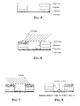
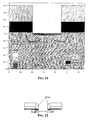
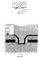
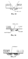
- the photolithographic step for defining the Schottky contact area inside the aperture of a discrete or of an elementary cell of an integrated structure of the insulated gate power device is eliminated by carrying out:
- the invention provides a method for integrating a Schottky contact inside the apertures of the elementary cells that constitute the integrated structure of the insulated gate power device in a totally self-alignment manner without requiring a dedicated masking step.
- the process of this invention differs from the known processes for the realization of a structure of an insulated gate device with Schottky diode integrated in the elementary cells that compose the device, because of the way in which the elementary cell structure is realized such to include a Schottky contact between the source metal layer and a region of semiconductor crystal of substrate electrically coinciding with the drain of the integrated power device.
- process steps that characterize the invention may be introduced in any process flow for the fabrication of an integrated floating gate power device, such as a power MOS or briefly PMOS. For this reason, specific dimensional details of structural features and relative doses and implantation energies of the dopants are not indicated, given that these may vary from a process to another depending on fabrication technology, particular needs and/or preferences of the manufacturer.
- an implantation (which hereinafter will be referred to as of "drain engineering" or D.E.) is included in the process sequence for increasing the resistivity of the semiconductor of substrate (drain) of the device under the Schottky contact region.
- the semiconductor substrate of drain may be in practice an epitomical layer grown on a semiconductor crystal that may have electrical characteristics different from those of the epitaxial layer grown thereon.
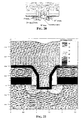
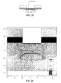
- An implanted buried region of "drain engineering" will be electrically tied to the body or, where they exists, to the deep body diffusions, such to effectively shield the Schottky contact also in a vertical direction, with the result of decisively reducing the leakage current.
- the realized integrated structure may be defined as "Lateral & Vertical Merged PiN Schottky (LVMPS)".
- the invention has been illustrated for the case of fabrication of a N channel PMOS, the invention can be practiced also for fabricating a P channel PMOS, by inverting the types of dopants.
- stripe layout is not mandatory, other cellular layouts may be used, eventually performing several pairs of body implantations each with appropriate tilts and twist angles in order to realize the body diffusions in each channel zone while defining a Shottky contact window there between.
- a self-aligned Schottky contact in a "window" defined by the use of angled implantations in the middle of the cell area may be extended even to a structure with traditional contacts (that is defined and opened by photolithography).
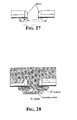
- the etching of silicon for forming the microtrench will not be self-aligned to the window opened by photolithography through the polysilicon, but self-aligned to the contact openings.
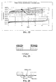
- the graph of Figure 30 shows the leakage current and the direct voltage drop obtained on test structures for different doses of drain engineering dopant. Near the dose of 2* 10 12 ions/cm 2 there is enough room for reducing the leakage by an order of magnitude without burdening excessively the direct voltage drop. By doubling the dose, the drain engineering diffusion creates a junction that shields the Schottky contact but reduces the direct characteristic to become practically similar to that of a PN junction diode.
Landscapes
- Electrodes Of Semiconductors (AREA)
- Insulated Gate Type Field-Effect Transistor (AREA)
Claims (4)
- Procédé pour fabriquer un dispositif de puissance intégré à grille isolée, comprenant les étapes suivantes :a) constituer un substrat semiconducteur de drain dopé avec un dopant d'un premier type de conductivité et former une structure de bord du dispositif de puissance intégré à grille isolée,b) former une électrode de grille isolée par croissance ou par dépôt d'un film diélectrique d'oxyde de grille sur la surface du substrat semiconducteur de drain et déposer dessus une couche conductrice de silicium polycristallin,c) recouvrir la couche conductrice de silicium polycristallin d'une couche ou d'une multicouche isolante d'un matériau diélectrique déposé dessus,d) déposer une couche de résine photosensible sur la couche isolante déposée,e) définir l'électrode de grille en masquant et en gravant de façon sélective et anisotrope la couche isolante déposée et la couche de silicium polycristallin, formant des ouvertures dans la zone où vont être formés la structure intégrée et le contact de source associé de chaque cellule élémentaire constituant ledit dispositif de puissance,
et caractérisé par les étapes successives suivantef) réaliser une première implantation d'ions d'un dopant approprié pour constituer une région de corps du type de conductivité opposé à celui du substrat semiconducteur de drain avec certains angles d'inclinaison et de torsion de façon à déterminer une zone d'ombre non implantée à l'intérieur de ladite ouverture en fonction de la hauteur totale du bord de définition de l'empilement composé de la couche de silicium polycristallin, de la couche isolante et de la couche de résine photosensible, et de la largeur de l'ouverture, avec une dose d'implants et une énergie appropriée pour obtenir une certaine concentration et une certaine longueur de canal ;g) réaliser au moins une deuxième implantation d'ions dans les mêmes conditions que la première implantation mais avec des angles d'inclinaison et de torsion différents pour définir une fenêtre centrale non implantée dans le motif d'ombre sur la zone de la cellule implantée ;h) retirer la couche de résine photosensible ;i) activer les dopants implantés par un traitement thermique ;j) réaliser une implantation d'ions de source sur la totalité de la surface de ladite ouverture à l'aide d'un dopant du même type de conductivité que celui du substrat de drain et opposé à celui du dopant des implantations de corps avec une dose et une énergie d'implantation appropriées pour constituer une région de source entourée par la région de corps ;k) activer les dopants de source implantés par un traitement thermique ;l) déposer une couche sacrificielle d'un matériau diélectrique dans des conditions sensiblement uniformes d'épaisseur de dépôt sur les gradins des frontières de définition desdites ouvertures ;m) graver de façon anisotrope la couche sacrificielle pour laisser un espaceur diélectrique sur les surfaces de bord de définition desdites ouvertures ;n) graver de façon anisotrope le semiconducteur sur une profondeur supérieure à la profondeur de la région de source mais inférieure à la profondeur de la région de corps, exposant dans la zone de chaque surface de cellule de la région de source, de la région de corps et, au fond de la tranchée, une zone du substrat de drain entourée latéralement par la région de corps ;o) ouvrir des contacts sur l'électrode de grille à travers un masque de résine photosensible dédié ;p) retirer le masque de résine photosensible et déposer une ou plusieurs couches métalliques conductrices pour établir à l'intérieur de ladite tranchée un contact électrique avec à la fois la région de source et la région de corps et déterminer une hauteur de barrière du contact Schottky établi avec le substrat de drain sur au moins une partie de la surface du fond de ladite tranchée. - Procédé de fabrication d'un dispositif de puissance intégré à grille isolée, comprenant les étapes suivantes :a) constituer un substrat semiconducteur de drain dopé avec un dopant d'un premier type de conductivité et former une structure de bord du dispositif de puissance intégré à grille isolée,b) former une électrode de grille isolée par croissance ou par dépôt d'un film diélectrique d'oxyde de grille sur la surface du substrat semiconducteur de drain et déposer dessus une couche conductrice de silicium polycristallin,c) recouvrir la couche conductrice de silicium polycristallin d'une couche ou d'une multicouche isolante d'un matériau diélectrique déposé dessus,d) déposer une couche de résine photosensible sur la couche isolante déposée,e) définir l'électrode de grille en masquant et en gravant de façon sélective et anisotrope la couche isolante déposée et la couche de silicium polycristallin, formant des ouvertures dans la zone où vont être formés la structure intégrée et le contact de source associé de chaque cellule élémentaire constituant ledit dispositif de puissance,
et caractérisé par les étapes successives suivantef) réaliser une première implantation d'ions d'un dopant approprié pour constituer une région de corps profond du type de conductivité opposé à celui du substrat semiconducteur de drain avec certains angles d'inclinaison et de torsion de façon à déterminer une zone d'ombre non implantée à l'intérieur de ladite ouverture en fonction de la hauteur totale du bord de définition de l'empilement composé de la couche de silicium polycristallin, de la couche isolante et de la couche de résine photosensible, et de la largeur de l'ouverture, avec une dose d'implants et une énergie appropriée pour obtenir une certaine concentration et une certaine profondeur d'implants ;g) réaliser au moins une deuxième implantation d'ions dans les mêmes conditions que la première implantation mais avec des angles d'inclinaison et de torsion différents pour définir une fenêtre centrale non implantée dans le motif d'ombre sur la zone de la cellule implantée ;h) retirer la couche de résine photosensible ;i) réaliser au moins une troisième implantation d'ions d'un dopant approprié pour constituer une région de corps du type de conductivité opposé à celui du substrat semiconducteur de drain avec certains angles d'inclinaison et de torsion, de façon à déterminer une zone d'ombre non implantée à l'intérieur de ladite ouverture en fonction de la hauteur totale du bord de définition de l'empilement composé de la couche de silicium polycristallin et de la couche isolante, et de la largeur de l'ouverture, avec une dose d'implants et une énergie appropriée pour obtenir une certaine concentration et une certaine longueur de canal ;j) réaliser au moins une quatrième implantation d'ions dans les mêmes conditions que la troisième implantation d'ions mais avec des angles d'inclinaison et de torsion différents pour définir une fenêtre centrale non implantée dans le motif d'ombre de la zone de cellule implantée ;k) activer les dopants implantés de corps et de corps profond par un traitement thermique ;l) réaliser une implantation d'ions de source sur la totalité de la surface de ladite ouverture à l'aide d'un dopant du même type de conductivité que celui du substrat de drain et opposé à celui des dopants des implantations de corps et de corps profond, avec une dose et une énergie d'implantation appropriée pour constituer une région de source entourée par la région de corps ;m) activer les dopants de source implantés par un traitement thermique ;n) déposer une couche sacrificielle de matériau diélectrique dans des conditions sensiblement uniformes d'épaisseur de dépôt sur les gradins des frontières de définition desdites ouvertures ;o) graver de façon anisotrope la couche sacrificielle pour laisser un espaceur diélectrique sur les surfaces de bord de définition desdites ouvertures ;p) graver de façon anisotrope le semiconducteur sur une profondeur supérieure à la profondeur de la région de source mais inférieure à la profondeur de la région de corps, exposant dans la zone de chaque surface de cellule de la région de source, de la région de corps, et, au fond de la tranchée, ladite région de corps profond et une zone du substrat de drain entourée latéralement par la région de corps profond ;q) ouvrir des contacts sur l'électrode de grille à travers un masque de résine photosensible dédié ;r) retirer le masque de résine photosensible et déposer une ou plusieurs couches métalliques conductrices pour établir à l'intérieur de ladite tranchée un contact électrique avec à la fois la région de source et la région de corps et déterminer une hauteur de barrière du contact Schottky établi avec le substrat de drain sur au moins une partie de la surface du fond de la tranchée. - Procédé de fabrication d'un dispositif selon la revendication 1 ou 2, caractérisé en ce qu'il comprend une étape ultérieure consistant à réaliser, après avoir défini l'électrode de grille avec la formation desdites ouvertures, une implantation d'ions avec une énergie suffisamment élevée pour implanter un dopant du même type conductivité que le dopant utilisé pour réaliser la région de corps dans une région enterrée à une profondeur supérieure à celle du fond des régions de corps, avec une dose telle qu'elle surcompense ou sous-compense légèrement la concentration de dopants du type de conductivité opposé à celui du substrat de drain pour créer une région de blindage sous le contact Schottky.
- Procédé de fabrication d'un dispositif selon la revendication 3, caractérisé en ce que la dose de dopants implantés n'est pas suffisante pour compenser complètement la concentration en dopants du type de conductivité opposé à celui du substrat de drain.
Priority Applications (4)
| Application Number | Priority Date | Filing Date | Title |
|---|---|---|---|
| EP10180038.1A EP2259327B1 (fr) | 2002-11-14 | 2002-11-14 | Dispositif semi-conducteur de puissance à grille isolée et diode Schottky et procédé de fabrication correspondant |
| EP02425695A EP1420457B1 (fr) | 2002-11-14 | 2002-11-14 | Procédé de fabrication d'un dispositif semi-conducteur de puissance à grille isolée et diode Schottky |
| US10/713,778 US20040164304A1 (en) | 2002-11-14 | 2003-11-14 | Insulated gate planar integrated power device with co-integrated schottky diode and process |
| US11/520,210 US7560368B2 (en) | 2002-11-14 | 2006-09-12 | Insulated gate planar integrated power device with co-integrated Schottky diode and process |
Applications Claiming Priority (1)
| Application Number | Priority Date | Filing Date | Title |
|---|---|---|---|
| EP02425695A EP1420457B1 (fr) | 2002-11-14 | 2002-11-14 | Procédé de fabrication d'un dispositif semi-conducteur de puissance à grille isolée et diode Schottky |
Related Child Applications (2)
| Application Number | Title | Priority Date | Filing Date |
|---|---|---|---|
| EP10180038.1A Division EP2259327B1 (fr) | 2002-11-14 | 2002-11-14 | Dispositif semi-conducteur de puissance à grille isolée et diode Schottky et procédé de fabrication correspondant |
| EP10180038.1 Division-Into | 2010-09-27 |
Publications (2)
| Publication Number | Publication Date |
|---|---|
| EP1420457A1 EP1420457A1 (fr) | 2004-05-19 |
| EP1420457B1 true EP1420457B1 (fr) | 2012-01-11 |
Family
ID=32116366
Family Applications (2)
| Application Number | Title | Priority Date | Filing Date |
|---|---|---|---|
| EP10180038.1A Expired - Lifetime EP2259327B1 (fr) | 2002-11-14 | 2002-11-14 | Dispositif semi-conducteur de puissance à grille isolée et diode Schottky et procédé de fabrication correspondant |
| EP02425695A Expired - Lifetime EP1420457B1 (fr) | 2002-11-14 | 2002-11-14 | Procédé de fabrication d'un dispositif semi-conducteur de puissance à grille isolée et diode Schottky |
Family Applications Before (1)
| Application Number | Title | Priority Date | Filing Date |
|---|---|---|---|
| EP10180038.1A Expired - Lifetime EP2259327B1 (fr) | 2002-11-14 | 2002-11-14 | Dispositif semi-conducteur de puissance à grille isolée et diode Schottky et procédé de fabrication correspondant |
Country Status (2)
| Country | Link |
|---|---|
| US (2) | US20040164304A1 (fr) |
| EP (2) | EP2259327B1 (fr) |
Families Citing this family (40)
| Publication number | Priority date | Publication date | Assignee | Title |
|---|---|---|---|---|
| US7294882B2 (en) * | 2004-09-28 | 2007-11-13 | Sandisk Corporation | Non-volatile memory with asymmetrical doping profile |
| DE102004057235B4 (de) * | 2004-11-26 | 2007-12-27 | Infineon Technologies Ag | Vertikaler Trenchtransistor und Verfahren zu dessen Herstellung |
| EP1742271A1 (fr) * | 2005-07-08 | 2007-01-10 | STMicroelectronics S.r.l. | Transistor de puissance à effet de champ et procédé de fabrication correspondant |
| US8080848B2 (en) | 2006-05-11 | 2011-12-20 | Fairchild Semiconductor Corporation | High voltage semiconductor device with lateral series capacitive structure |
| US7618867B2 (en) * | 2006-07-26 | 2009-11-17 | Infineon Technologies Ag | Method of forming a doped portion of a semiconductor and method of forming a transistor |
| US20080296636A1 (en) * | 2007-05-31 | 2008-12-04 | Darwish Mohamed N | Devices and integrated circuits including lateral floating capacitively coupled structures |
| US7807555B2 (en) * | 2007-07-31 | 2010-10-05 | Intersil Americas, Inc. | Method of forming the NDMOS device body with the reduced number of masks |
| JP2009218580A (ja) * | 2008-03-06 | 2009-09-24 | Toshiba Corp | 2方向ハロ注入 |
| US8193565B2 (en) | 2008-04-18 | 2012-06-05 | Fairchild Semiconductor Corporation | Multi-level lateral floating coupled capacitor transistor structures |
| WO2011033550A1 (fr) | 2009-09-15 | 2011-03-24 | 株式会社 東芝 | Dispositif à semi-conducteurs |
| US8368140B2 (en) * | 2009-12-03 | 2013-02-05 | Diodes Incorporated | Trench MOS device with Schottky diode and method for manufacturing same |
| US8624302B2 (en) * | 2010-02-05 | 2014-01-07 | Fairchild Semiconductor Corporation | Structure and method for post oxidation silicon trench bottom shaping |
| TWI425575B (zh) * | 2010-07-09 | 2014-02-01 | 陳自雄 | 低閘容金氧半p-n接面二極體結構及其製作方法 |
| DE102010051874A1 (de) | 2010-11-22 | 2012-05-24 | Init Innovative Informatikanwendungen In Transport-, Verkehrs- Und Leitsystemen Gmbh | Schaltung zum Schutz gegen Verpolung |
| EP2500848A1 (fr) | 2011-03-15 | 2012-09-19 | Amadeus S.A.S. | Procédé et système pour la gestion centralisée de contexte de réservation dans un système de réservation de serveurs multiples |
| US8716825B2 (en) * | 2011-06-22 | 2014-05-06 | Macronix International Co., Ltd. | Semiconductor structure and manufacturing method for the same |
| CN102842596B (zh) * | 2011-06-22 | 2015-05-20 | 旺宏电子股份有限公司 | 半导体结构及其制造方法 |
| US8736013B2 (en) | 2012-04-19 | 2014-05-27 | Fairchild Semiconductor Corporation | Schottky diode with opposite-polarity schottky diode field guard ring |
| US20130313570A1 (en) * | 2012-05-24 | 2013-11-28 | Microsemi Corporation | Monolithically integrated sic mosfet and schottky barrier diode |
| US9018048B2 (en) | 2012-09-27 | 2015-04-28 | Stmicroelectronics S.R.L. | Process for manufactuirng super-barrier rectifiers |
| EP2911205B1 (fr) | 2012-10-19 | 2020-12-09 | Nissan Motor Co., Ltd | Dispositif semi-conducteur et son procédé de fabrication |
| WO2014168430A1 (fr) * | 2013-04-10 | 2014-10-16 | 주식회사 실리콘웍스 | Procédé de fabrication de circuit redresseur |
| CN104518006B (zh) * | 2014-07-01 | 2017-03-15 | 重庆中科渝芯电子有限公司 | 一种耗尽型沟道超势垒整流器及其制造方法 |
| WO2016179025A1 (fr) | 2015-05-01 | 2016-11-10 | The Regents Of The University Of California | Réalisation de modèles de couche de circuit intégré par implantation d'ions inclinée |
| CN106257626B (zh) * | 2015-06-19 | 2019-05-14 | 北大方正集团有限公司 | 肖特基器件制作方法及肖特基器件 |
| US10096681B2 (en) | 2016-05-23 | 2018-10-09 | General Electric Company | Electric field shielding in silicon carbide metal-oxide-semiconductor (MOS) device cells |
| DE102016111940B4 (de) * | 2016-06-29 | 2019-07-25 | Infineon Technologies Austria Ag | Verfahren zum Herstellen einer Superjunction-Halbleitervorrichtung und Superjunction-Halbleitervorrichtung |
| CN106098752A (zh) * | 2016-07-25 | 2016-11-09 | 吉林华微电子股份有限公司 | 一种igbt器件及其制造方法 |
| US9941171B1 (en) * | 2016-11-18 | 2018-04-10 | Monolithic Power Systems, Inc. | Method for fabricating LDMOS with reduced source region |
| CN107154346B (zh) * | 2017-05-19 | 2021-03-16 | 京东方科技集团股份有限公司 | 一种膜层的掺杂方法、薄膜晶体管及其制作方法 |
| CN108899364B (zh) * | 2018-07-02 | 2020-06-16 | 电子科技大学 | 一种集成肖特基二极管的mos栅控晶闸管及其制备方法 |
| CN110212026B (zh) * | 2019-05-06 | 2022-09-16 | 上海功成半导体科技有限公司 | 超结mos器件结构及其制备方法 |
| EP3742476B1 (fr) * | 2019-05-20 | 2024-11-06 | Infineon Technologies AG | Procédé d'implantation d'une espèce d'implant dans un substrat à différentes profondeurs |
| WO2020252306A1 (fr) * | 2019-06-14 | 2020-12-17 | Silcotek Corp. | Croissance de nanofils |
| CN112864222B (zh) * | 2019-11-27 | 2022-04-12 | 苏州东微半导体股份有限公司 | 半导体功率器件 |
| CN112864150B (zh) * | 2019-11-27 | 2022-04-15 | 苏州东微半导体股份有限公司 | 超结功率器件 |
| TW202137333A (zh) * | 2020-03-24 | 2021-10-01 | 立錡科技股份有限公司 | 具有橫向絕緣閘極雙極性電晶體之功率元件及其製造方法 |
| CN112002751A (zh) * | 2020-07-22 | 2020-11-27 | 湖南国芯半导体科技有限公司 | 碳化硅vdmosfet器件的元胞结构、其制备方法及碳化硅vdmosfet器件 |
| TWI773029B (zh) | 2020-12-17 | 2022-08-01 | 國立清華大學 | 具有溝槽式接面蕭基位障二極體的半導體結構 |
| CN115527860B (zh) * | 2022-11-04 | 2023-04-07 | 合肥晶合集成电路股份有限公司 | 半导体结构的制作方法以及半导体结构 |
Citations (2)
| Publication number | Priority date | Publication date | Assignee | Title |
|---|---|---|---|---|
| JPH03105979A (ja) * | 1989-09-20 | 1991-05-02 | Hitachi Ltd | 絶縁ゲート半導体装置およびその製造方法 |
| DE10005774A1 (de) * | 2000-02-10 | 2001-08-23 | Infineon Technologies Ag | DMOS-Zelle mit Schottky-Diode |
Family Cites Families (7)
| Publication number | Priority date | Publication date | Assignee | Title |
|---|---|---|---|---|
| US5528058A (en) * | 1986-03-21 | 1996-06-18 | Advanced Power Technology, Inc. | IGBT device with platinum lifetime control and reduced gaw |
| JPH0693512B2 (ja) | 1986-06-17 | 1994-11-16 | 日産自動車株式会社 | 縦形mosfet |
| JP2573736B2 (ja) * | 1990-09-18 | 1997-01-22 | 三菱電機株式会社 | 高耐圧低抵抗半導体装置及びその製造方法 |
| EP0696054B1 (fr) * | 1994-07-04 | 2002-02-20 | STMicroelectronics S.r.l. | Procédé de manufacture des dispositifs de puissance à haute densité en technology MOS |
| US5886383A (en) | 1997-01-10 | 1999-03-23 | International Rectifier Corporation | Integrated schottky diode and mosgated device |
| US6140214A (en) * | 1998-08-28 | 2000-10-31 | Micron Technology, Inc. | Semiconductor processing methods, semiconductor processing methods of forming diodes, and semiconductor processing methods of forming schottky diodes |
| US6724039B1 (en) * | 1998-08-31 | 2004-04-20 | Stmicroelectronics, Inc. | Semiconductor device having a Schottky diode |
-
2002
- 2002-11-14 EP EP10180038.1A patent/EP2259327B1/fr not_active Expired - Lifetime
- 2002-11-14 EP EP02425695A patent/EP1420457B1/fr not_active Expired - Lifetime
-
2003
- 2003-11-14 US US10/713,778 patent/US20040164304A1/en not_active Abandoned
-
2006
- 2006-09-12 US US11/520,210 patent/US7560368B2/en not_active Expired - Lifetime
Patent Citations (2)
| Publication number | Priority date | Publication date | Assignee | Title |
|---|---|---|---|---|
| JPH03105979A (ja) * | 1989-09-20 | 1991-05-02 | Hitachi Ltd | 絶縁ゲート半導体装置およびその製造方法 |
| DE10005774A1 (de) * | 2000-02-10 | 2001-08-23 | Infineon Technologies Ag | DMOS-Zelle mit Schottky-Diode |
Also Published As
| Publication number | Publication date |
|---|---|
| EP2259327B1 (fr) | 2014-04-02 |
| EP1420457A1 (fr) | 2004-05-19 |
| EP2259327A3 (fr) | 2011-06-29 |
| EP2259327A2 (fr) | 2010-12-08 |
| US7560368B2 (en) | 2009-07-14 |
| US20070102725A1 (en) | 2007-05-10 |
| US20040164304A1 (en) | 2004-08-26 |
Similar Documents
| Publication | Publication Date | Title |
|---|---|---|
| EP1420457B1 (fr) | Procédé de fabrication d'un dispositif semi-conducteur de puissance à grille isolée et diode Schottky | |
| US7696571B2 (en) | Method of manufacturing a trench transistor having a heavy body region | |
| US7084034B2 (en) | High voltage MOS-gated power device and related manufacturing process | |
| US5656843A (en) | Semiconductor device having a vertical insulated gate field effect device and a breakdown region remote from the gate | |
| US7041560B2 (en) | Method of manufacturing a superjunction device with conventional terminations | |
| US5342797A (en) | Method for forming a vertical power MOSFET having doped oxide side wall spacers | |
| US6624030B2 (en) | Method of fabricating power rectifier device having a laterally graded P-N junction for a channel region | |
| US7161208B2 (en) | Trench mosfet with field relief feature | |
| US20170098609A1 (en) | Source-Gate Region Architecture in a Vertical Power Semiconductor Device | |
| US6107127A (en) | Method of making shallow well MOSFET structure | |
| HK1109495B (en) | Field effect transistor and method of its manufacture |
Legal Events
| Date | Code | Title | Description |
|---|---|---|---|
| PUAI | Public reference made under article 153(3) epc to a published international application that has entered the european phase |
Free format text: ORIGINAL CODE: 0009012 |
|
| AK | Designated contracting states |
Kind code of ref document: A1 Designated state(s): AT BE BG CH CY CZ DE DK EE ES FI FR GB GR IE IT LI LU MC NL PT SE SK TR |
|
| AX | Request for extension of the european patent |
Extension state: AL LT LV MK RO SI |
|
| 17P | Request for examination filed |
Effective date: 20041115 |
|
| AKX | Designation fees paid |
Designated state(s): DE FR GB IT |
|
| 17Q | First examination report despatched |
Effective date: 20081103 |
|
| RAP1 | Party data changed (applicant data changed or rights of an application transferred) |
Owner name: STMICROELECTRONICS SRL |
|
| GRAP | Despatch of communication of intention to grant a patent |
Free format text: ORIGINAL CODE: EPIDOSNIGR1 |
|
| RTI1 | Title (correction) |
Free format text: MANUFACTURING METHOD OF AN INSULATED GATE POWER SEMICONDUCTOR DEVICE WITH SCHOTTKY DIODE |
|
| GRAS | Grant fee paid |
Free format text: ORIGINAL CODE: EPIDOSNIGR3 |
|
| GRAA | (expected) grant |
Free format text: ORIGINAL CODE: 0009210 |
|
| AK | Designated contracting states |
Kind code of ref document: B1 Designated state(s): DE FR GB IT |
|
| REG | Reference to a national code |
Ref country code: GB Ref legal event code: FG4D |
|
| REG | Reference to a national code |
Ref country code: DE Ref legal event code: R096 Ref document number: 60241946 Country of ref document: DE Effective date: 20120308 |
|
| RAP2 | Party data changed (patent owner data changed or rights of a patent transferred) |
Owner name: STMICROELECTRONICS SRL |
|
| PLBE | No opposition filed within time limit |
Free format text: ORIGINAL CODE: 0009261 |
|
| STAA | Information on the status of an ep patent application or granted ep patent |
Free format text: STATUS: NO OPPOSITION FILED WITHIN TIME LIMIT |
|
| PG25 | Lapsed in a contracting state [announced via postgrant information from national office to epo] |
Ref country code: IT Free format text: LAPSE BECAUSE OF FAILURE TO SUBMIT A TRANSLATION OF THE DESCRIPTION OR TO PAY THE FEE WITHIN THE PRESCRIBED TIME-LIMIT Effective date: 20120111 |
|
| 26N | No opposition filed |
Effective date: 20121012 |
|
| REG | Reference to a national code |
Ref country code: DE Ref legal event code: R097 Ref document number: 60241946 Country of ref document: DE Effective date: 20121012 |
|
| GBPC | Gb: european patent ceased through non-payment of renewal fee |
Effective date: 20121114 |
|
| PG25 | Lapsed in a contracting state [announced via postgrant information from national office to epo] |
Ref country code: GB Free format text: LAPSE BECAUSE OF NON-PAYMENT OF DUE FEES Effective date: 20121114 |
|
| PGFP | Annual fee paid to national office [announced via postgrant information from national office to epo] |
Ref country code: FR Payment date: 20131121 Year of fee payment: 12 |
|
| REG | Reference to a national code |
Ref country code: DE Ref legal event code: R082 Ref document number: 60241946 Country of ref document: DE |
|
| REG | Reference to a national code |
Ref country code: FR Ref legal event code: ST Effective date: 20150731 |
|
| PG25 | Lapsed in a contracting state [announced via postgrant information from national office to epo] |
Ref country code: FR Free format text: LAPSE BECAUSE OF NON-PAYMENT OF DUE FEES Effective date: 20141201 |
|
| PGFP | Annual fee paid to national office [announced via postgrant information from national office to epo] |
Ref country code: DE Payment date: 20211020 Year of fee payment: 20 |
|
| REG | Reference to a national code |
Ref country code: DE Ref legal event code: R071 Ref document number: 60241946 Country of ref document: DE |