EP1422845A2 - Verfahren und Vorrichtung zur optischen Dispersionsüberwachung - Google Patents
Verfahren und Vorrichtung zur optischen Dispersionsüberwachung Download PDFInfo
- Publication number
- EP1422845A2 EP1422845A2 EP03026699A EP03026699A EP1422845A2 EP 1422845 A2 EP1422845 A2 EP 1422845A2 EP 03026699 A EP03026699 A EP 03026699A EP 03026699 A EP03026699 A EP 03026699A EP 1422845 A2 EP1422845 A2 EP 1422845A2
- Authority
- EP
- European Patent Office
- Prior art keywords
- signal
- dispersion
- optical
- monitoring apparatus
- comparator
- Prior art date
- Legal status (The legal status is an assumption and is not a legal conclusion. Google has not performed a legal analysis and makes no representation as to the accuracy of the status listed.)
- Granted
Links
Images


Classifications
-
- H—ELECTRICITY
- H04—ELECTRIC COMMUNICATION TECHNIQUE
- H04B—TRANSMISSION
- H04B10/00—Transmission systems employing electromagnetic waves other than radio-waves, e.g. infrared, visible or ultraviolet light, or employing corpuscular radiation, e.g. quantum communication
- H04B10/25—Arrangements specific to fibre transmission
- H04B10/2507—Arrangements specific to fibre transmission for the reduction or elimination of distortion or dispersion
- H04B10/2513—Arrangements specific to fibre transmission for the reduction or elimination of distortion or dispersion due to chromatic dispersion
Definitions
- the present invention relates to a technique for monitoring optical dispersion based on waveforms of transmitted light.
- the present invention relates to an optical dispersion monitoring apparatus and an optical dispersion monitoring method, capable of monitoring dispersion accurately with a simple construction, and to an optical transmission system using the same.
- an optical signal sent to a transmission path 101 by an optical transmission apparatus 100 is transmitted for several tens of kilometers to several thousands of kilometers through an optical fiber via optical repeaters 102 using optical amplifiers or signal regenerators, to be received by an optical receiving apparatus 103.
- waveform distortion occurs in the optical signal being transmitted, due to nonlinear optical phenomena occurring in the optical fiber depending on a dispersion characteristic of the optical fiber or the intensity of the optical signal, a change in instantaneous optical frequency of a pulse added in the optical transmission apparatus 100, and the like.
- FIG. 17 shows an example in which a variable dispersion compensator 104A and a fixed variable compensator 104B are connected in series to construct a dispersion compensator 104.
- an optical dispersion monitoring apparatus 105 is required for determining whether a compensation amount is optimal or not, while the system is operating.
- a structure in which cumulative dispersion is detected by paying attention to the spectral shape or spectral intensity at a specific frequency of a received optical signal Furthermore, there is also known a structure in which the error rate of a regenerated signal at a required monitoring location is measured to detect cumulative dispersion.
- the present invention has been accomplished in view of the above described problems, with an object of providing an apparatus and a method for monitoring optical dispersion, capable of monitoring dispersion accurately with a simple construction, and an optical transmission system using the same.
- an optical dispersion monitoring apparatus of the present invention for monitoring dispersion based on a waveform of an input optical signal, comprises: a characteristic amount detecting section selectively detecting a physical amount corresponding to a location where waveform distortion occurring depending on dispersion appears distinctively in the waveform of the input optical signal; and a dispersion information extracting section extracting information related to the dispersion occurred in the optical signal, based on a comparison between the physical amount detected in the characteristic amount detecting section and a reference value indicated by a reference signal, to output the information.
- an input optical signal is supplied to the characteristic amount detecting section, the physical amount corresponding to the location where the waveform distortion occurring depending on dispersion appears distinctively in the signal waveform is detected selectively, and the detection result is transmitted to the dispersion information extracting section.
- the dispersion information extracting section the physical amount detected in the characteristic amount detecting section is compared with the reference value indicated in the reference signal, and information related to the dispersion occurred in the optical signal is extracted based on the comparison result.
- the construction may be such that the characteristic amount detecting section includes: a light receiving section converting the input optical signal into an electrical signal; and a signal transition position detecting section detecting the voltage level corresponding to at least one of a rising edge and a falling edge of waveform of the electrical signal converted in the light receiving section, and the dispersion information extracting section compares the reference value indicated by the reference signal with the voltage level detected in the signal transition position detecting section, and outputs a signal corresponding to the comparison result as dispersion information.
- the characteristic amount detecting section includes: a light receiving section converting the input optical signal into an electrical signal; and a signal transition position detecting section detecting the voltage level corresponding to at least one of a rising edge and a falling edge of waveform of the electrical signal converted in the light receiving section, and the dispersion information extracting section compares the reference value indicated by the reference signal with the voltage level detected in the signal transition position detecting section, and outputs a signal corresponding to the comparison result as dispersion information.
- the voltage level corresponding to the rising edge or the falling edge of the waveform of the electrical signal converted in the light receiving section is detected as the physical amount corresponding to the location where the waveform distortion appears distinctively, and the dispersion information is extracted based on the comparison of the voltage level and the reference value.
- the construction may be such that the characteristic amount detecting section includes: a light receiving section converting the input optical signal into an electrical signal; and a signal intensity detecting section detecting the average intensity of waveform of the electrical signal converted in the light receiving section, by sampling parts of the waveform at the center of one cycle and locations neighboring the center in accordance with a clock signal synchronized with the input optical signal, and the dispersion information extracting section compares the average intensity detected in the signal intensity detecting section with the reference value indicated by the reference signal, and outputs a signal corresponding to the comparison result as dispersion information.
- the characteristic amount detecting section includes: a light receiving section converting the input optical signal into an electrical signal; and a signal intensity detecting section detecting the average intensity of waveform of the electrical signal converted in the light receiving section, by sampling parts of the waveform at the center of one cycle and locations neighboring the center in accordance with a clock signal synchronized with the input optical signal, and the dispersion information extracting section compares the average intensity detected in the signal intensity detecting section
- the average intensity of waveform of the electrical signal converted in the light receiving section, at the center of one cycle and the locations neighboring the center, is detected as a physical amount corresponding to the location where the waveform distortion appears distinctively, and dispersion information is extracted based on the comparison of the average intensity and the reference value.
- an optical dispersion monitoring method of the present invention for monitoring dispersion based on a waveform of an input optical signal, comprises: selectively detecting a physical amount corresponding to a location where waveform distortion occurring depending on dispersion appears distinctively in the waveform of the input optical signal; and extracting information related to the dispersion occurred in the optical signal, based on a comparison between the detected physical amount detected and a reference value indicated by a reference signal.
- an optical transmission system of the present invention provided with a variable dispersion compensator on a transmission path through which an optical signal is propagated, for controlling a compensation amount of the variable dispersion compensator to dynamically compensate for dispersion, is constructed so that using the optical dispersion monitoring apparatus of the present invention, dispersion occurred in the optical signal being propagated through the transmission path is monitored and the compensation amount of the variable dispersion compensator is controlled in accordance with the monitored result.
- the variable dispersion compensator is controlled using the optical dispersion monitoring apparatus of the present invention, it is possible to perform dynamic compensation for dispersion occurred in the optical transmission system easily and reliably.
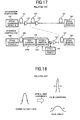
- FIG. 1 is a block diagram showing a structure of an optical dispersion monitoring apparatus according to a first embodiment of the present invention.
- FIG. 2 is a block diagram showing an example of a main structure of an optical transmission system in which dynamic dispersion compensation is performed using the optical dispersion monitoring apparatus of FIG. 1.
- an optical dispersion monitoring apparatus 1 of the present embodiment is provided with, for example, a light receiving section 10 converting an optical signal input thereto into an electrical signal to output it, a signal transition position detecting section 20 detecting the voltage level corresponding to at least one of the rising edge and falling edge of an input light waveform based on the output signal from the light receiving section 10, and a cumulative dispersion information extracting section 30 extracting information related to cumulative dispersion occurred in the input light, based on the detection result in the signal transition position detecting section 20.
- the light receiving section 10 converts, for example, an optical signal input to the optical dispersion monitoring apparatus 1 into a current signal using a known light receiving element, and converts the current signal into a voltage signal V IN , to output it to the signal transition position detecting section 20.
- the voltage signal V IN output from this light receiving section 10 is a signal whose level is changed depending on the power of the input light.
- the optical signal input to the optical dispersion monitoring apparatus 1 is an optical signal that has a crossing point in an eye pattern drawn by folding back a time waveform of the optical signal in one cycle, that is, an optical signal applied with a code type in which the signal level has no transition during one bit cycle.
- a representative example of such an optical signal is an optical signal of NRZ type.
- optical signals capable of being input to the optical dispersion monitoring apparatus 1 are not limited to NRZ type.
- the signal transition position detecting section 20 includes a comparator 21, a slice amplifier 22 and a low-pass filter 23.
- the comparator 21 receives a voltage signal V IN output from the light receiving section 10 at one input terminal thereof and a feedback signal V X transmitted through the low-pass filter 23 at the other input terminal, and compares the level of the voltage signal V IN with the level of the feedback signal V X , to output a voltage signal corresponding to the comparison result to the slice amplifier 22.
- a typical analog comparator may be used for this comparator 21.
- the slice amplifier 22 is a typical high gain amplifier which amplifies the voltage level of the output signal from the comparator 21 until it reaches the required high level or low level (here "1" or "0" level).
- the low-pass filter 23 smoothes the voltage signal amplified in the slice amplifier 22 in accordance with a preset time constant.
- the voltage signal V X which is transmitted through this low-pass filter 23 to be averaged, is fed back to the other input terminal of the comparator 21, and also sent to the cumulative dispersion information extracting section 30.
- the cumulative dispersion information extracting section 30 includes a comparator 31 and a reference signal generating circuit 32, as shown in FIG. 1 for example.
- the comparator 31 receives the voltage signal V X output from the signal transition position detecting section 20 at one input terminal thereof and a reference signal V REF generated in the reference signal generating circuit 32 at the other input terminal, and compares the level of the voltage signal V X with the level of the reference signal V REF , to output a voltage signal V OUT corresponding to the comparison result to outside the optical dispersion monitoring apparatus 1.
- Cumulative dispersion here means wavelength dispersion accumulated in an input light.
- the voltage signal V OUT output from the comparator 31 is supplied to a variable dispersion compensator 5 as shown in FIG.
- the reference signal generating circuit 32 applies, for example, an output voltage generated in a variable power source to the other input terminal of the comparator 31 as a reference signal V REF .
- This variable power source output voltage is set in advance depending on a mark ratio of an optical signal input to the optical dispersion monitoring apparatus 1, as described later.
- Reference numeral 4 in FIG. 2 denotes an optical amplifier for amplifying an optical signal for repeating transmission.
- reference numeral 6 denotes an optical coupler for branching a part of the optical signal output from the variable dispersion compensator 5 as a monitoring light and supplying it to the optical dispersion monitoring apparatus 1.
- the construction is such that the optical coupler 6 is disposed between the variable dispersion compensator 5 and the optical amplifier 4 to monitor cumulative dispersion.
- the position where the monitoring light is branched is not limited to the above.
- the constitutional example in which cumulative dispersion is compensated using only the variable dispersion compensator 5.
- an optical pulse is propagated through a transmission path using an optical fiber or the like, there is a difference in propagation speed between the rising edge and falling edge of the optical pulse depending on its optical wavelength and a dispersion characteristic of the optical fiber.
- the pulse is compressed, and conversely, in the case where the rising edge is advanced and the falling edge is delayed, the pulse is spread.
- the peak power is increased when the pulse is compressed, while the peak power being decreased when the pulse is spread.
- the optical dispersion monitoring apparatus 1 of the present embodiment enables cumulative dispersion, including up to positive or negative sign information, to be detected with a simple construction.
- the optical signal branched in the optical coupler 6 disposed on the transmission path 3 is sent to the light receiving section 10 to be converted into the voltage signal V IN , and supplied to the signal transition position detecting section 20.
- the waveform of the voltage signal V IN input to the signal transition position detecting section 20 distortion occurs depending on cumulative dispersion as shown in (A) of FIG. 4 for example.
- the waveform shown on the left side in (A) of FIG. 4 is one example of when the pulse is compressed
- the waveform on the right side is one example of when the pulse is spread.
- the comparator 21 compares the voltage signal V IN output from the light receiving section 10 with the voltage signal V X fed back through the low-pass filter 23, to output a voltage signal corresponding to the comparison result to the slice amplifier 22.
- the voltage signal V X from the low-pass filter 23 is set to the ground level or the like for example.
- the voltage signal output from the comparator 21 is amplified to the required level.
- the amplification operation in this slice amplifier 22 differs from an amplification operation in a linear amplifier as shown in a conceptual diagram of FIG. 5 for example, and the input signal thereto is amplified until it reaches the "1" or "0" level.
- the voltage signal amplified in the slice amplifier 22 is sent to the low-pass filter 23, smoothed (averaged) in accordance with a required time constant, and the voltage signal V X transmitted through the low-pass filter 23 is fed back to the comparator 21.
- the output signal of the comparator 21 is fed back to the comparator 21 via the slice amplifier 22 and the low-pass filter 23, so that the voltage level of the feedback signal becomes stable following the voltage level at the crossing points of the signal V IN input to the signal transition position detecting section 20 as shown in (B) of FIG. 4.
- the voltage signal V X fed back from the low-pass filter 23 to the comparator 21 a change in the rising edge or the falling edge of the input pulse over time is detected as a change in the voltage level at the crossing points.
- This voltage signal V X corresponding to the voltage level at the crossing points is sent to the cumulative dispersion information extracting section 30 as an output of the signal transition position detecting section 20.
- the comparator 31 compares the voltage signal V X output from the signal transition position detecting section 20 with the reference signal V REF output from the reference signal generating circuit 32, to output a voltage signal V OUT corresponding to the comparison result as cumulative dispersion information.
- the reference signal V REF supplied to the comparator 31 is set in advance with the fixed voltage level depending on the mark ratio of the optical signal input to the optical dispersion monitoring apparatus 1 as shown in (C) of FIG. 4.
- the fixed voltage level is set to approximately match the voltage level at the crossing points when the cumulative dispersion is 0.
- the fixed reference signal V REF set in this manner is supplied to the comparator 31, so that the voltage level of the voltage signal V OUT output from the comparator 31 corresponds to the cumulative dispersion as shown in (D) of FIG. 4.
- a negative value voltage signal V OUT is output as the cumulative dispersion information when the pulse is compressed, while a positive value voltage signal V OUT being output as the cumulative dispersion information when the pulse is spread.
- the relationship between the state of waveform distortion and the sign of the cumulative dispersion is that in the case where a chirp characteristic of a modulator on a transmission side of the optical transmission system is positive for example, the cumulative dispersion is negative when the pulse is compressed, while the cumulative dispersion being positive when the pulse is spread. Furthermore, in the case where the chirp characteristic is negative for example, the cumulative dispersion is positive when the pulse is compressed, while the cumulative dispersion being negative when the pulse is spread. Accordingly, in making the chirp characteristics of the system to correspond to the value of the above described voltage signal V OUT , it is possible to determine the cumulative dispersion including the sign information.
- the signal transition position detecting section 20 detects the voltage level at the crossing points of the optical signal to which a code type represented in NRZ type is applied, and the cumulative dispersion information extracting section 30 extracts the cumulative dispersion information based on the detection result.
- the present optical dispersion monitoring apparatus 1 does not require a signal regenerator as in the conventional system in which an error rate is measured. Hence, it is possible to reduce restrictions to the installation location in the optical transmission system. If the variable dispersion compensator 5 disposed in the optical transmission system is feedback controlled using such an optical dispersion monitoring apparatus 1, it is possible to perform easily and reliably dynamic compensation for cumulative dispersion occurring in the system.
- the wavelength dispersion accumulated in the input light has been considered as the cumulative dispersion.
- the present invention is not limited thereto.
- the present invention may be applied to other optical dispersion, such as polarization dispersion and the like, as in the case of the wavelength dispersion, if a relationship with the occurring state of waveform distortion can be specified.
- FIG. 6 is a block diagram showing a structure of the optical dispersion monitoring apparatus of the second embodiment.
- the structure of the present optical dispersion monitoring apparatus 1' differs from that of the first embodiment shown in FIG. 1 in that a gain control amplifier 33 and a low-pass filter 34 are disposed instead of the variable power source that has been used as the reference signal generating circuit 32, in the cumulative dispersion information extracting section 30.
- a gain control amplifier 33 and a low-pass filter 34 are disposed instead of the variable power source that has been used as the reference signal generating circuit 32, in the cumulative dispersion information extracting section 30.
- the gain control amplifier 33 receives the voltage signal V IN output from the light receiving section 10 at an input terminal thereof, and amplifies the input signal to the required level, to output it to the low-pass filter 34.
- the low-pass filter 34 averages the voltage signal amplified in the gain control amplifier 33 in accordance with a preset time constant.
- the voltage signal transmitted through the low-pass filter 34 is supplied to the comparator 31 as the reference signal V REF.
- the gain control amplifier 33 is disposed in a former stage of the low-pass filter 34, but may be disposed in a latter stage of the low-pass filter 34. Furthermore, if the voltage signal V IN output from the light receiving section 10 is of the sufficient level, the gain control amplifier 33 may be omitted.
- the reference signal V REF which is a reference for when the cumulative dispersion information is extracted in the cumulative dispersion information extracting section 30 based on the voltage level at the crossing points detected in the signal transition position detecting section 20, is set following a change in the optical signal input to the optical dispersion monitoring apparatus 1'.
- the voltage signal V IN converted photoelectrically in the light receiving section 10 is gain controlled by the gain control amplifier 33, and then transmitted through the low-pass filter 34 to be averaged.
- the reference signal V REF following the change in the input signal is generated.
- the voltage level of the reference signal V REF averaged by the low-pass filter 34 is constant independently of the occurring state of cumulative dispersion.
- the reference signal V REF generated in the above manner can be used as the reference for when the cumulative dispersion is determined based on the voltage level at the crossing points.
- the voltage level of the reference signal V REF is changed following the change in the power setting.
- the fixed reference signal V REF is used as in the first embodiment, it is necessary to reset the reference signal V REF according to the change in operating conditions.
- the reference signal V REF that follows the change in the input signal is possible to realize the automatic setting to the optimum level.
- an international standard of 10Gbit/s in the optical communication field corresponds to "ITU-T G.707".
- the mark ratio of most (about 99.99995%) of data is 1/2.
- the mark ratio is defined to be 3/4 or 1/4, and its average power is changed in proportion to the mark ratio.
- the level of the voltage signal output from the low-pass filter 34 in the cumulative dispersion information extracting section 30 is changed depending on the mark ratio due to the input of the header part, there is a possibility that an error occurs in the determination of cumulative dispersion in the cumulative dispersion information extracting section 30.
- it is effective to have an influence of level change due to the input of the header part masked with the level of when other data part is input, by increasing the time constant of the low-pass filter 34 for example.
- the voltage signal V IN output from the light receiving section 10 is averaged using the gain control amplifier 33 and the low-pass filter 34, and the reference signal V REF that follows the change in the input signal is supplied to the comparator 31.
- the reference signal V REF is set to the optimal level automatically following the change in the transmitted optical power. Therefore, it is possible to monitor the cumulative dispersion stably.
- the time constant of the low-pass filter 34 is set considering the change in the mark ratio of the optical signal, it is possible to monitor the cumulative dispersion more reliably.
- FIG. 7 is a block diagram showing a structure of the optical dispersion monitoring apparatus of the third embodiment. Furthermore, FIG. 8 is a block diagram showing an example of a main structure of the optical transmission system in which dynamic dispersion compensation is performed using the optical dispersion monitoring apparatus of FIG. 7.
- an optical dispersion monitoring apparatus 2 of the present embodiment includes the light receiving section 10 converting an input optical signal into an electrical signal to output it, a signal intensity detecting section 40 sampling a part of the signal output from the light receiving section 10, in which a waveform change due to cumulative dispersion appears distinctively, to detect its intensity (power), and the cumulative dispersion information extracting section 30 extracting cumulative dispersion information based on the detection result in the signal intensity detecting section 40.
- the structures of the light receiving section 10 and the cumulative dispersion information extracting section 30 are the same as those in the first embodiment, and hence the description thereof is omitted here.
- the signal intensity detecting section 40 includes, for example, a selector circuit 41, a clock generation circuit 42, a duty adjusting circuit 43 and a low-pass filter 44.
- the selector circuit 41 receives the voltage signal V IN output from the light receiving section 10 at an input terminal thereof, and performs a switching operation in accordance with a clock signal CLK output from the duty adjusting circuit 43, to take a part out of the voltage signal V IN at the center of one cycle and the locations neighboring the center, to output it to the low-pass filter 44.
- the clock generation circuit 42 generates a clock signal synchronized with a data frequency of the optical signal input to the optical dispersion monitoring apparatus 2.
- a circuit extracting a clock signal component from an electrical or optical data signal can be adopted.
- a clock signal obtained from a data clock regeneration circuit can also be utilized without change.
- the duty adjusting circuit 43 adjusts a duty of the clock signal output from the clock generation circuit 42, to supply it to a control terminal of the selector circuit 41.
- the low-pass filter 44 averages the voltage signal sampled by the selector circuit 41 in accordance with a preset time constant. A voltage signal V P transmitted through this low-pass filter 44 is supplied to the one input terminal of the comparator 31 in the cumulative dispersion information extracting section 30.
- the optical signal input to the optical dispersion monitoring apparatus 1 may be not only the NRZ optical signal or the like, which has the crossing points existing in the eye pattern drawn by folding back a time waveform of the optical signal in one cycle, but also an RZ signal or the like, which has no crossing points, in other words, an optical signal of code type in which there is the signal level transition during one bit cycle.
- a monitor light branched by the optical coupler 6 disposed on the transmission path 3 of the optical transmission system (FIG. 8) is sent to the light receiving section 10, and converted into the voltage signal V IN , to be supplied to the signal intensity detecting section 40.
- the waveform distortion occurs in the waveform of the voltage signal V IN input to the signal intensity detecting section 40 depending on the cumulative dispersion as shown in (A) of FIG. 9 for example.
- the voltage signal V IN output from the light receiving section 10 is input to the selector circuit 41.
- the clock signal CLK as shown in (B) of FIG. 9 is supplied to this selector circuit 41 from the clock generation circuit 42 via the duty adjusting circuit 43, and a connection state between input and output terminals of the selector circuit 41 is switched in synchronization with the clock signal CLK.
- the clock signal CLK is at the high level
- the signal input to the input terminal is output from the output terminal.
- the signal sampled in the selector circuit 41 is averaged in the low-pass filter 44 according to a required time constant.
- the voltage signal V P indicating the average intensity as shown in (D) of FIG. 9 is generated to be output to the cumulative dispersion information extracting section 30.
- the voltage signal V P output from the signal intensity detecting section 40 is supplied to the one input terminal of the comparator 31, and similarly to the first embodiment, the level of the voltage signal V P is compared with the level of the reference signal V REF, and the voltage signal V OUT corresponding to the comparison result is output to outside as the cumulative dispersion information.
- the reference signal V REF supplied to the comparator 31 the fixed voltage level is preset depending on the mark ratio of the optical signal input to the optical dispersion monitoring apparatus 2, and the duty of the clock signal supplied to the selector circuit 41. (E) of FIG.
- FIG. 9 shows an example in which the average voltage level for when the cumulative dispersion is 0 and the reference signal V REF are set to be almost identical, as specific setting of the reference signal V REF.
- the voltage level of the voltage signal V OUT output from the comparator 31 corresponds to the cumulative dispersion as shown in (F) of FIG. 9.
- a positive value voltage signal V OUT is output as the cumulative dispersion information when the pulse is compressed, and a negative value voltage signal V OUT is output as the cumulative dispersion information when the pulse is spread.
- the part of the input optical signal at the center of one cycle and the locations neighboring the center is sampled to detect the average intensity, and the cumulative dispersion information is extracted based on the detection result.
- the part of the input signal, where the waveform change due to the cumulative dispersion appears most distinctively during one cycle, is utilized for detecting the cumulative dispersion. Therefore, it is possible to detect the cumulative dispersion including the sign information with high accuracy.
- the present optical dispersion monitoring apparatus 2 according to the present embodiment differs from the conventional monitoring system in which the error rate is measured, it is possible to reduce restrictions to the installation location in the optical transmission system. If the variable dispersion compensator 5 disposed in the optical transmission system is feedback controlled using such an optical dispersion monitoring apparatus 2, it becomes possible to perform dynamic compensation for the cumulative dispersion occurring in the system easily and reliably.
- FIG. 10 is a block diagram showing a structure of the optical dispersion monitoring apparatus of the fourth embodiment.
- the structure of the present optical dispersion monitoring apparatus 2' is different from the structure in the third embodiment shown in FIG. 7 in that a comparator 45 and a sample and hold circuit 46 are disposed in the signal intensity detecting section 40, instead of the selector circuit 41 and the duty adjusting circuit 43.
- Other structures than the above, namely, the clock generation circuit 42, the low-pass filter 44, the light receiving section 10 and the cumulative dispersion information extracting section 30, are the same as those in the third embodiment, and hence the descriptions thereof are omitted here.
- the comparator 45 receives the voltage signal V IN output from the light receiving section 10 at one input terminal thereof and the reference signal V REF generated in the reference signal generating circuit 32 in the cumulative dispersion information extracting section 30 at the other input terminal, and compares the level of the voltage signal V IN with the level of the reference signal V REF , to output a voltage signal corresponding to the comparison result to the sample and hold circuit 46.
- a typical analog comparator may be used for this comparator 45.
- the sample and hold circuit 46 samples the signal output from the comparator 45 in synchronization with the clock signal CLK from the clock generation circuit 42, to output it to the low-pass filter 44.
- a delay flip-flop (D-FF) circuit or the like may be used.
- the voltage signal V IN converted photoelectrically in the light receiving section 10 is supplied to the comparator 45 in the signal intensity detecting section 40.
- the level of the voltage signal V IN input to the comparator 4 is changed depending on the cumulative dispersion as shown in (A) of FIG. 11.
- the comparator 45 compares the level of the voltage signal V IN from the light receiving section 10 with the reference signal V REF as shown in (B) of FIG. 11, to output the voltage signal corresponding to the comparison result to the sample and hold circuit 46.
- the sample and hold circuit 46 samples the voltage signal from the comparator 45 in accordance with the clock signal CLK as shown in (C) of FIG. 11 in synchronization with the data frequency of input signal.
- the sample and hold circuit 46 samples the voltage signal from the comparator 45 at the time of rising edge of the clock signal CLK, and thereafter, holds the level of the voltage signal until the time of next rising edge.
- the level of the signal output from the sample and hold circuit 46 is changed differently depending on the state of waveform distortion.
- the output signal from the sample and hold circuit 46 is sent to the low-pass filter 44, to be smoothed in accordance with a required time constant.
- a voltage signal V P indicating averaged intensity as shown in (E) of FIG. 11 is generated to be output to the cumulative dispersion information extracting section 30.
- the voltage signal V P output from the signal intensity detecting section 40 is supplied to the one input terminal of the comparator 31, the level of the voltage signal V P is compared with the level of the reference signal V REF as shown in (F) of FIG. 11, and a voltage signal V OUT corresponding to the comparison result is output to outside as the cumulative dispersion information.
- the voltage level of this voltage signal V OUT corresponds to the cumulative dispersion as shown in (G) of FIG. 11.
- a positive value voltage signal V OUT is output as the cumulative dispersion information when the pulse is compressed, and a negative value voltage signal V OUT is output as the cumulative dispersion information when the pulse is spread.
- optical dispersion monitoring apparatus 2' of the fourth embodiment it is possible to achieve the same effect as in the third embodiment, by performing sampling of signal using the comparator 45 and the sample and hold circuit 46.
- the structure is such that the fixed reference signal V REF is supplied to the comparator 31 in the cumulative dispersion information extracting section 30.
- the structure may also be adopted in which the reference signal V REF that follows the change in the input signal is supplied to the comparator 31.
- FIG. 12 is a block diagram showing a structure of the optical dispersion monitoring apparatus of the fifth embodiment.
- the optical dispersion monitoring apparatus 2" of the present embodiment includes a comparator 45A and a sample and hold circuit 46A disposed in parallel with each other, and a comparator 45B and a sample and hold circuit 46B disposed in parallel with each other, in the signal intensity detecting section 40. Furthermore, similarly to the second embodiment described above, in order to generate a reference signal V REF that follows the change in the input signal, the gain control amplifier 33 and the low-pass filter 34, and potentiometers 35A and 35B, are disposed in the cumulative dispersion information extracting section 30, and also a NAND circuit 36 and a switch circuit 37 are disposed to disconnect a monitor, to stabilize an operation as described later.
- the structures other than the above are the same as those in the fourth embodiment.
- the comparators 45A and 45B, and the sample and hold circuits 46A and 46B are the same as the comparator 45 and the sample and hold circuit 46 used in the fourth embodiment.
- each of the comparators 45A and 45B receives the voltage signal V IN output from the light receiving section 10 at one input terminal thereof.
- a voltage from a sliding terminal of the potentiometer 35A is applied to the other input terminal of the comparator 45A as a high level side reference signal V REF-H
- a voltage from a sliding terminal of the potentiometer 35B is applied to the other input terminal of the comparator 45B as a low level side reference signal V REF-L.
- the comparator 45A compares the level of the voltage signal V IN with the level of the reference signal V REF-H and the comparator 45B compares the level of the voltage signal V IN with the level of the reference signal V REF-L . Then, the comparators 45A and 45B output voltage signals indicating the comparison results to data input terminals of the sample and hold circuits 46A and 46B, respectively.
- the sample and hold circuits 46A and 46B sample the signals output from the comparators 45A and 45B in synchronization with the clock signal CLK from the clock generation circuit 42.
- the sample and hold circuit 46A outputs the sampled signal to the low-pass filter 44, and outputs an inversion signal of the sampled signal to the NAND circuit 36 in the cumulative dispersion information extracting section 30.
- the sample and hold circuit 46B outputs the sampled signal to the NAND circuit 36 in the cumulative dispersion information extracting section 30.
- the gain control amplifier 33 and the low-pass filter 34 disposed in the cumulative dispersion information extracting section 30 are the same as those used in the second embodiment.
- the potentiometers 35A and 35B are variable resistors each having three terminals, and are connected in series between an output terminal of the low-pass filter 34 and the ground terminal. A voltage at the common connection node of the potentiometers 35A and 35B is supplied to the comparator 31 as the reference signal V REF for detecting the cumulative dispersion based on the voltage signal V P output from the signal intensity detecting section 40.
- the NAND circuit 36 calculates the NAND of the inverse sampled signal output from the sample and hold circuit 46A and the sampled signal output from the sample and hold circuit 46B, to output the calculated result to the switching circuit 37.
- the switching circuit 37 is disposed at an output stage of the comparator 31, to perform a switching operation according to the output signal from the NAND circuit 36.
- signal sampling is performed based on one reference signal V REF in the signal intensity detecting section 40, whereas in the present embodiment, as shown in FIG. 13 for example, the reference signal V REF-H whose level is ⁇ H higher than the reference signal V REF and the reference signal V REF-L whose level is ⁇ L lower than the reference signal V REF are obtained using the potentiometers 35A and 35B, and signal sampling is performed based on both of the reference signals V REF-H and V REF-L.
- the level of the voltage signal V IN input to each of the comparators 45A and 45B is between V REF-L and V REF-H (shaded portion in FIG. 13)
- the signal sampled by the sample and hold circuit 46A is at the low level
- the signal sampled by the sample and hold circuit 46B is at the high level.
- the voltage signals sent from the sample and hold circuits 46A and 46B to the NAND circuit 36 are both at high levels, and the low level signal is output from the NAND circuit 36 to the switching circuit 37, so that the switching circuit 37 becomes open circuit.
- the cumulative dispersion information output from the comparator 31 is prevented from being sent to outside.
- the switching circuit 37 becomes closed circuit, and hence the cumulative dispersion information is sent to outside.
- the optical dispersion monitoring apparatus 2" of the fifth embodiment since the monitored result obtained when a monitoring state of cumulative dispersion becomes unstable due to the influence of noise and the like, is not output to outside, it becomes possible to stabilize the monitoring operation. If the variable dispersion compensator 5 disposed in the optical transmission system as shown in FIG. 8 is feedback controlled using such an optical dispersion monitoring apparatus 2", the optical dispersion monitoring apparatus 2" is disconnected depending on the state of cumulative dispersion compensation, and hence it becomes possible to prevent noise and the like from being propagated from the monitoring system. Therefore, it becomes possible to perform dynamic compensation for the cumulative dispersion occurred in the system reliably.
- the input optical signal at the center of one cycle and the locations neighboring the center is sampled.
- a phase of the clock signal CLK supplied to the selector circuit 41 and the sample and hold circuit 46 is adjusted using a phase adjuster or the like, to be shifted from the center of the cycle for optimization.
- FIG. 14 shows an example of the case where a phase adjuster 47 is disposed in the optical dispersion monitoring apparatus 2" of the fifth embodiment.
- the level of the reference signal V REF being a reference for when the cumulative dispersion is detected in the cumulative dispersion information extracting section 30, is set to be approximately coincident with the voltage level of when the cumulative dispersion is 0.
- FIG. 15 shows a constitutional example corresponding to the optical dispersion monitoring apparatus 1 of the first embodiment, but such a function is also applicable to the other embodiments.
- the example is described in which the variable dispersion compensator 5 in the optical transmission system is feedback controlled based on the cumulative dispersion information output from the optical dispersion monitoring apparatus.
- the construction may be such that the optical dispersion monitoring apparatus in each embodiment and a known error monitoring apparatus 7 are used together, to feedback control the variable dispersion compensator 5, while switching the monitored results of each monitoring apparatus using a monitor switching apparatus 8. This type of construction is effective in the following condition.
Landscapes
- Physics & Mathematics (AREA)
- Electromagnetism (AREA)
- Engineering & Computer Science (AREA)
- Computer Networks & Wireless Communication (AREA)
- Signal Processing (AREA)
- Optical Communication System (AREA)
- Monitoring And Testing Of Transmission In General (AREA)
- Testing Of Optical Devices Or Fibers (AREA)
Applications Claiming Priority (2)
| Application Number | Priority Date | Filing Date | Title |
|---|---|---|---|
| JP2002337435A JP4082992B2 (ja) | 2002-11-21 | 2002-11-21 | 光分散モニタ装置および方法、並びに、それを用いた光伝送システム |
| JP2002337435 | 2002-11-21 |
Publications (3)
| Publication Number | Publication Date |
|---|---|
| EP1422845A2 true EP1422845A2 (de) | 2004-05-26 |
| EP1422845A3 EP1422845A3 (de) | 2006-05-03 |
| EP1422845B1 EP1422845B1 (de) | 2007-08-22 |
Family
ID=32212113
Family Applications (1)
| Application Number | Title | Priority Date | Filing Date |
|---|---|---|---|
| EP03026699A Expired - Lifetime EP1422845B1 (de) | 2002-11-21 | 2003-11-20 | Verfahren und Vorrichtung zur optischen Dispersionsüberwachung |
Country Status (4)
| Country | Link |
|---|---|
| US (1) | US7324758B2 (de) |
| EP (1) | EP1422845B1 (de) |
| JP (1) | JP4082992B2 (de) |
| DE (1) | DE60315781T2 (de) |
Cited By (2)
| Publication number | Priority date | Publication date | Assignee | Title |
|---|---|---|---|---|
| EP1693975A1 (de) * | 2005-02-04 | 2006-08-23 | Alcatel Alsthom Compagnie Generale D'electricite | Leistungsüberwachung für optische Verbindungen |
| EP2249493A1 (de) * | 2009-05-05 | 2010-11-10 | Alcatel Lucent | Verfahren und Ausrüstung zum Betreiben eines kohärenten optischen Paketempfängers |
Families Citing this family (23)
| Publication number | Priority date | Publication date | Assignee | Title |
|---|---|---|---|---|
| US20040057734A1 (en) * | 2002-09-25 | 2004-03-25 | Lucent Technologies, Inc. | Method and system for reducing transmission penalties associated with ghost pulses |
| ATE313175T1 (de) * | 2003-08-18 | 2005-12-15 | Cit Alcatel | Verfahren zur optischen übertragung und optischer empfänger |
| JP4464959B2 (ja) * | 2004-02-20 | 2010-05-19 | 富士通株式会社 | 分散補償方法及び分散補償装置 |
| JP4312698B2 (ja) * | 2004-11-08 | 2009-08-12 | 富士通株式会社 | 波長多重伝送システムを適用した光伝送ネットワーク設計方法 |
| US7643759B2 (en) * | 2005-01-12 | 2010-01-05 | Sumitomo Electric Industries, Ltd. | Signal-quality evaluation device, signal adjustment method, optical-signal evaluation system, and optical transmission system |
| JP4820984B2 (ja) * | 2005-06-03 | 2011-11-24 | 国立大学法人 東京大学 | 波形劣化補償方法及び装置 |
| JP4635877B2 (ja) * | 2006-01-16 | 2011-02-23 | 沖電気工業株式会社 | 光位相差制御装置および光位相差制御方法並びに光信号送信装置 |
| US8467688B2 (en) * | 2006-01-19 | 2013-06-18 | Ciena Corporation | Telecommunications transport methods and systems for extended reach low differential latency |
| JP4754388B2 (ja) | 2006-03-31 | 2011-08-24 | 富士通株式会社 | 光伝送システム |
| JP4729454B2 (ja) * | 2006-08-04 | 2011-07-20 | 富士通株式会社 | 光受信回路及びその識別レベル制御方法 |
| US8787771B2 (en) * | 2006-10-06 | 2014-07-22 | Ciena Corporation | All-optical regenerator and optical network incorporating same |
| JP4671947B2 (ja) * | 2006-12-01 | 2011-04-20 | 日本電信電話株式会社 | アイモニタ方法およびアイモニタ回路並びに光受信方法および光受信器 |
| JP4626628B2 (ja) * | 2007-04-23 | 2011-02-09 | 沖電気工業株式会社 | パルス幅測定装置、パルス幅測定方法、光伝送路分散検出装置及び光伝送路分散検出方法 |
| US20090142070A1 (en) * | 2007-11-29 | 2009-06-04 | Tellabs Operations, Inc. | Methods and apparatus for supporting fiber span loss and dispersion measurements in the presence and absence of dispersion compensation elements |
| JP4740224B2 (ja) * | 2007-12-10 | 2011-08-03 | 日本電信電話株式会社 | 光受信特性自動設定装置 |
| JP5059910B2 (ja) * | 2010-05-28 | 2012-10-31 | 株式会社日立製作所 | 光受信器および光伝送装置 |
| US8917988B2 (en) * | 2012-12-07 | 2014-12-23 | At&T Intellectual Property I, L.P. | End-to-end carrier frequency control to improve bandwidth utilization in an optical network |
| US10038503B2 (en) * | 2014-08-13 | 2018-07-31 | Xilinx, Inc. | Adaptive optical channel compensation |
| US10404397B2 (en) * | 2015-12-23 | 2019-09-03 | Adva Optical Networking Se | Wavelength division multiplexed telecommunication system with automatic compensation of chromatic dispersion |
| US10122460B2 (en) | 2017-01-13 | 2018-11-06 | Adva Optical Networking Se | Method and apparatus for automatic compensation of chromatic dispersion |
| JP7184700B2 (ja) | 2019-04-05 | 2022-12-06 | 浜松ホトニクス株式会社 | 分散測定装置、パルス光源、分散測定方法、および分散補償方法 |
| JPWO2021234776A1 (de) * | 2020-05-18 | 2021-11-25 | ||
| WO2025046707A1 (ja) * | 2023-08-28 | 2025-03-06 | 日本電信電話株式会社 | 分散決定装置及び分散決定方法 |
Family Cites Families (22)
| Publication number | Priority date | Publication date | Assignee | Title |
|---|---|---|---|---|
| JPH088831A (ja) * | 1994-06-22 | 1996-01-12 | Fujitsu Ltd | 光送信機 |
| JP3846918B2 (ja) * | 1994-08-02 | 2006-11-15 | 富士通株式会社 | 光伝送システム、光多重伝送システム及びその周辺技術 |
| US6081360A (en) * | 1997-08-20 | 2000-06-27 | Fujitsu Limited | Method and apparatus for optimizing dispersion in an optical fiber transmission line in accordance with an optical signal power level |
| JP3649556B2 (ja) * | 1997-08-20 | 2005-05-18 | 富士通株式会社 | 波長分散制御のための方法と装置及び分散量検出方法 |
| JP3913856B2 (ja) * | 1997-08-28 | 2007-05-09 | 富士通株式会社 | 光パルス生成装置、分散測定装置、分散補償装置及び分散測定方法 |
| JP3770711B2 (ja) * | 1997-09-11 | 2006-04-26 | 富士通株式会社 | タイミング信号生成装置及び方法 |
| JPH11122173A (ja) * | 1997-10-20 | 1999-04-30 | Fujitsu Ltd | 波長分散による波形変化の検出及びその補償のための方法と装置 |
| JP2000031900A (ja) | 1998-07-08 | 2000-01-28 | Fujitsu Ltd | 光ファイバ通信のための方法並びに該方法の実施に使用する端局装置及びシステム |
| US6198559B1 (en) * | 1998-11-20 | 2001-03-06 | Lucent Technologies, Inc. | Automatic delay compensation for generating NRZ signals from RZ signals in communications networks |
| US6307988B1 (en) * | 1999-02-18 | 2001-10-23 | Lucent Technologies Inc. | Optical fiber communication system incorporating automatic dispersion compensation modules to compensate for temperature induced variations |
| JP3200052B2 (ja) | 1999-08-12 | 2001-08-20 | 株式会社麗光 | プリント配線板用転写フイルムとそれを使用して得るプリント配線板及びその製造方法 |
| JP2001320329A (ja) | 2000-05-10 | 2001-11-16 | Nec Corp | パルス歪み検出装置、方法及びプログラムを記録した記録媒体 |
| JP4592887B2 (ja) * | 2000-08-07 | 2010-12-08 | 富士通株式会社 | 波長分散を補償する方法及びシステム |
| JP4671478B2 (ja) * | 2000-08-08 | 2011-04-20 | 富士通株式会社 | 波長多重光通信システムおよび波長多重光通信方法 |
| US6721509B2 (en) * | 2000-12-05 | 2004-04-13 | Avanex Corporation | Self-adjusting optical add-drop multiplexer and optical networks using same |
| JP4011290B2 (ja) * | 2001-01-10 | 2007-11-21 | 富士通株式会社 | 分散補償方法、分散補償装置および光伝送システム |
| JP3798640B2 (ja) * | 2001-03-02 | 2006-07-19 | 富士通株式会社 | 受信装置及び受信信号の波形劣化補償方法並びに波形劣化検出装置及び方法並びに波形測定装置及び方法 |
| JP2003204303A (ja) * | 2001-11-02 | 2003-07-18 | Nippon Telegr & Teleph Corp <Ntt> | 分散検知装置および分散検知方法 |
| JP4038656B2 (ja) | 2001-12-26 | 2008-01-30 | 日本電気株式会社 | 波形歪み検出システム |
| US6907199B2 (en) * | 2001-12-31 | 2005-06-14 | 3M Innovative Properties Company | Method for polarization mode dispersion compensation |
| US6748126B2 (en) * | 2001-12-31 | 2004-06-08 | 3M Innovative Properties Company | System for polarization mode dispersion compensation |
| US20040208523A1 (en) * | 2002-01-30 | 2004-10-21 | Tellabs Operations, Inc. | Swept frequency reflectometry using an optical signal with sinusoidal modulation |
-
2002
- 2002-11-21 JP JP2002337435A patent/JP4082992B2/ja not_active Expired - Fee Related
-
2003
- 2003-11-20 DE DE60315781T patent/DE60315781T2/de not_active Expired - Lifetime
- 2003-11-20 EP EP03026699A patent/EP1422845B1/de not_active Expired - Lifetime
- 2003-11-20 US US10/716,411 patent/US7324758B2/en not_active Expired - Fee Related
Cited By (7)
| Publication number | Priority date | Publication date | Assignee | Title |
|---|---|---|---|---|
| EP1693975A1 (de) * | 2005-02-04 | 2006-08-23 | Alcatel Alsthom Compagnie Generale D'electricite | Leistungsüberwachung für optische Verbindungen |
| US7295774B2 (en) | 2005-02-04 | 2007-11-13 | Alcatel | Performance monitoring for optical links |
| EP2249493A1 (de) * | 2009-05-05 | 2010-11-10 | Alcatel Lucent | Verfahren und Ausrüstung zum Betreiben eines kohärenten optischen Paketempfängers |
| WO2010127886A1 (en) * | 2009-05-05 | 2010-11-11 | Alcatel Lucent | Method and equipment for operating a coherent optical packet receiver |
| CN102422572A (zh) * | 2009-05-05 | 2012-04-18 | 阿尔卡特朗讯 | 用于操作相干光学分组接收机的方法和设备 |
| US9178612B2 (en) | 2009-05-05 | 2015-11-03 | Alcatel Lucent | Method and equipment for operating a coherent optical packet receiver |
| CN102422572B (zh) * | 2009-05-05 | 2016-01-20 | 阿尔卡特朗讯 | 用于操作相干光学分组接收机的方法和设备 |
Also Published As
| Publication number | Publication date |
|---|---|
| EP1422845B1 (de) | 2007-08-22 |
| US7324758B2 (en) | 2008-01-29 |
| JP4082992B2 (ja) | 2008-04-30 |
| EP1422845A3 (de) | 2006-05-03 |
| US20040105684A1 (en) | 2004-06-03 |
| DE60315781D1 (de) | 2007-10-04 |
| DE60315781T2 (de) | 2008-06-05 |
| JP2004173026A (ja) | 2004-06-17 |
Similar Documents
| Publication | Publication Date | Title |
|---|---|---|
| EP1422845B1 (de) | Verfahren und Vorrichtung zur optischen Dispersionsüberwachung | |
| CA2246148C (en) | Distortion penalty measurement procedure in optical systems using noise loading | |
| US5896392A (en) | Device and method for automatically controlling decision points | |
| US6252692B1 (en) | Optical fibre transmission systems | |
| US6694273B2 (en) | Receiving apparatus, method of compensating for waveform degradation of received signal, apparatus and method for detecting waveform degradation, and apparatus and method for measuring waveform | |
| CN100539472C (zh) | 信号波形劣化补偿器 | |
| CA2245820C (en) | Distortion penalty measurement technique in optical systems based on signal level adjustment | |
| CA2656911C (en) | Method and arrangements for determining the optical signal-to-noise ratio for an optical transmission system | |
| US7433440B2 (en) | Jitter-detecting circuit, receiving circuit including the jitter-detecting circuit, and communication system | |
| JPH07154337A (ja) | 光データ通信ネットワーク | |
| EP0812075B1 (de) | Faseroptische Übertragungssysteme mit Dispersionsmessung und -kompensation | |
| US20050201757A1 (en) | Method and arrangement for determining signal degradations in the presence of signal distortions | |
| US7561797B1 (en) | Optical signal transmitter with active optical e-field degradation | |
| JP3380755B2 (ja) | 自動波長分散等化光伝送システム | |
| US6580542B1 (en) | Automatic dispersion equalization apparatus in high-speed optical transmission system | |
| US20020054648A1 (en) | Method for equalizing channel quality differences in a WDM system | |
| JP2000349706A (ja) | 光伝送システム | |
| JP3370595B2 (ja) | プリセット型自動等化装置 | |
| US7174098B2 (en) | Apparatus and method for monitoring optical signal | |
| US6850319B2 (en) | System for measuring and/or dynamically controlling power loss in an optical transmission line, and an associated method | |
| US6707541B1 (en) | Device and method for detecting polarization mode dispersion | |
| EP1841101B1 (de) | Optisches Übertragungssystem | |
| JP4038656B2 (ja) | 波形歪み検出システム | |
| US20010009467A1 (en) | Dispersion compensation monitoring device and method, dispersion control apparatus and method, optical receiver, and optical transmission system | |
| JP4671947B2 (ja) | アイモニタ方法およびアイモニタ回路並びに光受信方法および光受信器 |
Legal Events
| Date | Code | Title | Description |
|---|---|---|---|
| PUAI | Public reference made under article 153(3) epc to a published international application that has entered the european phase |
Free format text: ORIGINAL CODE: 0009012 |
|
| AK | Designated contracting states |
Kind code of ref document: A2 Designated state(s): AT BE BG CH CY CZ DE DK EE ES FI FR GB GR HU IE IT LI LU MC NL PT RO SE SI SK TR |
|
| AX | Request for extension of the european patent |
Extension state: AL LT LV MK |
|
| PUAL | Search report despatched |
Free format text: ORIGINAL CODE: 0009013 |
|
| AK | Designated contracting states |
Kind code of ref document: A3 Designated state(s): AT BE BG CH CY CZ DE DK EE ES FI FR GB GR HU IE IT LI LU MC NL PT RO SE SI SK TR |
|
| AX | Request for extension of the european patent |
Extension state: AL LT LV MK |
|
| 17P | Request for examination filed |
Effective date: 20060609 |
|
| 17Q | First examination report despatched |
Effective date: 20060817 |
|
| AKX | Designation fees paid |
Designated state(s): DE FR GB |
|
| GRAP | Despatch of communication of intention to grant a patent |
Free format text: ORIGINAL CODE: EPIDOSNIGR1 |
|
| GRAS | Grant fee paid |
Free format text: ORIGINAL CODE: EPIDOSNIGR3 |
|
| GRAA | (expected) grant |
Free format text: ORIGINAL CODE: 0009210 |
|
| AK | Designated contracting states |
Kind code of ref document: B1 Designated state(s): DE FR GB |
|
| REG | Reference to a national code |
Ref country code: GB Ref legal event code: FG4D |
|
| REF | Corresponds to: |
Ref document number: 60315781 Country of ref document: DE Date of ref document: 20071004 Kind code of ref document: P |
|
| ET | Fr: translation filed | ||
| PLBE | No opposition filed within time limit |
Free format text: ORIGINAL CODE: 0009261 |
|
| STAA | Information on the status of an ep patent application or granted ep patent |
Free format text: STATUS: NO OPPOSITION FILED WITHIN TIME LIMIT |
|
| 26N | No opposition filed |
Effective date: 20080526 |
|
| PGFP | Annual fee paid to national office [announced via postgrant information from national office to epo] |
Ref country code: DE Payment date: 20091112 Year of fee payment: 7 |
|
| PGFP | Annual fee paid to national office [announced via postgrant information from national office to epo] |
Ref country code: FR Payment date: 20091123 Year of fee payment: 7 Ref country code: GB Payment date: 20091118 Year of fee payment: 7 |
|
| GBPC | Gb: european patent ceased through non-payment of renewal fee |
Effective date: 20101120 |
|
| REG | Reference to a national code |
Ref country code: FR Ref legal event code: ST Effective date: 20110801 |
|
| REG | Reference to a national code |
Ref country code: DE Ref legal event code: R119 Ref document number: 60315781 Country of ref document: DE Effective date: 20110601 Ref country code: DE Ref legal event code: R119 Ref document number: 60315781 Country of ref document: DE Effective date: 20110531 |
|
| PG25 | Lapsed in a contracting state [announced via postgrant information from national office to epo] |
Ref country code: FR Free format text: LAPSE BECAUSE OF NON-PAYMENT OF DUE FEES Effective date: 20101130 |
|
| PG25 | Lapsed in a contracting state [announced via postgrant information from national office to epo] |
Ref country code: GB Free format text: LAPSE BECAUSE OF NON-PAYMENT OF DUE FEES Effective date: 20101120 |
|
| PG25 | Lapsed in a contracting state [announced via postgrant information from national office to epo] |
Ref country code: DE Free format text: LAPSE BECAUSE OF NON-PAYMENT OF DUE FEES Effective date: 20110531 |