EP1426998A2 - Transmissionselektronenmikroskop und Verfahren zur dreidimensionalen Beobachtung - Google Patents
Transmissionselektronenmikroskop und Verfahren zur dreidimensionalen Beobachtung Download PDFInfo
- Publication number
- EP1426998A2 EP1426998A2 EP03257301A EP03257301A EP1426998A2 EP 1426998 A2 EP1426998 A2 EP 1426998A2 EP 03257301 A EP03257301 A EP 03257301A EP 03257301 A EP03257301 A EP 03257301A EP 1426998 A2 EP1426998 A2 EP 1426998A2
- Authority
- EP
- European Patent Office
- Prior art keywords
- electron beam
- sample
- image
- electron
- hologram
- Prior art date
- Legal status (The legal status is an assumption and is not a legal conclusion. Google has not performed a legal analysis and makes no representation as to the accuracy of the status listed.)
- Withdrawn
Links
Images

Classifications
-
- H—ELECTRICITY
- H01—ELECTRIC ELEMENTS
- H01J—ELECTRIC DISCHARGE TUBES OR DISCHARGE LAMPS
- H01J37/00—Discharge tubes with provision for introducing objects or material to be exposed to the discharge, e.g. for the purpose of examination or processing thereof
- H01J37/26—Electron or ion microscopes; Electron or ion diffraction tubes
-
- H—ELECTRICITY
- H01—ELECTRIC ELEMENTS
- H01J—ELECTRIC DISCHARGE TUBES OR DISCHARGE LAMPS
- H01J37/00—Discharge tubes with provision for introducing objects or material to be exposed to the discharge, e.g. for the purpose of examination or processing thereof
- H01J37/02—Details
- H01J37/22—Optical, image processing or photographic arrangements associated with the tube
-
- H—ELECTRICITY
- H01—ELECTRIC ELEMENTS
- H01J—ELECTRIC DISCHARGE TUBES OR DISCHARGE LAMPS
- H01J2237/00—Discharge tubes exposing object to beam, e.g. for analysis treatment, etching, imaging
- H01J2237/15—Means for deflecting or directing discharge
- H01J2237/151—Electrostatic means
- H01J2237/1514—Prisms
-
- H—ELECTRICITY
- H01—ELECTRIC ELEMENTS
- H01J—ELECTRIC DISCHARGE TUBES OR DISCHARGE LAMPS
- H01J2237/00—Discharge tubes exposing object to beam, e.g. for analysis treatment, etching, imaging
- H01J2237/26—Electron or ion microscopes
- H01J2237/2611—Stereoscopic measurements and/or imaging
Definitions
- This invention relates to a transmission electron microscope and a three-dimensional observing method.
- An electron beam from a given electron beam source is deflected to generate two kinds of electron beams, which are incident onto the same portion of a sample at different angles to generate two kinds of images from the two electron beams deflected. Then, if the two images are combined, the portion of the sample can be observed three-dimensionally. That is, since the two electron beams are incident into the same portion of the sample, the two images correspond to two images which are different in a parallactic angle depending on the different incident angles. Therefore, if the two images are combined to be projected on a three-dimensional image displaying device, the portion of the sample can be observed three-dimensionally. As a result, the sample can be observed three-dimensionally.
- the tact time in observation of the sample depends on the time interval in incidence between the first deflected electron beam and the second deflected electron beam for the sample.
- the incident time interval can be reduced without limit, and if synchronized with a given external signal, can be reduced easily to the order of centisecond. Therefore, the sample can be observed three-dimensionally in real-time.
- the deflector includes a deflection plate, and the two electron beams to be incident onto the same portion of the sample are generated by switching the polarity of voltage to be applied to the deflection plate and deflecting the electron beam from the electron beam source.
- the two electron beams can be easily generated. Therefore, the sample can be easily observed three-dimensionally.
- the deflector includes an electron beam trapezoidal prism composed of a pair of filaments and a pair of earth electrodes provided in the outside of the filaments.
- the electron beam from the electron beam source is deflected at different directions to generate the two electron beams to be incident onto the same portion of the sample. Therefore, the two electron beams can be easily generated and thus, the sample can be easily observed three-dimensionally.
- a first hologram and a second hologram can be provided.
- the first hologram is made by the superimposition between a first image from the first electron beam and a third image beam from a third electron beam not through the sample.
- the second hologram is made by the superimposition between a second image from the second electron beam and the third image from the third electron beam.
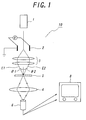
- Fig. 1 is a structural view schematically showing a transmission electron microscope according to the present invention.
- the transmission electron microscope (TEM) 10 illustrated in Fig. 1 includes an electron beam source 1, a deflection plate 2, an irradiation lens 3, a focusing lens 4 and an imaging device 6 which are provided in front of the electron beam source 1.
- the imaging device 6 is connected to a stereo displaying monitor 8.
- a sample "S" to be observed is disposed in between the irradiation lens 3 and the focusing lens 4.
- An electron beam from the electron beam source 1 is deflected in the left direction by applying a given voltage to the deflection plate 2 when the electron beam is passed through the deflection plate 2 to form a first electron beam E1, which is incident onto a given portion of the sample S by an angle of ⁇ 1. Then, the polarity of the voltage to be applied to the deflection plate 2 is switched to deflect the electron beam from the electron beam source 1 in the right direction and to form a second electron beam E2, which is incident onto the portion of the sample S by an angle of ⁇ 2.
- the first electron beam E1 and the second electron beam E2 are passed through the sample S.
- a first image of the sample S by the first electron beam E1 and a second image of the sample S by the second electron beam E2 are incident to and passed through the focusing lens 4, and incident into the imaging device 6.
- electric signals corresponding to the first image and the second image are transmitted to the stereo displaying monitor 8, where the first image and the second image are combined to generate a three-dimensional image of the portion of the sample S with the first electron beam E1 and the second electron beam E2 being incident.
- the sample can be observed three-dimensionally.
- the tact time in observation of the sample S depends on the time interval in incidence between the first electron beam E1 and the second electron beam E2 for the sample S, and more, corresponds to the switching interval of the polarity of voltage for the deflation plate 2. Therefore, if the switching interval is synchronized with an external signal, it can be reduced extremely short, for example up to the order of centisecond. As a result, the sample S can be observed in real-time.
- the switching interval can be synchronized with an operation signal for the imaging device 6.
- the first image by the first electron beam E1 and the second image by the second electron beam E2 can be easily introduced into the imaging device 6 at every frame. Therefore, the introduction of the first image and the second image in the same frame at the same time can be prevented, and the non-introduction of the first image or the second image in a given frame can be prevented, so that the sample can be precisely observed three-dimensionally.
- the incident angle ⁇ 1 of the first electron beam E1 for the sample S is preferably set within a range of one to five degrees from a normal line of the sample S.
- the incident angle ⁇ 2 of the second electron beam E2 for the sample S is preferably set within a range of one to five degrees from the normal line of the sample S. In this case, the three-dimensional image of the portion of the sample S can be precisely obtained and as a result, the sample S can be precisely observed three-dimensionally.
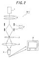
- Fig. 2 is a structural view schematically showing another transmission electron microscope which is modified from the one in Fig. 1.
- the irradiation lens 3 is disposed in between the deflection plate 2 and the sample S
- the irradiation lens 3 is disposed in between the electron beam source 1 and the deflection plate 2.
- the electron beam from the electron beam source 1 is deflected by only the single deflection plate 2 when the irradiation lens 3 is disposed in between the deflection plate 2 and the sample S, but by the two deflection plates 2-1 and 2-2 when the irradiation lens 3 is disposed in between the electron beam source 1 and the deflection plate 2.
- the TEM 10 is desired.
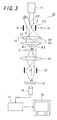
- Fig. 3 is a structural view schematically showing still another transmission electron microscope according to the present invention.
- the TEM 20 illustrated in Fig. 3 includes an electron beam source 11, an electron beam trapezoidal prism 12, an irradiation lens 13, a focusing lens 14, an electron beam biprism 15 and an imaging device 16 which are provided in front of the electron beam source 11.
- the imaging device 16 is connected to a stereo displaying monitor 18 via a separative and regenerative circuit 17.
- a sample "S" to be observed is disposed in between the irradiation lens 13 and the focusing lens 14.
- the focusing lens 14 and the electron beam biprism 15 constitute a focusing lens system.
- Fig. 4 is a structural view schematically showing the electron beam trapezoidal prism 12.
- the electron beam trapezoidal prism 12 includes a pair of filaments 122 and a pair of earth electrodes 123 provided in the outside of the filaments 122.
- a trapezoidal electric potential distribution is formed by the filaments 122 and the earth electrodes 123.
- an electron beam is not deflected when passed through the region A in between the filaments 122, and deflected by an electric field when passed through the regions B in between the filaments 122 and the earth electrodes 123.
- an electron beam from the electron beam source 11 is deflected in the left direction by an electric field generated in between the filaments 122 and the earth electrodes 123 when passing through the regions B of the electron beam trapezoidal prism 12 to form a first electron beam E1, which is incident onto a given portion of the sample S by an angle of ⁇ 1.
- the polarity of the voltage to be applied to the filaments 122 and the earth electrodes 123 is switched to deflect the electron beam from the electron beam source 11 in the right direction when passing through the regions B of the electron beam trapezoidal prism 12 to form a second electron beam E2, which is incident onto the portion of the sample S by an angle of ⁇ 2.
- the first electron beam E1 and the second electron beam E2 are passed through the sample S.
- a first image of the sample S by the first electron beam E1 and a second image of the sample S by the second electron beam E2 are incident to and passed through the focusing lens 14, and incident into the electron beam biprism 15.
- a third electron beam E3 from the electron beam source 11 is incident into the electron beam biprism 15 via the focusing lens 14, not through the sample S.
- the first and the second images are superimposed as object waves with the third electron beam E3 as a reference wave to form electron beam holograms "H".
- the tact time in observation of the sample S depends on the time interval in incidence between the first electron beam E1 and the second electron beam E2 for the sample S, and more, corresponds to the switching interval of the polarity of voltage for the filaments 122 and the earth electrodes 123 of the electron beam trapezoidal prism 12. Therefore, if the switching interval is synchronized with an external signal, it can be reduced extremely short, for example up to the order of centisecond. As a result, the sample S can be observed in real-time.
- the switching interval can be synchronized with an operation signal for the imaging device 6, so that the above-mentioned effect in the first embodiment relating to Fig. 1 can be provided.
- a new apparatus and a new method whereby a laser beam of high intensity can be obtained through the condensation of a pulsed laser without a complicated optical system can be provided.
Landscapes
- Chemical & Material Sciences (AREA)
- Analytical Chemistry (AREA)
- Analysing Materials By The Use Of Radiation (AREA)
Applications Claiming Priority (2)
| Application Number | Priority Date | Filing Date | Title |
|---|---|---|---|
| JP2002336392 | 2002-11-20 | ||
| JP2002336392A JP3785458B2 (ja) | 2002-11-20 | 2002-11-20 | 透過型電子顕微鏡及び立体観察法 |
Publications (1)
| Publication Number | Publication Date |
|---|---|
| EP1426998A2 true EP1426998A2 (de) | 2004-06-09 |
Family
ID=32310629
Family Applications (1)
| Application Number | Title | Priority Date | Filing Date |
|---|---|---|---|
| EP03257301A Withdrawn EP1426998A2 (de) | 2002-11-20 | 2003-11-19 | Transmissionselektronenmikroskop und Verfahren zur dreidimensionalen Beobachtung |
Country Status (3)
| Country | Link |
|---|---|
| US (1) | US7012253B2 (de) |
| EP (1) | EP1426998A2 (de) |
| JP (1) | JP3785458B2 (de) |
Cited By (3)
| Publication number | Priority date | Publication date | Assignee | Title |
|---|---|---|---|---|
| EP2091064A1 (de) * | 2008-02-15 | 2009-08-19 | Hitachi Ltd. | Elektronenstrahlvorrichtung |
| EP2315232A3 (de) * | 2009-08-07 | 2014-04-23 | Hitachi, Ltd. | Transmissionselektronenmikroskop und Verfahren zur Untersuchung einer Probe |
| EP3376522A1 (de) * | 2017-03-14 | 2018-09-19 | Technische Universität Berlin | Verfahren und vorrichtung zur durchführung einer zeitaufgelösten interferometrischen messung |
Families Citing this family (9)
| Publication number | Priority date | Publication date | Assignee | Title |
|---|---|---|---|---|
| JP4512180B2 (ja) | 2004-01-09 | 2010-07-28 | 独立行政法人理化学研究所 | 干渉装置 |
| JP4512183B2 (ja) * | 2004-03-31 | 2010-07-28 | 独立行政法人理化学研究所 | 電子線干渉装置 |
| WO2006088159A1 (ja) * | 2005-02-21 | 2006-08-24 | National University Corporation Kyoto Institute Of Technology | 電子顕微鏡及び複合照射レンズ |
| US9008378B2 (en) * | 2006-12-20 | 2015-04-14 | The Board Of Trustees Of The Leland Stanford Junior University | Arrangement and imaging of biological samples |
| EP2193360B1 (de) * | 2007-09-25 | 2014-11-05 | Centre National De La Recherche Scientifique | Verfahren und system zur messung nanoskaliger verformungen |
| US20120241612A1 (en) * | 2009-12-11 | 2012-09-27 | Hitachi Ltd | Electron Beam Biprism Device and Electron Beam Device |
| JP5934965B2 (ja) * | 2012-04-26 | 2016-06-15 | 国立研究開発法人理化学研究所 | 電子線装置 |
| CN114002240A (zh) * | 2021-09-27 | 2022-02-01 | 中国科学院广州地球化学研究所 | 一种地质样品微结构的电子显微三维重构表征方法 |
| JP7642524B2 (ja) * | 2021-12-24 | 2025-03-10 | 株式会社日立製作所 | 干渉走査透過型電子顕微鏡 |
Family Cites Families (5)
| Publication number | Priority date | Publication date | Assignee | Title |
|---|---|---|---|---|
| JPS4922576B1 (de) | 1970-04-30 | 1974-06-10 | ||
| DE2541245A1 (de) * | 1975-09-12 | 1977-03-24 | Siemens Ag | Korpuskularstrahl-rastermikroskop |
| JPH01264151A (ja) | 1988-04-15 | 1989-10-20 | Hitachi Ltd | 荷電粒子線装置における複数ビーム発生装置 |
| JPH03246861A (ja) | 1990-02-23 | 1991-11-05 | Nec Corp | 透過型電子顕微鏡 |
| US5576543A (en) * | 1995-08-21 | 1996-11-19 | Texsem Laboratories, Inc. | Method and apparatus for determining crystallographic characteristics |
-
2002
- 2002-11-20 JP JP2002336392A patent/JP3785458B2/ja not_active Expired - Lifetime
-
2003
- 2003-11-17 US US10/713,109 patent/US7012253B2/en not_active Expired - Fee Related
- 2003-11-19 EP EP03257301A patent/EP1426998A2/de not_active Withdrawn
Cited By (6)
| Publication number | Priority date | Publication date | Assignee | Title |
|---|---|---|---|---|
| EP2091064A1 (de) * | 2008-02-15 | 2009-08-19 | Hitachi Ltd. | Elektronenstrahlvorrichtung |
| US7923685B2 (en) | 2008-02-15 | 2011-04-12 | Hitachi, Ltd. | Electron beam device |
| EP2315232A3 (de) * | 2009-08-07 | 2014-04-23 | Hitachi, Ltd. | Transmissionselektronenmikroskop und Verfahren zur Untersuchung einer Probe |
| EP3376522A1 (de) * | 2017-03-14 | 2018-09-19 | Technische Universität Berlin | Verfahren und vorrichtung zur durchführung einer zeitaufgelösten interferometrischen messung |
| WO2018166786A1 (en) * | 2017-03-14 | 2018-09-20 | Technische Universität Berlin | Method and apparatus for carrying out a time-resolved interferometric measurement |
| US11293747B2 (en) | 2017-03-14 | 2022-04-05 | Technische Universitaet Berlin | Method and apparatus for carrying out a time-resolved interferometric measurement |
Also Published As
| Publication number | Publication date |
|---|---|
| US7012253B2 (en) | 2006-03-14 |
| JP2004171922A (ja) | 2004-06-17 |
| US20040144923A1 (en) | 2004-07-29 |
| JP3785458B2 (ja) | 2006-06-14 |
Similar Documents
| Publication | Publication Date | Title |
|---|---|---|
| US7012253B2 (en) | Transmission electron microscope and three-dimensional observing method | |
| US8193494B2 (en) | Transmission electron microscope and method for observing specimen image with the same | |
| WO2011018932A1 (ja) | 荷電粒子線装置及び画像表示方法 | |
| US2528510A (en) | Color television | |
| US4719482A (en) | Three-dimensional color television | |
| US3585382A (en) | Stereo-scanning electron microscope | |
| JP2661908B2 (ja) | エネルギー選択可視化装置 | |
| JPS5854784Y2 (ja) | 立体走査電子顕微鏡 | |
| US3986027A (en) | Stereo scanning microprobe | |
| JP2001229868A (ja) | ホログラフィ電子顕微鏡 | |
| JP2887361B2 (ja) | 透過電子顕微鏡用又は電子エネルギー損失分析電子顕微鏡用の撮像方法及び撮像装置 | |
| JPH08266535A (ja) | X線装置 | |
| JP2983832B2 (ja) | 立体映像表示装置 | |
| GB1300624A (en) | Charged particle beam apparatus having means to observe a stereo-image of a specimen | |
| JPH0541195A (ja) | 走査型電子顕微鏡装置 | |
| JPS62252055A (ja) | 立体視電子顕微鏡 | |
| JPH05191838A (ja) | 三次元情報記録再生装置 | |
| JPH10224821A (ja) | 複眼カメラおよびその複眼カメラを用いた映像表示システム | |
| DE19860224A1 (de) | Verfahren zur Erzeugung von Echtzeit-Stereobildern von Werkstoffproben mittels Teilchenstrahl-Rastermikroskop | |
| JPH06310070A (ja) | 走査型電子顕微鏡およびその類似装置 | |
| JPS61233950A (ja) | 電子顕微鏡 | |
| JP2000081400A (ja) | 光電子顕微鏡装置 | |
| JPH07234378A (ja) | 立体映像表示装置 | |
| JP2953085B2 (ja) | 観察装置 | |
| JP3360395B2 (ja) | X線tv装置 |
Legal Events
| Date | Code | Title | Description |
|---|---|---|---|
| PUAI | Public reference made under article 153(3) epc to a published international application that has entered the european phase |
Free format text: ORIGINAL CODE: 0009012 |
|
| 17P | Request for examination filed |
Effective date: 20031215 |
|
| AK | Designated contracting states |
Kind code of ref document: A2 Designated state(s): AT BE BG CH CY CZ DE DK EE ES FI FR GB GR HU IE IT LI LU MC NL PT RO SE SI SK TR |
|
| AX | Request for extension of the european patent |
Extension state: AL LT LV MK |
|
| STAA | Information on the status of an ep patent application or granted ep patent |
Free format text: STATUS: THE APPLICATION IS DEEMED TO BE WITHDRAWN |
|
| 18D | Application deemed to be withdrawn |
Effective date: 20060601 |