EP1427009A1 - Procede d'evaluation de la forme d'une plaquette, plaquette et procede de selection de plaquette - Google Patents
Procede d'evaluation de la forme d'une plaquette, plaquette et procede de selection de plaquette Download PDFInfo
- Publication number
- EP1427009A1 EP1427009A1 EP02765447A EP02765447A EP1427009A1 EP 1427009 A1 EP1427009 A1 EP 1427009A1 EP 02765447 A EP02765447 A EP 02765447A EP 02765447 A EP02765447 A EP 02765447A EP 1427009 A1 EP1427009 A1 EP 1427009A1
- Authority
- EP
- European Patent Office
- Prior art keywords
- wafer
- peripheral portion
- configuration
- region
- evaluating
- Prior art date
- Legal status (The legal status is an assumption and is not a legal conclusion. Google has not performed a legal analysis and makes no representation as to the accuracy of the status listed.)
- Withdrawn
Links
Images


Classifications
-
- G—PHYSICS
- G01—MEASURING; TESTING
- G01B—MEASURING LENGTH, THICKNESS OR SIMILAR LINEAR DIMENSIONS; MEASURING ANGLES; MEASURING AREAS; MEASURING IRREGULARITIES OF SURFACES OR CONTOURS
- G01B11/00—Measuring arrangements characterised by the use of optical techniques
- G01B11/24—Measuring arrangements characterised by the use of optical techniques for measuring contours or curvatures
-
- H—ELECTRICITY
- H10—SEMICONDUCTOR DEVICES; ELECTRIC SOLID-STATE DEVICES NOT OTHERWISE PROVIDED FOR
- H10P—GENERIC PROCESSES OR APPARATUS FOR THE MANUFACTURE OR TREATMENT OF DEVICES COVERED BY CLASS H10
- H10P74/00—Testing or measuring during manufacture or treatment of wafers, substrates or devices
Definitions
- the present invention relates to a method for evaluating a configuration of a wafer represented by a silicon wafer, a wafer suitable for an exposure system and a sorting method for a good quality wafer.
- SFQR Site Front Least Square Range
- a size of the site is generally 20 mm square or 25 mm square.
- Improvements have also been realized on precision, etc. of an exposure system along with the progress of the high integration level as described above, while troubles have frequently occurred that the exposure system stops in the course of patterning on a wafer.
- a method for evaluating a wafer configuration of the present invention comprises the following steps of: obtaining plural wafer configuration profiles of from the central portion of a wafer to the edge portion thereof along the entire periphery thereof at a prescribed angular space; providing a first region for calculating a reference line for each of the profiles in the central side of the wafer; calculating the reference line in the first region; further providing a second region in the peripheral side of the wafer outside the first region; extrapolating the reference line calculated in the first region to the second region; analyzing a value (an actually measured value - a reference value) obtained by subtracting the reference line (the reference value) in the second region from a configuration (the actually measured value) in the second region; calculating the maximum value among the values as a surface characteristic A and the minimum value among the values as a surface characteristic B; and evaluating configuration uniformity in the peripheral portion of the wafer from plural surface characteristics A and surface characteristics B obtained along the entire peripheral portion of the wafer.
- a wafer surface is divided into areas (sites) each about 20 mm square or about 25 mm square in which a reference plane is prepared for evaluation, but in this case, since a reference plane is prepared in a narrow area, the SFQR was averaged within the plane; it is often impossible to perform exact evaluation on deterioration of an actual configuration or the like. Especially, in this conventional evaluating method, a configuration of the peripheral portion of the wafer cannot be evaluated accurately.
- a surface characteristic A (hereinafter also referred to as A parameter) and a surface characteristic B (hereinafter also referred to as B parameter) obtained by the method for evaluating a wafer configuration according to the present invention can preferably perform very exact evaluation of a surface configuration in the peripheral portion of the wafer.
- a parameter a surface characteristic A obtained along the peripheral portion of the wafer as performed in the present invention
- configuration uniformity in the peripheral portion of the wafer can be evaluated.
- this configuration uniformity in the peripheral portion is referred to as B parameter peripheral portion uniformity.
- a difference between the surface characteristic A and the surface characteristic B (a surface characteristic (A - B)) is obtained from each of the profiles in advance, and the configuration uniformity in the peripheral portion of the wafer is evaluated from a difference between the maximum value and the minimum value of the plural surface characteristics (A - B) obtained in the wafer surface (this configuration uniformity in the peripheral portion of the wafer is hereinafter referred to as (A - B) parameter peripheral portion uniformity).
- the configuration uniformity in the peripheral portion of the wafer may be evaluated with standard deviations of plural surface characteristics A, surface characteristics B or differences therebetween (surface characteristics (A - B)) obtained in the peripheral portion of the wafer as variations.
- the wafer configuration measured with a prescribed space within the wafer surface is displacement (height or roughness) in the direction vertical to the wafer surface or a wafer thickness. Evaluation on the displacement in the direction vertical to the wafer surface makes it possible to perform evaluation based on the front side reference. Further, evaluation on the wafer thickness makes it possible to perform evaluation based on the back side reference.
- the prescribed space described above is preferably 1 mm or less (but in excess of 0 mm).
- the prescribed angular space to obtain wafer configuration profiles is preferably 1 degree or less (but in excess of 0 degree).
- an index for the configuration uniformity in the peripheral portion of the wafer can be obtained by attaining plural surface characteristics A and surface characteristics B along the entire periphery (along the peripheral portion of the wafer).
- a reference line is prepared in a global (extensive) region (a first region) for calculating a reference line from a wafer configuration (each of profiles), and the reference line is used by being extrapolated to a region (a second region) to be evaluated such as the peripheral portion of the wafer for analyzing the surface characteristics of the second region, the surface characteristics of the region being evaluated.
- a region a second region
- Measuring a value obtained by subtracting the reference line from the actual configuration (an actually measured value - a reference value) the calculated maximum value is evaluated as a rise (A in FIG. 1) and the calculated minimum value as a sag (B in FIG. 1).
- a reference line is prepared in an extensive specified region (a first region) on a wafer surface, which is an area larger than the site size to be evaluated by the SFQR or the like; the surface characteristics in a region to be evaluated (a second region) other than the first region is evaluated based on the reference line prepared in the extensive specified region (the first region).
- a wafer most suitable for an exposure system can be defined by performing the method for evaluating a wafer configuration of the present invention.
- a yield in the exposure system (such as a misalignment occurrence frequency in a device pattern) is mainly due to the surface characteristic A.
- an average value of its surface characteristics A is smaller than 150 nm.
- a wafer most suitable for the exposure system has the difference of 600 nm or less.
- a wafer suitable for the exposure system has the difference between the maximum value and the minimum value of plural surface characteristics (A - B) obtained within the wafer surface (the (A - B) parameter peripheral portion uniformity) of preferably 500 nm or less and more preferably 400 nm or less.
- the wafer described above has not extreme sags and local sags in the peripheral portion of the wafer when evaluated with the surface characteristics A and B.
- sorted wafers each having a difference between the maximum value and the minimum value of the obtained plural surface characteristics (A - B) (the (A - B) parameter peripheral portion uniformity) of 500 nm or less, the sorted wafers being used in an exposure system. More preferably, there are sorted wafers each having a difference between the maximum value and the minimum value of the obtained plural surface characteristics (A - B) (the (A - B) parameter peripheral portion uniformity) of 400 nm or less, the sorted wafers being used in an exposure system.
- wafers are sorted and the sorted wafers are used in an exposure system; abnormal stops or the like of the exposure system may be remarkably reduced.
- FIG. 2 shows schematically a configuration of a wafer W.
- a peripheral edge portion of the wafer W is chamfered to prevent cracking or the like, a chamfered portion Wm being formed.
- this chamfered portion Wm is ignored in evaluating a wafer configuration, and out of an object of measurement.
- Evaluating a wafer configuration is often performed on a region of a main surface Wn of the wafer W which is formed by excluding an area with the width of about 3 mm or about 2 mm from the chamfered portion Wm of the wafer W.
- a region which is formed by excluding an area with the width of 1mm from the chamfered portion or the region to the very limit of the boundary between the main surface and the chamfered portion. Therefore, while there is no limitation on the evaluation region (especially, the excluding area), considering measuring precision and the analyzed data precision, in the present state it is preferable to evaluate the region formed by excluding an area with the width of about 1mm.
- FIG. 1 schematically shows displacement in thickness of a surface of the wafer W.
- a main purpose of the method for evaluating a wafer configuration according to the present invention is to quantify rises or sags which are easily generated on an area with the width of about 10 mm of the peripheral portion of the wafer (10 mm from the chamfered portion Wm).
- a reference line 10 is prepared within an extensive region (a first region) W1 for calculating the reference line in a wafer surface from the basic configuration of the wafer W; the reference line 10 is extrapolated to a region (a second region) W2 to be evaluated on the peripheral portion of the wafer, and is used thereon for analyzing the surface characteristics of the second region W2 for analyzing the surface characteristics of the region W2.
- a value (an actually measured value - a reference value) obtained by subtracting the reference line 10 (a reference value) from an actual configuration (an actually measured value) of the wafer is measured, and the measured maximum value is evaluated as rises A, the measured minimum value being evaluated as sags B.
- Wc is a central portion of a wafer
- We is an edge portion of the wafer
- X is a boundary between the first region W1 and the second region W2, which is provided at an arbitrary position.
- a configuration of a wafer is measured with a prescribed space on a surface of the wafer; the measured wafer configuration is successively stored; a configuration profile of from the central portion We of the wafer W to the edge portion We thereof as shown in FIG. 3 is obtained from the stored configuration; there is calculated a reference line up to a boundary X of the first region W1 provided at an arbitrary position away from the central portion (in the radial direction of the wafer); and then a difference between a configuration (an actually measured value) at an arbitrary position (in the direction of the wafer thickness) and a value (a reference value)of the reference line 10 at this position is analyzed to be calculated as the surface characteristics.
- the prescribed measurement space on the wafer surface should be preferably within 1 mm.
- the space is naturally more than 0 mm, but by performing evaluation with the smallest possible space, more accurate configuration can be quantified.
- the reference line may be approximated by a straight line or a curved line most well reflecting a configuration of the central portion of the wafer W, but usually the central portion of the wafer W is polished to a high flatness level, so that the reference line is fully approximated by the straight line.
- an arbitrary position X of a boundary between the first region W1 and the second region W2 is preferably provided at an arbitrary position in the radial direction of the wafer W and in an area (an area where the first region is as extensive as possible) of the wafer W where no peripheral sag nor rise is generated.
- usually sags and the like occur in the area outside of about 10 mm away from the peripheral edge of the wafer, so that the arbitrary position (boundary) X should preferably be provided at a position of about 30 mm away from the peripheral edge of the wafer.
- a reference line or a reference plane at a position of 70 mm away from the central portion of the wafer in the case of an 8 inch wafer (200 mm in diameter) and at a position of 120 mm away from the central portion in the case of a 12 inch wafer (300 mm in diameter).
- this position may be freely changed so that the wafer quality can be evaluated most accurately.
- a configuration profile of a wafer W of from the central portion Wc to the edge portion We is obtained; a reference line of from the central portion Wc to an arbitrary position X is calculated; then there is analyzed a value obtained by subtracting a reference line at an arbitrary position in the range of from the arbitrary position X to the edge portion We from a configuration at this position [a configuration at. an arbitrary position (an actually measured value) - a reference line at an arbitrary position (a reference value)]; and the maximum value among the analyzed values (usually the positive maximum displacement amount or the maximum thickness difference) is calculated as the surface characteristic A (rises).
- This surface characteristic A quantitatively indicates a rising configuration on the peripheral portion of the wafer.
- a configuration profile of from the central portion Wc of the wafer W to the edge portion We is obtained; a reference line of from the central portion to an arbitrary position X is calculated; then there is analyzed a value obtained by subtracting a reference line at an arbitrary position in the range of from the arbitrary position X to the edge portion We from a configuration at this position [a configuration at an arbitrary position (an actually measured value) - a reference line at an arbitrary position (a reference value)]; and the minimum value among the analyzed values (usually the negative maximum value) is calculated as the surface characteristic B (sags).
- This surface characteristic B quantitatively indicates a sagging configuration on the peripheral portion of the wafer.
- plural surface characteristics A and B are obtained along the wafer peripheral portion. It is especially preferable to analyze a configuration profile radially along about 400 lines (at an angular space of about 1 degree or less) within the wafer surface. While the value of the angular space is naturally in excess of 0 degree, very exact evaluation can be performed in the wafer peripheral portion with the angular space of 1 degree or less. Note that it is preferable to perform evaluation excluding parts including a notch, an orientation flat and a letter printed with a laser mark because the parts cause abnormal data easily.
- evaluation can be performed than in a conventional wafer configuration evaluation by using surface characteristics A and B.
- evaluation can be performed on configuration uniformity in the wafer peripheral portion by analyzing surface characteristics A and B along the wafer peripheral portion.
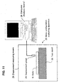
- FIG. 11 is a schematic explanatory view showing an essential structure of the apparatus for evaluating wafer configuration according to the present invention.
- An apparatus 20 for evaluating a wafer configuration shown in FIG. 11 is an apparatus used for measurement and analysis of displacement of a surface of a wafer W, which comprises a test stand 22, and a displacement measuring unit 26 having a displacement gauge 24 equipped with a laser oscillator or an automatic focusing mechanism, a computer 28, etc., and optically measures shifts in the distance from the previously calibrated reference point as the displacement.
- the displacement measuring unit 26 functions as a configuration measuring unit.
- the test stand 22 is a stand used for placing thereon a silicon wafer W as an object to be measured.
- the displacement gauge 24 is an apparatus for irradiating a laser beam with a prescribed space onto a surface of a silicon wafer W placed on the test stand 22, and for instance, a HeNe laser or the like is used as the laser beam.
- the displacement gauge 24 is equipped with an automatic focusing mechanism (not shown), and this automatic focusing mechanism is provided with, for instance, a CCD (Charge Coupled Device) camera (not shown), an automatic focusing circuit (not shown), and others, and can automatically focus on an image reflected from the silicon wafer of the laser beam which is emitted from the laser oscillator.
- CCD Charge Coupled Device
- the displacement gauge 24 measures the displacement from a reference point when focused by the automatic focusing mechanism, and inputs the displacement data into the computer 28.
- the computer 28 is equipped with a CPU (Central Processing Unit), an RAM (Random Access Memory), an ROM (Read Only Memory), etc.
- the computer 28 into which the displacement data output from the displacement gauge 24 are input, reads the analysis program stored in the ROM using the RAM as a work area, and calculates the surface characteristics A and B of the wafer quality according to the present invention from the input displacement data with the CPU.
- the surface characteristics are parameters especially used for evaluation of a peripheral portion of the wafer.
- the computer 28 comprises a storage means for successively inputting and storing configuration data obtained by the displacement measuring unit (the configuration measuring unit) 26, and a surface characteristic calculating unit for reading a configuration data (an actually measured value) of from the central portion of the wafer W to the edge portion thereof from the storage device, calculating a reference line (a reference value) from the central portion of the wafer to an arbitrary portion, then analyzing a value (an actually measured value - a reference value) obtained by subtracting the reference line or the reference plane from an arbitrary position, and calculating the analyzed difference as the surface characteristics.
- FIG. 12 is a schematic explanatory view showing an essential structure of another embodiment of the apparatus for evaluating a wafer configuration according to the present invention.
- a thickness may be measured with a flatness measuring unit based on an electrostatic capacitance system in place of displacement of the wafer surface.
- the flatness measuring unit based on the electrostatic capacitance system is used as a thickness measurement unit 34 equipped with a thickness gauge 32 comprising electrostatic capacitance type of upper and lower sensors 32a, 32b arranged such that the wafer W is held between them as shown in FIG. 12. and measures the thickness of the wafer W by measuring the distances' between the sensors 32a, 32b and upper and lower surfaces of the wafer W, respectively.
- a commercial non-contact type of wafer thickness, flatness and BOW/WARP measuring unit such as Ultra Gauge 9900 produced by ADE Corp. may be used.
- the apparatus 30 for evaluating a wafer configuration shown in FIG. 12 comprises a wafer holding jig 36 for holding a wafer W, the above mentioned thickness measuring unit 34, and a computer 28, and is used for measuring a thickness of the wafer W.
- the thickness measuring unit 34 functions as a configuration measuring unit.
- any type of evaluating apparatus may be used without any specific limitation, provided that it can finely and accurately evaluate configurations (irregularities) of the wafer W.
- the surface characteristics A and B are evaluated on the basis of the displacement or thickness measured as described above.
- the reference line is a line calculated by means of the method of least squares and other methods. Therefore, as to the space with which data are to be sampled, the finer, the better. Specifically, a proper range for the space should be 1 mm or less.
- FIG. 1 is a view showing values for the surface characteristics A and B of a prescribed wafer, and a configuration profile on a cross section thereof.
- an equation for calculating the surface characteristics A and B is programmed for each profile.
- the analysis program is a software evaluating an average value, a standard deviation, a maximum value and a minimum value of plural surface characteristics A, B or (A - B) obtained from profiles along a peripheral portion of the wafer.
- thickness data of a mirror polished silicon wafer are read with an arbitrary space (about 1 mm) on the silicon wafer from the central portion thereof toward the edge portion; then a reference line is prepared using the thickness data in an extensive first region by means of the method of least squares; a difference between the reference line and a configuration in a second region to be evaluated is calculated, and the maximum value within the area is analyzed.
- thickness data of a mirror polished silicon wafer are read with an arbitrary space (about 1 mm) on the silicon wafer from the central portion thereof toward the edge portion; then a reference line is prepared using the thickness data in an extensive first region by means of the method of least squares; a value obtained by subtracting the reference line from a configuration in a second region to be evaluated is calculated, and the minimum value within the area is analyzed.
- the analysis described above is conducted on each profile along the peripheral portion of the wafer.
- uniformity (variation) of a configuration in the peripheral portion of the wafer is evaluated.
- evaluation is performed on an average value, a standard deviation, a maximum value, a minimum value and others of surface characteristics A and B or a difference between the surface characteristic A and the surface characteristic B (hereinafter may be referred to as a surface characteristic (A - B) or (A - B) parameter).
- a surface configuration of a wafer, especially a peripheral portion thereof can be evaluated accurately on the basis of a specific standard from 'a different viewpoint from the conventional techniques such as SFQR.
- SFQR conventional techniques
- evaluation on configuration uniformity of the wafer peripheral portion can be realized. It is possible to obtain more effective information as compared to the conventional evaluation for the wafer configuration, and hence problems in a device fabricating process such as a process using an exposure system and others can be solved.
- the surface characteristics can be fully used as parameters for analysis of various experimental data, too.
- the wafer thickness was measured at positions with a space of 0.95 mm on the whole surface of the wafer (excluding the chamfered portion of an area with 0.5 mm in width of the peripheral portion); the measured wafer thickness data were successively stored; configuration profiles of the wafer of from the central portion to the edge portion (98.5 mm away from the central portion) as shown in FIG.
- the surface characteristics A and B are the maximum value and minimum value in the second region to be evaluated 'of 70 mm to 98.5 mm, respectively
- FIG. 4 there are shown changes in A and B parameter values at evaluation positions for the evaluated surface characteristics.
- the abscissa of FIG. 4 indicates the evaluated position ⁇ .
- the position ⁇ is obtained by plotting values evaluated rotating the wafer in the range of 360 degrees in the clockwise direction at the notch as 0 degrees.
- the ordinate indicates the A and B parameter values in ⁇ m unit.
- a stepper (a common name of a stepping projection exposure system) was used in which the wafer is repeatedly stepped and exposed to a projected image of a mask pattern (a reticle pattern).
- a scanning exposure system As the exposure system, there may be used a scanning exposure system.
- the present inventors have seriously investigated the abnormal stop of the stepper and conceived that the stop may be greatly influenced by the uniformity in a peripheral portion of the B parameter obtained using the above method for evaluating the wafer configuration.
- evaluation was performed on an average value, a standard deviation, a maximum value, a minimum value and (a maximum value - a minimum value) of plural surface characteristics A, B or (A-B). Results of the evaluation are shown in Table 1. While changes (variations) in the parameter can be visually observed when the graph as shown in FIG. 4 is prepared, quantitative evaluation can also be performed by obtaining (the maximum value - the minimum value), the standard deviation and others. In the present invention, evaluation can be performed quantifying uniformity of the configuration in a peripheral portion of the wafer.
- the wafer manufacturing process comprises, a slicing step of slicing the single crystal ingot with a wire saw or the like to obtain a thin and disk-shaped wafer; a chamfering step of chamfering a peripheral edge portion of the wafer obtained through the slicing step to prevent cracking and chipping of the wafer; a lapping step of flattening this wafer; a flattening step of surface grinding or the like; an etching step that removes machining deformation remaining behind in the so chamfered and flattened wafer; a polishing step of making a mirror surface of the wafer; and a cleaning step of cleaning the polished wafer to remove an abrasive slurry or dust particles deposited thereon.
- the chamfering step it is to perform grinding and mirror-chamfering while taking care of uniformity in chamfering. For this end, it is to perform the chamfering so as to control uniformly a contact pressure of a grindstone, a buff or the like. It is also to control it with the number of rotation of the wafer and the grindstone (buff) or the like.
- the etching step it is to take care of uniformity of etching. Especially, the etching is performed controlling uniformly streams of the etchant. For this end, there is a method to control the speed of rotation of an etching drum and others. It is also to improve it by reducing a contact area between the etching drum supporting wafers and the wafers.
- the surface grinding step or the lapping step As an improvement in the surface grinding step or the lapping step, it is to machine the wafer controlling spark-out because work damages and the like are easily generated when a fixed grindstone or a lapping table are sparked out after the lapping is over.
- adjustment is made on a grain size of the grindstone, a rotation speed thereof, a feed speed thereof so as to generate grinding striations at the lowest level possible.
- a polishing pressure applied on a peripheral portion of a wafer in polishing that is a change in a size of a work holding plate, polishing such that the central portion of a work holding region is of a harder quality while a peripheral portion thereof is of a softer quality and the peripheral portion is vacuum-chucked; and a back surface coat is formed on a back surface of a work, the work is held via the back surface coat and a front surface of the work is polished, wherein thickness of the back surface coat is different between the peripheral portion and the central portion in polishing.
- peripheral sags can be controlled.
- a polishing method in which a pushing pressure applied on a work peripheral portion is controlled independently of the central portion by changing a polishing head.
- the above improving methods are combined mainly with a process including: a slicing step; a chamfering step; a surface grinding step; an etching step; a low damage lapping step; and a polishing step to obtain wafers S2, S3 and S4 manufactured by three different wafer manufacturing processes.
- the wafers were evaluated according to the method for evaluating a wafer configuration of the present invention to obtain graphs of FIG. 5 (wafer S2), FIG. 6 (wafer S3) and FIG.7 (wafer S4) in respect of the above three processes.
- a wafer configuration evaluation method is the same as in Example 1.
- uniformity of a peripheral portion in the surface characteristic (A - B) was 500 nm or less, that is 419 nm, 404 nm and 380 nm. These wafers S2, S3 and S4 were good in a process using a stepper.
- Wafer S2 (Example 2) 0.330 -0.007 0.337 0.110 0.079 Wafer S3 (Example 2) 0.241 -0.024 0.265 0.104 0.055 Wafer S4 (Example 2) 0.253 -0.020 0.272 0.093 0.060 Wafer S5 (Comparative Example 1) 0.105 -0.028 0.132 0.032 0.024 Wafer S1 0.135 -0.029 0.164 0.038 0.028
- the wafer manufacturing process comprises, a slicing step of slicing the single crystal ingot to obtain a thin and disk-shaped wafer; a chamfering step of chamfering a peripheral edge portion of the wafer obtained through the slicing step to prevent cracking and chipping of the wafer; a lapping step of flattening this wafer; an etching step that removes machining deformation remaining behind in the so chamfered and lapped wafer; a polishing step of making a mirror surface of the wafer; and a cleaning step of cleaning the polished wafer to remove an abrasive slurry or dust particles deposited thereon.
- the wafer manufactured from the common wafer manufacturing process was referred to as S5.
- Evaluation was performed on the wafer S5 according to the method for evaluating a wafer configuration of the present invention so as to obtain a graph as shown in FIG. 8. Furthermore, quantified evaluation results are additionally shown in Tables 2 to 4. A configuration evaluation method is the same as Example 1.
- the wafer S5 was loaded into a stepper with the result that abnormal stop of the stepper was observed at a rate of 100 %.
- a difference between the maximum value and the minimum value (the B parameter peripheral portion uniformity) of plural surface characteristics B obtained on a wafer was 682 nm.
- Uniformity of a peripheral portion in the surface characteristic (A - B) was 648 nm.
- Evaluation results of the wafer S1 evaluated in Example 1 are also additionally shown in Tables 2 to 4.
- Abnormal stop of the stepper was also observed with the wafer S1.
- the wafers S1 and S5 were poor in a process using the stepper. It is found that a local change in the B parameter exerts a large influence on stop of the apparatus.
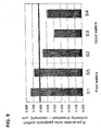
- wafers S1 to S5 there are shown the peripheral portion uniformity (the maximum value - the minimum value) in the B parameter in FIG.9 and the peripheral portion uniformity (the maximum value - the minimum value) in the (A-B) parameter in FIG.10. It is found that a wafer with the B parameter peripheral portion uniformity of 600 nm or less is good and a wafer with the (A - B) parameter peripheral portion uniformity of 500 nm or less is good.
- the B parameter uniformity was not able to be reduced to be perfectly 600 nm or less. Accordingly, wafers were evaluated according to the configuration evaluation method of the present invention to sorted wafers within the scope of the present invention and thereafter, the sorted wafers were loaded into a device process. To be concrete, wafers having the surface characteristic B peripheral portion uniformity of 600 nm or less (these wafers had the surface characteristic (A - B) peripheral portion uniformity of 400 nm or less) were loaded into a stepper process and operations of the stepper were observed. As a result, it was confirmed that the stepper was not stopped at all.
- Wafers manufactured in a common wafer manufacturing process were loaded into a stepper process without sorting of the wafers. As a result, abnormal stop of the stepper was observed. Stop of the apparatus occurred at a frequency of the order of 10 % of processed wafers. Evaluation on a wafer causing abnormality according to the present invention shows that the wafer peripheral portion uniformity in the surface characteristic B was 600 nm or more. Moreover, the wafer peripheral portion uniformity in the surface characteristic (A - B) (the maximum value - the minimum value) was also 600 nm or more. Note that abnormal stop occurred or did not occur for wafers having the peripheral portion uniformity in the surface characteristic B of the order in the range of 500 nm to 700 nm.
- the peripheral portion uniformity in the B parameter is especially important and it is found that abnormal stop of the apparatus is reduced using wafers with (the maximum value - the minimum value) of 600 nm or less among the peripheral portion configuration uniformity.
- wafers with (the maximum value - the minimum value) in the (A - B) parameter uniformity of 400 nm or less stop of the apparatus is greatly reduced, resulting in improvement on a product yield as well.
- Displacement or a thickness measured with a prescribed space using a displacement or thickness measuring means can define a wafer configuration more precisely by using a surface characteristic calculating means than a conventional index indicating flatness such as SFQR. Especially, since the peripheral portion uniformity in the B parameter can be quantitatively evaluated, it can be determined surely whether a wafer is good or poor on a prescribed criterion.
- evaluation can be more precisely than conventional wafer configuration evaluation and hence abnormality in a device process is prevented, resulting in improvement on a product yield.
Landscapes
- Physics & Mathematics (AREA)
- General Physics & Mathematics (AREA)
- Testing Or Measuring Of Semiconductors Or The Like (AREA)
- Length Measuring Devices By Optical Means (AREA)
Applications Claiming Priority (3)
| Application Number | Priority Date | Filing Date | Title |
|---|---|---|---|
| JP2001280500 | 2001-09-14 | ||
| JP2001280500A JP3838341B2 (ja) | 2001-09-14 | 2001-09-14 | ウェーハの形状評価方法及びウェーハ並びにウェーハの選別方法 |
| PCT/JP2002/009096 WO2003025999A1 (fr) | 2001-09-14 | 2002-09-06 | Procede d'evaluation de la forme d'une plaquette, plaquette et procede de selection de plaquette |
Publications (1)
| Publication Number | Publication Date |
|---|---|
| EP1427009A1 true EP1427009A1 (fr) | 2004-06-09 |
Family
ID=19104484
Family Applications (1)
| Application Number | Title | Priority Date | Filing Date |
|---|---|---|---|
| EP02765447A Withdrawn EP1427009A1 (fr) | 2001-09-14 | 2002-09-06 | Procede d'evaluation de la forme d'une plaquette, plaquette et procede de selection de plaquette |
Country Status (7)
| Country | Link |
|---|---|
| US (1) | US6975960B2 (fr) |
| EP (1) | EP1427009A1 (fr) |
| JP (1) | JP3838341B2 (fr) |
| KR (1) | KR100796858B1 (fr) |
| CN (1) | CN1253934C (fr) |
| TW (1) | TW559932B (fr) |
| WO (1) | WO2003025999A1 (fr) |
Families Citing this family (31)
| Publication number | Priority date | Publication date | Assignee | Title |
|---|---|---|---|---|
| US7197178B2 (en) * | 2003-07-14 | 2007-03-27 | Rudolph Technologies, Inc. | Photoresist edge bead removal measurement |
| US8489990B2 (en) * | 2005-03-02 | 2013-07-16 | Rovi Guides, Inc. | Playlists and bookmarks in an interactive media guidance application system |
| US7810383B2 (en) | 2005-04-08 | 2010-10-12 | Shin-Etsu Handotai Co., Ltd. | Method for evaluating semiconductor wafer, apparatus for evaluating semiconductor wafer, and method for manufacturing semiconductor wafer |
| US8135485B2 (en) * | 2007-09-28 | 2012-03-13 | Lam Research Corporation | Offset correction techniques for positioning substrates within a processing chamber |
| US8225683B2 (en) | 2007-09-28 | 2012-07-24 | Lam Research Corporation | Wafer bow metrology arrangements and methods thereof |
| JP5207447B2 (ja) * | 2008-01-31 | 2013-06-12 | Sumco Techxiv株式会社 | 半導体ウェーハの評価方法及び製造方法。 |
| US7976348B2 (en) * | 2008-05-07 | 2011-07-12 | Ortronics, Inc. | Modular insert and jack including moveable reactance section |
| US7601034B1 (en) | 2008-05-07 | 2009-10-13 | Ortronics, Inc. | Modular insert and jack including moveable reactance section |
| JP2010028011A (ja) * | 2008-07-24 | 2010-02-04 | Sumco Corp | エピタキシャル層の膜厚測定方法、エピタキシャルウェーハの製造方法およびエピタキシャルウェーハ製造工程管理方法 |
| KR200453608Y1 (ko) * | 2009-09-14 | 2011-05-16 | 허용 | 너트 일체형 배수관 |
| JP5862492B2 (ja) * | 2012-07-09 | 2016-02-16 | 信越半導体株式会社 | 半導体ウェーハの評価方法及び製造方法 |
| JP6007889B2 (ja) * | 2013-12-03 | 2016-10-19 | 信越半導体株式会社 | 面取り加工装置及びノッチレスウェーハの製造方法 |
| JP6191534B2 (ja) * | 2014-05-01 | 2017-09-06 | 信越半導体株式会社 | ウエハのそりの評価方法及びウエハの選別方法 |
| JP6508123B2 (ja) * | 2016-05-13 | 2019-05-08 | 信越半導体株式会社 | テンプレートアセンブリの選別方法及びワークの研磨方法並びにテンプレートアセンブリ |
| JP6443520B1 (ja) * | 2017-10-02 | 2018-12-26 | 株式会社Sumco | 半導体ウェーハの評価方法および該方法を用いた半導体ウェーハの製造方法 |
| CN112020764B (zh) * | 2018-04-13 | 2024-02-20 | 胜高股份有限公司 | 半导体晶片的评价方法和半导体晶片的制造方法 |
| KR20250012748A (ko) * | 2019-01-25 | 2025-01-24 | 램 리써치 코포레이션 | 통합된 웨이퍼 보우 측정들 |
| JP7103305B2 (ja) * | 2019-05-29 | 2022-07-20 | 信越半導体株式会社 | インゴットの切断方法 |
| US11393118B2 (en) * | 2019-06-18 | 2022-07-19 | Kla Corporation | Metrics for asymmetric wafer shape characterization |
| JP7172951B2 (ja) * | 2019-10-31 | 2022-11-16 | 信越半導体株式会社 | 半導体ウェーハの評価方法、半導体ウェーハの選別方法及びデバイスの製造方法 |
| US11177146B2 (en) | 2019-10-31 | 2021-11-16 | Applied Materials, Inc. | Methods and apparatus for processing a substrate |
| KR102457699B1 (ko) * | 2020-07-16 | 2022-10-24 | 에스케이실트론 주식회사 | 웨이퍼 및 그 형상 분석 방법 |
| KR102413432B1 (ko) * | 2020-08-28 | 2022-06-27 | 에스케이실트론 주식회사 | 웨이퍼 및 그 형상 분석 방법 |
| US12385850B2 (en) * | 2021-08-16 | 2025-08-12 | Globalwafers Co., Ltd. | Semiconductor wafers using front-end processed wafer global geometry metrics |
| JP7715094B2 (ja) * | 2022-07-25 | 2025-07-30 | 株式会社Sumco | 半導体ウェーハの評価方法 |
| CN115468737B (zh) * | 2022-08-10 | 2025-09-02 | 歌尔光学科技有限公司 | 投影光机解析力分级的确认方法、装置以及电子设备 |
| JP7729292B2 (ja) * | 2022-09-08 | 2025-08-26 | 株式会社Sumco | インゴットのvノッチ評価装置 |
| CN119816933A (zh) | 2022-09-12 | 2025-04-11 | 信越半导体株式会社 | 碎屑判定方法 |
| CN115717855B (zh) * | 2022-11-01 | 2026-03-13 | 上海中欣晶圆半导体科技有限公司 | 一种倒角加工规格纠错的方法 |
| CN117109481B (zh) * | 2023-07-28 | 2024-12-24 | 中国水利水电第五工程局有限公司 | 一种过流面混凝土整体平整度及过流能力检测评价方法 |
| CN117889773B (zh) * | 2024-03-15 | 2024-05-14 | 深圳市铨兴科技有限公司 | 一种晶圆翘曲形变测试设备 |
Family Cites Families (8)
| Publication number | Priority date | Publication date | Assignee | Title |
|---|---|---|---|---|
| US4510176A (en) * | 1983-09-26 | 1985-04-09 | At&T Bell Laboratories | Removal of coating from periphery of a semiconductor wafer |
| DE4224395A1 (de) * | 1992-07-23 | 1994-01-27 | Wacker Chemitronic | Halbleiterscheiben mit definiert geschliffener Verformung und Verfahren zu ihrer Herstellung |
| JP2000260840A (ja) | 1999-03-12 | 2000-09-22 | Toshiba Corp | 半導体基板の測定方法及び測定装置 |
| JP3491589B2 (ja) | 1999-12-22 | 2004-01-26 | 三菱住友シリコン株式会社 | 高平坦度半導体ウェーハの製造方法及び高平坦度半導体ウェーハ |
| US6852012B2 (en) * | 2000-03-17 | 2005-02-08 | Wafer Solutions, Inc. | Cluster tool systems and methods for in fab wafer processing |
| US6828163B2 (en) * | 2000-11-16 | 2004-12-07 | Shin-Etsu Handotai Co., Ltd. | Wafer shape evaluating method and device producing method, wafer and wafer selecting method |
| US6712673B2 (en) * | 2001-10-04 | 2004-03-30 | Memc Electronic Materials, Inc. | Polishing apparatus, polishing head and method |
| DE10159833C1 (de) * | 2001-12-06 | 2003-06-18 | Wacker Siltronic Halbleitermat | Verfahren zur Herstellung einer Vielzahl von Halbleiterscheiben |
-
2001
- 2001-09-14 JP JP2001280500A patent/JP3838341B2/ja not_active Expired - Lifetime
-
2002
- 2002-09-06 EP EP02765447A patent/EP1427009A1/fr not_active Withdrawn
- 2002-09-06 CN CNB028147316A patent/CN1253934C/zh not_active Expired - Lifetime
- 2002-09-06 US US10/488,689 patent/US6975960B2/en not_active Expired - Lifetime
- 2002-09-06 WO PCT/JP2002/009096 patent/WO2003025999A1/fr not_active Ceased
- 2002-09-06 KR KR1020037014805A patent/KR100796858B1/ko not_active Expired - Lifetime
- 2002-09-11 TW TW091120745A patent/TW559932B/zh not_active IP Right Cessation
Non-Patent Citations (1)
| Title |
|---|
| See references of WO03025999A1 * |
Also Published As
| Publication number | Publication date |
|---|---|
| CN1253934C (zh) | 2006-04-26 |
| CN1535476A (zh) | 2004-10-06 |
| US20040215418A1 (en) | 2004-10-28 |
| TW559932B (en) | 2003-11-01 |
| JP3838341B2 (ja) | 2006-10-25 |
| KR20040037279A (ko) | 2004-05-06 |
| WO2003025999A1 (fr) | 2003-03-27 |
| JP2003086646A (ja) | 2003-03-20 |
| US6975960B2 (en) | 2005-12-13 |
| KR100796858B1 (ko) | 2008-01-22 |
Similar Documents
| Publication | Publication Date | Title |
|---|---|---|
| US6975960B2 (en) | Method for evaluating wafer configuration, wafer, and wafer sorting method | |
| US6828163B2 (en) | Wafer shape evaluating method and device producing method, wafer and wafer selecting method | |
| JP4464033B2 (ja) | 半導体ウエーハの形状評価方法及び形状評価装置 | |
| US8231430B2 (en) | Wafer production method | |
| KR100887269B1 (ko) | 고정밀 에지 프로파일을 갖는 반도체 웨이퍼 및 반도체웨이퍼의 제작 방법 | |
| US8551346B2 (en) | Photomask-forming glass substrate and making method | |
| US20260063568A1 (en) | Systems and methods for processing semiconductor wafers using front-end processed wafer global geometry metrics | |
| JP4400331B2 (ja) | ウエーハの形状評価方法及び管理方法 |
Legal Events
| Date | Code | Title | Description |
|---|---|---|---|
| PUAI | Public reference made under article 153(3) epc to a published international application that has entered the european phase |
Free format text: ORIGINAL CODE: 0009012 |
|
| 17P | Request for examination filed |
Effective date: 20040312 |
|
| AK | Designated contracting states |
Kind code of ref document: A1 Designated state(s): AT BE BG CH CY CZ DE DK EE ES FI FR GB GR IE IT LI LU MC NL PT SE SK TR |
|
| STAA | Information on the status of an ep patent application or granted ep patent |
Free format text: STATUS: THE APPLICATION HAS BEEN WITHDRAWN |
|
| 18W | Application withdrawn |
Effective date: 20050803 |