EP1427101A1 - Appareil d'amplification de commutation - Google Patents
Appareil d'amplification de commutation Download PDFInfo
- Publication number
- EP1427101A1 EP1427101A1 EP02765412A EP02765412A EP1427101A1 EP 1427101 A1 EP1427101 A1 EP 1427101A1 EP 02765412 A EP02765412 A EP 02765412A EP 02765412 A EP02765412 A EP 02765412A EP 1427101 A1 EP1427101 A1 EP 1427101A1
- Authority
- EP
- European Patent Office
- Prior art keywords
- switching
- power supply
- signal
- power
- amplifier
- Prior art date
- Legal status (The legal status is an assumption and is not a legal conclusion. Google has not performed a legal analysis and makes no representation as to the accuracy of the status listed.)
- Withdrawn
Links
- 230000003321 amplification Effects 0.000 title 1
- 238000003199 nucleic acid amplification method Methods 0.000 title 1
- 238000010276 construction Methods 0.000 abstract description 12
- 238000009499 grossing Methods 0.000 description 7
- 238000010586 diagram Methods 0.000 description 6
- 230000005236 sound signal Effects 0.000 description 6
- 239000003990 capacitor Substances 0.000 description 5
- 238000000034 method Methods 0.000 description 5
- 230000000694 effects Effects 0.000 description 4
- 230000000630 rising effect Effects 0.000 description 4
- 238000005070 sampling Methods 0.000 description 4
- 230000001360 synchronised effect Effects 0.000 description 2
- 230000000052 comparative effect Effects 0.000 description 1
- 230000003111 delayed effect Effects 0.000 description 1
- 238000009434 installation Methods 0.000 description 1
- 230000000087 stabilizing effect Effects 0.000 description 1
- 239000013589 supplement Substances 0.000 description 1
Images


Classifications
-
- H—ELECTRICITY
- H03—ELECTRONIC CIRCUITRY
- H03F—AMPLIFIERS
- H03F1/00—Details of amplifiers with only discharge tubes, only semiconductor devices or only unspecified devices as amplifying elements
- H03F1/30—Modifications of amplifiers to reduce influence of variations of temperature or supply voltage or other physical parameters
- H03F1/303—Modifications of amplifiers to reduce influence of variations of temperature or supply voltage or other physical parameters using a switching device
-
- H—ELECTRICITY
- H03—ELECTRONIC CIRCUITRY
- H03F—AMPLIFIERS
- H03F3/00—Amplifiers with only discharge tubes or only semiconductor devices as amplifying elements
- H03F3/20—Power amplifiers, e.g. Class B amplifiers, Class C amplifiers
- H03F3/21—Power amplifiers, e.g. Class B amplifiers, Class C amplifiers with semiconductor devices only
- H03F3/217—Class D power amplifiers; Switching amplifiers
-
- H—ELECTRICITY
- H03—ELECTRONIC CIRCUITRY
- H03F—AMPLIFIERS
- H03F1/00—Details of amplifiers with only discharge tubes, only semiconductor devices or only unspecified devices as amplifying elements
- H03F1/02—Modifications of amplifiers to raise the efficiency, e.g. gliding Class A stages, use of an auxiliary oscillation
- H03F1/0205—Modifications of amplifiers to raise the efficiency, e.g. gliding Class A stages, use of an auxiliary oscillation in transistor amplifiers
- H03F1/0211—Modifications of amplifiers to raise the efficiency, e.g. gliding Class A stages, use of an auxiliary oscillation in transistor amplifiers with control of the supply voltage or current
- H03F1/0216—Continuous control
- H03F1/0222—Continuous control by using a signal derived from the input signal
- H03F1/0227—Continuous control by using a signal derived from the input signal using supply converters
-
- H—ELECTRICITY
- H03—ELECTRONIC CIRCUITRY
- H03F—AMPLIFIERS
- H03F3/00—Amplifiers with only discharge tubes or only semiconductor devices as amplifying elements
- H03F3/20—Power amplifiers, e.g. Class B amplifiers, Class C amplifiers
- H03F3/21—Power amplifiers, e.g. Class B amplifiers, Class C amplifiers with semiconductor devices only
- H03F3/217—Class D power amplifiers; Switching amplifiers
- H03F3/2175—Class D power amplifiers; Switching amplifiers using analogue-digital or digital-analogue conversion
-
- H—ELECTRICITY
- H03—ELECTRONIC CIRCUITRY
- H03F—AMPLIFIERS
- H03F2200/00—Indexing scheme relating to amplifiers
- H03F2200/331—Sigma delta modulation being used in an amplifying circuit
-
- H—ELECTRICITY
- H03—ELECTRONIC CIRCUITRY
- H03F—AMPLIFIERS
- H03F2200/00—Indexing scheme relating to amplifiers
- H03F2200/372—Noise reduction and elimination in amplifier
Definitions
- the present invention relates to a switching amplifier, which amplifies analog signals or multi bit digital signals, and relates to a new switching amplifier in which power supply switching noise is reduced to improve the quality.
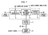
- FIG. 7 A switching amplifier comprising a conventional power amplifier is shown in FIG. 7.
- This conventional example relates to a switching amplifier for audio.
- This switching amplifier is provided with an audio power amplifier 1 and a power supply 6, the audio power amplifier 1 being provided with a ⁇ modulator 2 for ⁇ modulating an audio signal.
- the construction is such that an output pulse signal from this ⁇ modulator 2 is supplied to a power switching element 3 in the amplifier, and then output via an output filter 4 in the amplifier.
- the power supply 6 is connected to this power switching element 3 in the amplifier, the construction being such that the power supply 6 receives a clock signal, performs pulse width modulation in synchronization with this clock signal, supplies this pulse width modulated signal to a power switching element in the power supply, and supplies required power to the power switching element 3 in the amplifier via an output filter in the power supply.
- This conventional example of a switching amplifier operates as follows. Firstly, a signal such as an audio signal or the like is input to the ⁇ modulator 2, and a sampling clock is input to this ⁇ modulator 2 at the same time. The input signal is ⁇ modulated by the ⁇ modulator 2, and the output pulse signal thereof is input to the power switching element 3 in the amplifier. In addition, a different clock signal from the sampling clock signal is input to the power supply 6, pulse width modulation is performed in synchronization with this clock signal, and the pulse width modulated output pulse signal is input to the power switching element in the power supply. The output of the power switching element in the power supply is output through an output filter 7 in the power supply, and supplies power to the power switching element 3 in the amplifier.
- the present invention takes the above problems into consideration, with an object of providing a new switching amplifier that reduces the switching noise of a power supply, in particular to achieve an improvement in quality.
- the timing of switching noise in the power amplifier and the power supply is almost the same, and even if noise from the power supply is mixed in, it is possible to use a common noise filter in the power amplifier. Furthermore, a noise filter for power supply is unnecessary, and it is also not necessary to have a smoothing circuit equipped with a comparatively large-sized capacitor and choke coil in the power supply output, so that it is possible to simplify the output filter of the power supply. Moreover, simplification of the power supply output filter enables the switching amplifier to be miniaturized and cost reduced.
- the present invention has the following construction in order to solve the above problems.
- a switching amplifier comprises: a switching power amplifier which has a modulator which modulates an analog signal or a multi bit digital signal into a two-level signal, and supplies an output pulse signal from the modulator to a power switching element; and a ⁇ power supply which has a ⁇ modulating device which ⁇ modulates an analog signal or a multi bit digital signal, and supplies a pulse signal for power supply control output from the ⁇ modulating device to a power switching element in the power supply, wherein an output pulse signal of the modulator in the power amplifier is supplied to the ⁇ power supply, and the output pulse signal is input as an operating clock to the ⁇ power supply, and the output power of the ⁇ power supply is supplied to the power switching element in the power amplifier.
- a switching amplifier comprises: a power amplifier having at least a pair of power switching elements in the output stage thereof, which modulates an input signal comprising an analog signal or a multi bit digital signal into a two-level signal, and obtains an output signal power amplified by controlling the conductivity of the power switching elements complimentarily based on the two-level signal; and a switching power supply which generates a required power supply voltage to be supplied to the power switching elements by switching in synchronization with the two-level signal.
- a switching amplifier according to a third aspect of the present invention is that, in a switching amplifier according to the second aspect of the present invention, an operation timing between the switching power supply and the power amplifier is set such that noise accompanying the switching operation of the switching power supply occurs within a predetermined period during which the power switching elements installed in the output stage are both off.
- a switching amplifier according to a fourth aspect of the present invention is that, in a switching amplifier according to the second or the third aspects of the present invention, the switching power supply comprises a ⁇ power supply, which receives the two-level signal as an operating clock signal.
- a switching amplifier is one where, in the switching amplifier according to the fourth aspect of the present invention, the switching power supply comprises: a voltage converting section having a switching element inserted in a current path of an external power supply, and which converts the voltage of the external power supply into the required power supply voltage by switching this switching element; and a switching control section which ⁇ modulates the power supply voltage converted by the voltage converting section, and controls switching of switching elements constituting the voltage converting section based on a signal obtained by this ⁇ modulation.
- the switching operation of the switching power supply is synchronized with a two-level signal which controls the conduction of a pair of power switching elements on the power amplifier side, and is synchronized with the switching of these pair of power switching elements. Consequently it is possible to match the timing of noise occurring accompanying the switching operation of the switching power supply with the timing of switching the pair of power switching elements in the output stage, so that the occurrence of switching noise on the output signal appears to be reduced virtually. Furthermore, by adjusting the timing such that noise accompanying the switching operation of the switching power supply occurs within a predetermined period during which the pair of power switching elements is off, noise accompanying the switching operation of the switching power supply does not appear on the output signal via the pair of power switching elements. As a result, it is possible to miniaturize a filter for suppressing noise accompanying the switching operation of a switching power supply or power switching elements.
- FIG. 1 shows one embodiment according to the present invention.
- FIG. 2 shows an example of the principal part of this embodiment.
- the embodiment shown in FIG. 1 is a switching amplifier in which an audio power amplifier 1 is installed.
- the audio power amplifier 1 is provided with a ⁇ modulator 2 which ⁇ modulates an audio signal, and its construction is such that an output pulse signal from this ⁇ modulator 2 is supplied to a power switching element 3 in the amplifier, and then output through an output filter 4 in the amplifier.
- the present embodiment is provided with a ⁇ power supply 5.
- An output pulse signal from the ⁇ modulator 2 in the audio power amplifier 1 is supplied to this ⁇ power supply 5, and this output pulse signal is input as an operating clock to the ⁇ power supply 5 to generate the required power, and the power is supplied to the power switching element 3 in the amplifier.
- FIG. 2 A specific structure of a ⁇ power supply according to the present embodiment is shown in FIG. 2.
- This ⁇ power supply 5 is provided with a ⁇ modulator 16, and supplies an output pulse signal from this ⁇ modulator 16 to a power switching element 11 in the power supply. Furthermore, it is provided with a smoothing circuit 12, and the output side of this smoothing circuit 12 is connected to the ⁇ modulator 16 which ⁇ modulates an analog signal or a multi bit digital signal, via an error amplifier 14 which amplifies the differential voltage between the voltage output to a load 13 and a reference voltage 15, and the signal of the differential voltage between the voltage output to the load and the reference voltage 15 is amplified by the error amplifier 14, and the amplified signal is input to the ⁇ modulator 16.
- the reference voltage 15 is the target value for the output voltage VO, and the switching operation is performed such that the output voltage VO is stabilized to the reference voltage 15.
- the output voltage VO may be lowered by a resistance type potential divider, input to the error amplifier 14, and the reference voltage 15 may be set as the target value of the voltage obtained by this resistance type potential divider. In this case, the output voltage VO is stabilized to the required voltage by the voltage obtained by the resistance type potential divider being stabilized to the reference voltage 15.
- the ⁇ power supply 5 as shown in FIG. 2 is just one embodiment, and any construction may be used for the ⁇ power supply 5 according to the present invention provided it uses a ⁇ modulation technique.
- it is not limited to a ⁇ power supply, and any switching power supply may be used provided it can use a clock whose frequency is not fixed as an operating clock, that is, a variable frequency clock signal.
- any power supply may be used provided it can synchronize its turning on and off with a clock.
- FIG. 3 shows the principal part of the structure shown in FIG. 1.
- the ⁇ modulator 2 comprises a modulation circuit 2A and a drive circuit 2B.
- the modulation circuit 2A modulates an input signal SI and converts it to a pulsed signal SS (two-level signal).
- the pulse width of this pulsed signal SS is influenced by the input signal SI.
- the drive circuit 2B drives a power switching element 3 complementarily, based on the pulsed signal SS, and outputs driving signals SP and SN for that purpose.
- This modulator 2 operates with a power supply of about 5V, for example.
- a positive power supply 5A and a negative power supply 5B are switching power supplies for generating the required high power supply voltages (for example, several tens volt) to be supplied to power MOS transistors 3A and 3B, and constitute the ⁇ power supply 5 as shown in FIG. 1 described above.
- the construction is such that the positive power supply 5A and the negative power supply 5B receives the pulsed signal SS as an operating clock, and generate a positive high power supply voltage VP and a negative high power supply voltage VN by switching in synchronization with this pulsed signal SS.
- the ⁇ power supply 5 comprises a stabilizing capacitor C1, the switching element 11 inserted in the current path of an external power supply (not shown in the figure), a free wheel diode D, and the smoothing circuit 12 (inductor L and capacitor C2).
- This functions as a voltage converting section (symbol omitted) for converting an input voltage V1 from the external power supply into a required output voltage VO.
- the ⁇ power supply 5 contains the error amplifier 14, the ⁇ modulator 16, and a gate driver circuit 17, in addition to the voltage converting section described above. These constitute a switching control section (symbol omitted) for controlling switching of the switching element 11.
- the example shown in FIG. 2 is constructed as a step down power supply. However, it is not limited to this, and for example this may be constructed as a step up power supply.
- the switching element 11 is connected in series with a step up coil connected to the external power supply.
- the construction is such that the switching element 11 is inserted in the current path of the external power supply similarly to the step down type.
- FIG. 4 shows the structure of the ⁇ modulator 16 described above.
- the ⁇ modulator 16 comprises a subtractor 20, an integrator 21, a comparator 22 and a D type flip-flop (D-FF) 23.
- the subtractor 20 subtracts a switching control signal SG from an output signal VG from the error amplifier 14 described above, and the integrator 21 integrates the output signal from the subtractor 20.
- the comparator 22 quantizes the output signal from the integrator 21 to a two-level signal based on a reference voltage 24, and the output signal from the integrator 21 is applied to the noninverting input terminal thereof, and the reference voltage 15 is applied to the inverting input terminal thereof.
- the reference voltage 24 regulates the operation of the ⁇ modulation, and specifically, it provides a judgment level for when the output signal ( ⁇ signal) from the integrator 21 is made binary. This reference voltage 24 is set appropriately according to the required characteristics of ⁇ modulation.
- the D type flip-flop 23 latches the output signal from the comparator 22, using the pulsed signal SS output from the modulation circuit 2A described above as a clock signal.
- the power switching element 3 comprises the pair of n channel type power MOS output transistors 3A and 3B, whose current paths are connected in series between the positive power supply 5A and the negative power supply 5B.
- the drain of the power MOS transistor 3A is connected to the positive power supply 5A, and the driving signal SP described above is applied to its gate.
- the source of the power MOS transistor 3B is connected to the negative power supply 5B, and the driving signal SN described above is applied to its gate.
- the source of the power MOS transistor 3A and the drain of the power MOS transistor 3B are connected to each other to form the output section of the power switching element 3, which is connected to the input section of the output filter 4 in the subsequent stage.
- the pair of n channel type power MOS transistors 3A and 3B, constituting the power switching element 3, form a so-called half bridge.
- this is not limiting, and a plurality of power MOS transistor pairs may be used to form a so-called full bridge.
- a switching amplifier constructed as above operates as follows. Firstly, an audio signal is input to the ⁇ modulator 2 as an input signal SI, and also a sampling clock SC is input to the ⁇ modulator 2. The audio signal is ⁇ modulated by the ⁇ modulator 2, and the output pulse signal is input to the power switching element 3 in the amplifier. Similarly, the output pulse signal of the ⁇ modulator 2 for audio signal is input to the ⁇ power supply 5 as a clock signal.
- an output signal from the ⁇ modulator 2 has two conditions, ON and OFF, and since this change can only occur at either a rising or falling edge of the clock input to the ⁇ modulator 16 in the ⁇ power supply 5, switching noise generated from the power switching element 3 in the amplifier connected to the output of the ⁇ modulator also occurs at the same time.
- an output pulse signal from the ⁇ modulator in the amplifier is input to the power switching element 3 in the amplifier, and is input to the ⁇ power supply 5 as a clock signal at the same time, so that the ON and OFF changes of the power switching element 11 in the power supply occur at only either a rising or falling edge of the output pulse from the ⁇ modulator 2 in the amplifier.
- the timing of switching noise from the audio power amplifier 1 and the ⁇ power supply 5 is almost the same.
- the audio power amplifier 1 modulates the input signal SI comprising an analog signal or a multi bit digital signal to a pulsed signal (two-level signal) SS. Then, a power amplified output signal SO is obtained by controlling the conductivity of the pair of power MOS transistors installed in the output stage complementarily based on the pulsed signal SS.
- the modulator 2 as shown in FIG. 3 ⁇ modulates the input signal SI based on the sampling clock SC, and outputs the pulsed signal SS.
- This pulsed signal SS is applied to the drive circuit 2B in the subsequent stage, and is also applied to the positive power supply 5A and the negative power supply 5B constituting the ⁇ power supply 5.
- the ⁇ modulator 16 shown in FIG. 2 and FIG. 4 generates a switching control signal SG using the pulsed signal SS as an operating clock signal, and applies this switching control signal SG to the gate of the switching element 11 as shown in FIG. 2.
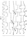
- the high power supply 5A performs switching operations, and maintains a substantially steady high power supply voltage VP as shown in FIG. 5.
- the waveforms of the high power supply voltage VP show only a ripple component.
- the negative power supply 5B performs switching operations based on the pulsed signal SS, and generates a substantially steady negative high power supply voltage VN.
- the D type flip-flop 23 in the structure of the ⁇ modulator 16 shown in FIG. 4 latches the output signal from the comparator 22 at the rising edge of the pulsed signal SS, and outputs this as a switching control signal SG.
- the switching control signal SG changes at the rising edge of the pulsed signal SS as shown in FIG 5. Therefore, switching noise SNZ caused by the switching operation based on the switching control signal SG is superimposed onto the high power supply voltages VP and VN.
- the drive circuit 2B outputs the driving signals SP and SN in response to the pulsed signal SS output from the ⁇ modulation circuit 2A, drives the power MOS transistors 3A and 3B complimentarily, and outputs the output signal SO via the output filter 4.
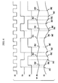
- the operating timing between the ⁇ power supply 5 and the audio power amplifier 1 based on the pulsed signal SS is set such that the switching noise SNZ that is superimposed onto the high power supply voltages VP and VN is generated within the period (within a predetermined period) of the dead time DT.
- the timing does not need to be adjusted, and the switching noise SNZ is generated within the period of the dead time DT.
- a timing setting device for adjusting this timing may be provided as required.
- a delay circuit may be used as this device.
- the pulsed signal SS is divided into one to be supplied to the positive power supplies 5A and 5B, and one to be supplied to the drive circuit 2B, and one of these divided pulse signals may be delayed from the other by an appropriate amount.
- the switching noise SNZ caused by the power supply 6 is superimposed onto the output signal SO in addition to the output noise ONZ, with a result that noise on the output signal SO increases compared with the case where the ⁇ power supply 5 is used.
- the aforementioned embodiment makes it possible to reduce noise occurring on the output signal SO effectively without increasing the size of the output filter 4, which is installed in the audio power amplifier 1, and the filter (not shown in the figure) for suppressing the noise on the power supply side. As a result, it is possible to amplify the power of signals with high quality.
- the present embodiment describes a switching amplifier in which an audio power amplifier 1 is installed. However, it may also be used for a switching amplifier in which any other power amplifier for amplifying an analog signal or a multi bit digital signal is installed.
- the present embodiment describes a case where the audio power amplifier 1 uses ⁇ modulation as a modulating technique.
- the same effect may be obtained using any other modulating technique provided it is a method for modulating an input signal to two states ON and OFF.
- pulse width modulation may be used.
- the timing may be set such that these noises interfere intentionally.
- the noise on the output signal SO is offset each other.
- the description uses a step down chopper type as the ⁇ power supply 5.
- a step up type may be used for the ⁇ power supply 5.
- the timing of switching noise occurring in the power amplifier and the power supply is almost the same, so that there is an effect that even if noise from the power supply is mixed in, it is possible to use a common noise filter in the power amplifier. Furthermore, a noise filter for power supply is unnecessary, and it is also not necessary to have a smoothing circuit equipped with a comparatively large-sized capacitor and choke coil in the power supply output, so that there is an effect that the output filter of the power supply can be simplified. Moreover, there is an effect that simplification of the power supply output filter enables the switching amplifier to be miniaturized and cost reduced.
Landscapes
- Engineering & Computer Science (AREA)
- Power Engineering (AREA)
- Amplifiers (AREA)
Applications Claiming Priority (3)
| Application Number | Priority Date | Filing Date | Title |
|---|---|---|---|
| JP2001267305 | 2001-09-04 | ||
| JP2001267305 | 2001-09-04 | ||
| PCT/JP2002/008979 WO2003021769A1 (fr) | 2001-09-04 | 2002-09-04 | Appareil d'amplification de commutation |
Publications (2)
| Publication Number | Publication Date |
|---|---|
| EP1427101A1 true EP1427101A1 (fr) | 2004-06-09 |
| EP1427101A4 EP1427101A4 (fr) | 2006-05-17 |
Family
ID=19093449
Family Applications (1)
| Application Number | Title | Priority Date | Filing Date |
|---|---|---|---|
| EP02765412A Withdrawn EP1427101A4 (fr) | 2001-09-04 | 2002-09-04 | Appareil d'amplification de commutation |
Country Status (6)
| Country | Link |
|---|---|
| US (1) | US6831509B2 (fr) |
| EP (1) | EP1427101A4 (fr) |
| JP (1) | JP4017596B2 (fr) |
| KR (1) | KR100494757B1 (fr) |
| CA (1) | CA2431297C (fr) |
| WO (1) | WO2003021769A1 (fr) |
Cited By (3)
| Publication number | Priority date | Publication date | Assignee | Title |
|---|---|---|---|---|
| EP1614214A1 (fr) * | 2003-04-07 | 2006-01-11 | Philips Intellectual Property & Standards GmbH | Amplificateur numerique |
| FR2966994A1 (fr) * | 2010-11-02 | 2012-05-04 | Cddic | Amplificateur audio class-d pwm combine avec un elevateur de tension et avec controle de dissipation. |
| US8995691B2 (en) | 2008-07-14 | 2015-03-31 | Audera Acoustics Inc. | Audio amplifier |
Families Citing this family (8)
| Publication number | Priority date | Publication date | Assignee | Title |
|---|---|---|---|---|
| US7126416B2 (en) * | 2004-11-17 | 2006-10-24 | Princeton Technology Corporation | Pulse amplitude modulation (PAM) method and circuit for improving the performance of a D-class audio amplifier |
| JP2008047945A (ja) * | 2005-03-28 | 2008-02-28 | Nec Saitama Ltd | アンプ装置 |
| JP4574466B2 (ja) * | 2005-06-29 | 2010-11-04 | シャープ株式会社 | 音声再生装置 |
| FR2890258B1 (fr) * | 2005-08-30 | 2007-10-12 | Thales Sa | Dispositif et procede pour amplifier des signaux rf impulsionnels |
| US20090261902A1 (en) * | 2008-04-17 | 2009-10-22 | Freescale Semiconductor, Inc. | Asynchronous Error Correction Circuit for Switching Amplifier |
| JP5337120B2 (ja) * | 2010-09-13 | 2013-11-06 | パナソニック株式会社 | D級増幅器及び無線通信装置 |
| CN115421021B (zh) * | 2022-08-17 | 2026-03-03 | 成都华微电子科技股份有限公司 | 集成电路和集成电路电源开关同步噪声测试方法 |
| CN115567007B (zh) * | 2022-12-05 | 2023-03-10 | 四川湖山电器股份有限公司 | 一种功率放大器直流工作点跟踪电路 |
Family Cites Families (10)
| Publication number | Priority date | Publication date | Assignee | Title |
|---|---|---|---|---|
| US4016501A (en) * | 1975-12-29 | 1977-04-05 | Motorola, Inc. | Switching amplifier system |
| JPS55166314A (en) | 1979-06-14 | 1980-12-25 | Sony Corp | Pulse duration modulating/amplifying circuit |
| US5075634A (en) * | 1990-11-23 | 1991-12-24 | Blade Technologies Inc. | Composite bridge amplifier |
| JPH05219743A (ja) | 1992-02-04 | 1993-08-27 | Shindengen Electric Mfg Co Ltd | 降圧チヨッパ回路の力率改善方法 |
| WO1994011799A1 (fr) * | 1992-11-10 | 1994-05-26 | Motorola, Inc. | Regulateur de commutation et systeme amplificateur |
| US6373335B1 (en) * | 1997-09-18 | 2002-04-16 | Robert W Carver | Integrated audio amplifier |
| JP3348019B2 (ja) * | 1998-07-06 | 2002-11-20 | シャープ株式会社 | パルス波増幅装置 |
| JP3445179B2 (ja) | 1998-12-28 | 2003-09-08 | シャープ株式会社 | Δς変調を用いるスイッチング増幅器 |
| US6717392B2 (en) * | 2000-05-30 | 2004-04-06 | Rádiodetection Limited | Signal generator |
| JP2002158549A (ja) * | 2000-11-17 | 2002-05-31 | Sony Corp | デジタルパワーアンプ装置 |
-
2002
- 2002-09-04 JP JP2003525985A patent/JP4017596B2/ja not_active Expired - Fee Related
- 2002-09-04 EP EP02765412A patent/EP1427101A4/fr not_active Withdrawn
- 2002-09-04 WO PCT/JP2002/008979 patent/WO2003021769A1/fr not_active Ceased
- 2002-09-04 KR KR10-2003-7006094A patent/KR100494757B1/ko not_active Expired - Fee Related
- 2002-09-04 US US10/450,039 patent/US6831509B2/en not_active Expired - Fee Related
- 2002-09-04 CA CA002431297A patent/CA2431297C/fr not_active Expired - Fee Related
Cited By (3)
| Publication number | Priority date | Publication date | Assignee | Title |
|---|---|---|---|---|
| EP1614214A1 (fr) * | 2003-04-07 | 2006-01-11 | Philips Intellectual Property & Standards GmbH | Amplificateur numerique |
| US8995691B2 (en) | 2008-07-14 | 2015-03-31 | Audera Acoustics Inc. | Audio amplifier |
| FR2966994A1 (fr) * | 2010-11-02 | 2012-05-04 | Cddic | Amplificateur audio class-d pwm combine avec un elevateur de tension et avec controle de dissipation. |
Also Published As
| Publication number | Publication date |
|---|---|
| US20040124914A1 (en) | 2004-07-01 |
| KR20030063370A (ko) | 2003-07-28 |
| US6831509B2 (en) | 2004-12-14 |
| CA2431297C (fr) | 2006-02-14 |
| CA2431297A1 (fr) | 2003-03-13 |
| JPWO2003021769A1 (ja) | 2004-12-24 |
| WO2003021769A1 (fr) | 2003-03-13 |
| JP4017596B2 (ja) | 2007-12-05 |
| EP1427101A4 (fr) | 2006-05-17 |
| KR100494757B1 (ko) | 2005-06-14 |
Similar Documents
| Publication | Publication Date | Title |
|---|---|---|
| US11962275B2 (en) | Amplification systems and methods with distortion reductions | |
| US6489841B2 (en) | Class D audio amplifier | |
| US7843260B2 (en) | Method and apparatus for high performance class D audio amplifiers | |
| US20120001659A1 (en) | Voltage-to-Current Converter with Feedback | |
| US6831509B2 (en) | Switching amplification apparatus | |
| US7456685B2 (en) | Class D audio amplifier with PWM and feedback | |
| US6922100B2 (en) | Method and apparatus for switching amplification having variable sample point and variable order correction | |
| US6586991B2 (en) | Digital power amplifier | |
| KR20010034031A (ko) | 증폭기에 의해 생성된 dc 오프셋 및 노이즈를감소시키는 수단을 포함하는 회로 | |
| US20050196177A1 (en) | Laser driver circuit with signal transition enhancement | |
| US20080238543A1 (en) | Digital Amplifier with Analogue Error Correction Circuit | |
| US7777562B2 (en) | Distortion suppression circuit for digital class-D audio amplifier | |
| US7518442B1 (en) | Circuit and method for suppressing switching and supply-related errors in a PWM power stage by instantaneous per-pulse feedback | |
| US6420930B1 (en) | Class D audio amplifier | |
| JP2004194334A (ja) | Pdmd級増幅器の線形化 | |
| US7183818B2 (en) | Triangular wave generating circuit adapted to class-D amplifier | |
| JPH07254823A (ja) | デルタシグマ変調増幅器 | |
| US11205999B2 (en) | Amplifier with signal dependent mode operation | |
| US6717538B2 (en) | DA converter and data reproducing apparatus | |
| US7315209B2 (en) | Power amplifier apparatus and DC component removing method | |
| JP4380933B2 (ja) | スイッチング信号制御回路 | |
| EP4014323B1 (fr) | Émetteur à modulation polaire avec commande de mode de produit à large bande | |
| JP3776738B2 (ja) | スイッチング信号生成器 | |
| JP2006101022A (ja) | デジタルアンプ |
Legal Events
| Date | Code | Title | Description |
|---|---|---|---|
| PUAI | Public reference made under article 153(3) epc to a published international application that has entered the european phase |
Free format text: ORIGINAL CODE: 0009012 |
|
| 17P | Request for examination filed |
Effective date: 20030626 |
|
| AK | Designated contracting states |
Kind code of ref document: A1 Designated state(s): AT BE BG CH CY CZ DE DK EE ES FI FR GB GR IE IT LI LU MC NL PT SE SK TR |
|
| AX | Request for extension of the european patent |
Extension state: AL LT LV MK RO SI |
|
| RIN1 | Information on inventor provided before grant (corrected) |
Inventor name: MITAMURA, ATSUSHI,C/O SHINDENGEN ELECTRIC |
|
| A4 | Supplementary search report drawn up and despatched |
Effective date: 20060404 |
|
| RIC1 | Information provided on ipc code assigned before grant |
Ipc: H03F 1/02 20060101ALI20060329BHEP Ipc: H03F 3/217 20060101AFI20030320BHEP |
|
| 17Q | First examination report despatched |
Effective date: 20080417 |
|
| STAA | Information on the status of an ep patent application or granted ep patent |
Free format text: STATUS: THE APPLICATION IS DEEMED TO BE WITHDRAWN |
|
| 18D | Application deemed to be withdrawn |
Effective date: 20080828 |