EP1429191A1 - Méthode de détermination de paramètres pour projection lithographique - Google Patents
Méthode de détermination de paramètres pour projection lithographique Download PDFInfo
- Publication number
- EP1429191A1 EP1429191A1 EP03257723A EP03257723A EP1429191A1 EP 1429191 A1 EP1429191 A1 EP 1429191A1 EP 03257723 A EP03257723 A EP 03257723A EP 03257723 A EP03257723 A EP 03257723A EP 1429191 A1 EP1429191 A1 EP 1429191A1
- Authority
- EP
- European Patent Office
- Prior art keywords
- source
- elements
- substrate
- radiation
- pattern
- Prior art date
- Legal status (The legal status is an assumption and is not a legal conclusion. Google has not performed a legal analysis and makes no representation as to the accuracy of the status listed.)
- Granted
Links
- 238000000034 method Methods 0.000 title claims abstract description 86
- 238000009826 distribution Methods 0.000 claims abstract description 27
- 230000005855 radiation Effects 0.000 claims description 64
- 239000000758 substrate Substances 0.000 claims description 50
- 238000000059 patterning Methods 0.000 claims description 30
- 230000003287 optical effect Effects 0.000 claims description 27
- 238000012937 correction Methods 0.000 claims description 19
- 238000004519 manufacturing process Methods 0.000 claims description 7
- 239000013598 vector Substances 0.000 claims description 7
- 238000004590 computer program Methods 0.000 claims description 6
- 239000000463 material Substances 0.000 claims description 6
- 238000013500 data storage Methods 0.000 claims description 4
- 210000001747 pupil Anatomy 0.000 description 18
- 238000005286 illumination Methods 0.000 description 15
- 239000010410 layer Substances 0.000 description 11
- 238000004364 calculation method Methods 0.000 description 9
- 230000006870 function Effects 0.000 description 6
- 230000000694 effects Effects 0.000 description 4
- 238000003384 imaging method Methods 0.000 description 4
- 238000005457 optimization Methods 0.000 description 4
- XUIMIQQOPSSXEZ-UHFFFAOYSA-N Silicon Chemical compound [Si] XUIMIQQOPSSXEZ-UHFFFAOYSA-N 0.000 description 3
- 238000001459 lithography Methods 0.000 description 3
- 229910052710 silicon Inorganic materials 0.000 description 3
- 239000010703 silicon Substances 0.000 description 3
- 238000003491 array Methods 0.000 description 2
- 238000005094 computer simulation Methods 0.000 description 2
- 238000010276 construction Methods 0.000 description 2
- 238000013461 design Methods 0.000 description 2
- 238000010894 electron beam technology Methods 0.000 description 2
- 239000011159 matrix material Substances 0.000 description 2
- 230000010363 phase shift Effects 0.000 description 2
- 239000011295 pitch Substances 0.000 description 2
- 238000012545 processing Methods 0.000 description 2
- 238000004458 analytical method Methods 0.000 description 1
- 230000002238 attenuated effect Effects 0.000 description 1
- 230000005540 biological transmission Effects 0.000 description 1
- 239000011248 coating agent Substances 0.000 description 1
- 238000000576 coating method Methods 0.000 description 1
- 239000002131 composite material Substances 0.000 description 1
- 230000001143 conditioned effect Effects 0.000 description 1
- 230000003750 conditioning effect Effects 0.000 description 1
- 230000003247 decreasing effect Effects 0.000 description 1
- 230000001419 dependent effect Effects 0.000 description 1
- 238000001514 detection method Methods 0.000 description 1
- 238000011161 development Methods 0.000 description 1
- 230000009977 dual effect Effects 0.000 description 1
- 230000005684 electric field Effects 0.000 description 1
- 230000005670 electromagnetic radiation Effects 0.000 description 1
- 238000005530 etching Methods 0.000 description 1
- 238000001914 filtration Methods 0.000 description 1
- 230000014509 gene expression Effects 0.000 description 1
- 230000005484 gravity Effects 0.000 description 1
- 238000007689 inspection Methods 0.000 description 1
- 238000005468 ion implantation Methods 0.000 description 1
- 238000010884 ion-beam technique Methods 0.000 description 1
- 239000002346 layers by function Substances 0.000 description 1
- 239000004973 liquid crystal related substance Substances 0.000 description 1
- 230000005381 magnetic domain Effects 0.000 description 1
- 238000005259 measurement Methods 0.000 description 1
- 230000015654 memory Effects 0.000 description 1
- QSHDDOUJBYECFT-UHFFFAOYSA-N mercury Chemical compound [Hg] QSHDDOUJBYECFT-UHFFFAOYSA-N 0.000 description 1
- 229910052753 mercury Inorganic materials 0.000 description 1
- 238000001465 metallisation Methods 0.000 description 1
- 230000003647 oxidation Effects 0.000 description 1
- 238000007254 oxidation reaction Methods 0.000 description 1
- 239000002245 particle Substances 0.000 description 1
- 230000000737 periodic effect Effects 0.000 description 1
- 230000036314 physical performance Effects 0.000 description 1
- 238000005498 polishing Methods 0.000 description 1
- 230000037452 priming Effects 0.000 description 1
- 239000004065 semiconductor Substances 0.000 description 1
- 238000007493 shaping process Methods 0.000 description 1
- 238000003860 storage Methods 0.000 description 1
- 239000010409 thin film Substances 0.000 description 1
- 238000012795 verification Methods 0.000 description 1
Images



Classifications
-
- G—PHYSICS
- G03—PHOTOGRAPHY; CINEMATOGRAPHY; ANALOGOUS TECHNIQUES USING WAVES OTHER THAN OPTICAL WAVES; ELECTROGRAPHY; HOLOGRAPHY
- G03F—PHOTOMECHANICAL PRODUCTION OF TEXTURED OR PATTERNED SURFACES, e.g. FOR PRINTING, FOR PROCESSING OF SEMICONDUCTOR DEVICES; MATERIALS THEREFOR; ORIGINALS THEREFOR; APPARATUS SPECIALLY ADAPTED THEREFOR
- G03F7/00—Photomechanical, e.g. photolithographic, production of textured or patterned surfaces, e.g. printing surfaces; Materials therefor, e.g. comprising photoresists; Apparatus specially adapted therefor
- G03F7/70—Microphotolithographic exposure; Apparatus therefor
- G03F7/70058—Mask illumination systems
- G03F7/70125—Use of illumination settings tailored to particular mask patterns
-
- G—PHYSICS
- G03—PHOTOGRAPHY; CINEMATOGRAPHY; ANALOGOUS TECHNIQUES USING WAVES OTHER THAN OPTICAL WAVES; ELECTROGRAPHY; HOLOGRAPHY
- G03F—PHOTOMECHANICAL PRODUCTION OF TEXTURED OR PATTERNED SURFACES, e.g. FOR PRINTING, FOR PROCESSING OF SEMICONDUCTOR DEVICES; MATERIALS THEREFOR; ORIGINALS THEREFOR; APPARATUS SPECIALLY ADAPTED THEREFOR
- G03F7/00—Photomechanical, e.g. photolithographic, production of textured or patterned surfaces, e.g. printing surfaces; Materials therefor, e.g. comprising photoresists; Apparatus specially adapted therefor
- G03F7/70—Microphotolithographic exposure; Apparatus therefor
- G03F7/70425—Imaging strategies, e.g. for increasing throughput or resolution, printing product fields larger than the image field or compensating lithography- or non-lithography errors, e.g. proximity correction, mix-and-match, stitching or double patterning
- G03F7/70433—Layout for increasing efficiency or for compensating imaging errors, e.g. layout of exposure fields for reducing focus errors; Use of mask features for increasing efficiency or for compensating imaging errors
- G03F7/70441—Optical proximity correction [OPC]
Definitions
- the present invention relates to the determination of parameters, in particular radiation source intensity distribution, optical proximity correction rules and process windows for lithographic projection using a lithographic projection apparatus, more particularly for a lithographic projection apparatus comprising:
- patterning means as here employed should be broadly interpreted as referring to means that can be used to endow an incoming radiation beam with a patterned cross-section, corresponding to a pattern that is to be created in a target portion of the substrate; the term “light valve” can also be used in this context.
- the said pattern will correspond to a particular functional layer in a device being created in the target portion, such as an integrated circuit or other device (see below). Examples of such patterning means include:
- Lithographic projection apparatus can be used, for example, in the manufacture of integrated circuits (ICs).
- the patterning means may generate a circuit pattern corresponding to an individual layer of the IC, and this pattern can be imaged onto a target portion (e.g. comprising one or more dies) on a substrate (silicon wafer) that has been coated with a layer of radiation-sensitive material (resist).
- a target portion e.g. comprising one or more dies
- a substrate silicon wafer
- a layer of radiation-sensitive material resist
- a single wafer will contain a whole network of adjacent target portions that are successively irradiated via the projection system, one at a time.
- employing patterning by a mask on a mask table a distinction can be made between two different types of machine.
- each target portion is irradiated by exposing the entire mask pattern onto the target portion in one go; such an apparatus is commonly referred to as a wafer stepper.
- each target portion is irradiated by progressively scanning the mask pattern under the projection beam in a given reference direction (the "scanning" direction) while synchronously scanning the substrate table parallel or anti-parallel to this direction; since, in general, the projection system will have a magnification factor M (generally ⁇ 1), the speed V at which the substrate table is scanned will be a factor M times that at which the mask table is scanned.
- M magnification factor
- a pattern (e.g. in a mask) is imaged onto a substrate that is at least partially covered by a layer of radiation-sensitive material (resist).
- the substrate Prior to this imaging step, the substrate may undergo various procedures, such as priming, resist coating and a soft bake. After exposure, the substrate may be subjected to other procedures, such as a post-exposure bake (PEB), development, a hard bake and measurement/inspection of the imaged features.
- PEB post-exposure bake
- This array of procedures is used as a basis to pattern an individual layer of a device, e.g. an IC.
- Such a patterned layer may then undergo various processes such as etching, ion-implantation (doping), metallization, oxidation, chemo-mechanical polishing, etc., all intended to finish off an individual layer. If several layers are required, then the whole procedure, or a variant thereof, will have to be repeated for each new layer. Eventually, an array of devices will be present on the substrate (wafer). These devices are then separated from one another by a technique such as dicing or sawing, whence the individual devices can be mounted on a carrier, connected to pins, etc.
- the projection system may hereinafter be referred to as the "lens"; however, this term should be broadly interpreted as encompassing various types of projection system, including refractive optics, reflective optics, and catadioptric systems, for example.
- the radiation system may also include components operating according to any of these design types for directing, shaping or controlling the projection beam of radiation, and such components may also be referred to below, collectively or singularly, as a "lens".
- the lithographic apparatus may be of a type having two or more substrate tables (and/or two or more mask tables). In such "multiple stage” devices the additional tables may be used in parallel, or preparatory steps may be carried out on one or more tables while one or more other tables are being used for exposures. Dual stage lithographic apparatus are described, for example, in US 5,969,441 and WO 98/40791, incorporated herein by reference.
- optical proximity effect In lithography there is a problem known as the optical proximity effect. This is caused by the inherent difference in diffraction pattern for isolated features as compared to dense features. Dense features may include nested patterns and closely spaced periodic features. The optical proximity effect leads to a difference in critical dimension (CD) when dense and more isolated lines are printed at the same time. The lines are different when printed even though they are identical on the mask.
- CD critical dimension
- the optical proximity effect also depends on the illumination setting used. Originally, so-called conventional illumination modes have been used which have a disc-like intensity distribution of the illumination radiation at the pupil of the projection lens. However, with the trend to imaging smaller features, off-axis illumination modes have become standard in order to improve the process window, i.e. exposure and/or focus latitude, for small features. However, the optical proximity effect can become worse for off-axis illumination modes, such as annular illumination.
- OPC optical proximity correction
- OPC optical proximity correction
- the radiation source is divided into blocks and the system is modeled as being equivalent to a point source at each block which is either on or off. For each source point in turn the resulting intensity at selected points on the substrate is calculated. An optimization routine is then used to calculate the optimum source distribution comprising a plurality of illumination source blocks so as to minimize the difference between the calculated intensity at the substrate and the ideal intensity at the substrate for best printing of the pattern. Another technique is to calculate the difference between the actual intensity and ideal intensity for every block of the radiation source and place them in rank-order. The overall illumination intensity distribution is obtained by accepting the source blocks in rank order until the illumination reaches a threshold. Further details of these techniques can be obtained from US 6,045,976, incorporated herein by reference.
- a method for determining a projection beam source intensity distribution and optical proximity correction rules for a patterning means for use with a lithographic projection apparatus comprising:
- a further aspect of the present invention provides a computer system comprising a data processor and data storage means, the data processor being adapted to process data in accordance with an executable program stored in the data storage means, wherein the executable program is adapted to execute the above method.
- the invention also provides a computer program comprising program code means for executing on a computer the above method, and a computer program product carrying the computer program.
- Another aspect of the invention provides a method of manufacturing a device using a lithographic projection apparatus comprising:
- the terms "radiation” and “beam” are used to encompass all types of electromagnetic radiation, including ultraviolet radiation (e.g. with a wavelength of 365, 248, 193, 157 or 126 nm) and EUV (extreme ultra-violet radiation, e.g. having a wavelength in the range 5-20 nm), as well as particle beams, such as ion beams or electron beams.
- ultraviolet radiation e.g. with a wavelength of 365, 248, 193, 157 or 126 nm
- EUV extreme ultra-violet radiation, e.g. having a wavelength in the range 5-20 nm
- particle beams such as ion beams or electron beams.
- Figure 1 schematically depicts a lithographic projection apparatus according to a particular embodiment of the invention.
- the apparatus comprises:
- the source LA (e . g . a Hg lamp, excimer laser, a discharge source, laser produced plasma LPP, an undulator provided around a path of an electron beam in a storage ring or synchrotron) produces a beam of radiation.
- This beam is fed into an illumination system (illuminator) IL, either directly or after having traversed conditioning means, such as a beam expander Ex, for example.
- the illuminator IL may comprise adjusting means AM for setting the outer and/or inner radial extent (commonly referred to as ⁇ -outer and ⁇ -inner, respectively) of the intensity distribution in the beam.
- it will generally comprise various other components, such as an integrator IN and a condenser CO.
- the beam PB impinging on the mask MA has a desired uniformity and intensity distribution in its cross-section.
- the source LA may be within the housing of the lithographic projection apparatus (as is often the case when the source LA is a mercury lamp, for example), but that it may also be remote from the lithographic projection apparatus, the radiation beam which it produces being led into the apparatus (e.g. with the aid of suitable directing mirrors); this latter scenario is often the case when the source LA is an excimer laser.
- the current invention and claims encompass both of these scenarios.
- the beam PB subsequently intercepts the mask MA, which is held on a mask table MT. Having been selectively reflected by the mask MA, the beam PB passes through the lens PL, which focuses the beam PB onto a target portion C of the substrate W. With the aid of the second positioning means (and interferometric measuring means IF), the substrate table WT can be moved accurately, e.g. so as to position different target portions C in the path of the beam PB. Similarly, the first positioning means can be used to accurately position the mask MA with respect to the path of the beam PB, e.g. after mechanical retrieval of the mask MA from a mask library, or during a scan.
- the mask table MT may just be connected to a short stroke actuator, or may be fixed.
- the depicted apparatus can be used in two different modes:
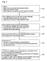
- Figure 2 shows a flow chart of a method embodying the invention for use with the lithographic projection apparatus of Figure 1.
- step S10 for a pattern which it is desired to image on to a substrate, a plurality of features are selected and their allowed size margins, i.e. critical dimensions, are specified.
- Figure 3 shows schematically a portion of a pattern to be imaged and three features 11, 12, 13 indicated by the rings are examples of selected features.
- step S10 Further initialization is done in step S10 to define the allowed optical proximity correction (OPC) range, i.e. the limits to the amount of biasing (e.g. widening or lengthening) of features that can be permitted and limits on the assist feature sizes, and to select the minimum overlapping process window OPW threshold that is acceptable.
- OPC optical proximity correction
- the lower limit that describes what OPW is still acceptable can be defined in terms of: 1) maximum focus latitude of the OPW; 2) maximum exposure latitude of the OPW; 3) a function of 1) and 2) for example the product of the two; 4) the area of the OPW; or 5) a combination of the above factors, for example combined using logical operators such as AND and OR.
- steps S20 to S40 do not have to be performed on an actual lithographic projection apparatus as depicted in Figure 1, but are, of course, performed using a computer model that simulates the physical apparatus and so the pattern, illumination system, projection lens and so on are represented as digital data. Thus references to these items should, of course, be read to include corresponding virtual items in a computer model.
- the radiation source is notionally divided into elements.
- radiation source or equivalently “projection beam source” used herein could refer to the actual source that generates the radiation, such as a laser, or could, for example, refer to a portion in the radiation path which acts as a virtual or "secondary” source, such as an integrator or other means which has conditioned the radiation, and which effectively acts as a "source” for subsequent items in the beam path.
- the radiation source comprises the beam at a pupil in the illumination system.
- the pupil is typically circular and is represented schematically by the circle 14 in Figure 4(a).
- the complete radiation source has an intensity distribution as a function of position in the pupil 14 that corresponds to the angular intensity distribution of radiation incident on the mask.
- the radiation source is divided into a plurality of elements, each element corresponding to a region or pixel of the source.
- Each source element may be either "on” or “off'.
- the overall source can be considered to be the sum of the elements that are "on”.
- each source element can be approximated by a point source, such as indicated by the cross 15 in Figure 4(a).
- the calculation described below for step S20 is performed in turn for every elemental region into which the source has been divided, i.e. every point on the grid in Figure 4(a), to span the complete pupil.
- the source at the pupil have certain symmetry for reasons of telecentricity, i.e. preferably the center of gravity of the distribution should lie at the center of the pupil. Consequently, according to another embodiment shown in Figure 4(b), it suffices to construct a symmetrical source by dividing the pupil 14 into two halves with each source element for the calculation comprising two sub-elements 15, 16, one in each half, and diametrically opposite each other with respect to the optical axis (center of the pupil).
- a single source "element" for the purposes of the calculation can be composed of a number of sub-elements 15, 16.
- the amount of calculation is reduced to one half by considering sources in only one half (indicated by the grid on the left half of Figure 4(b)) and using the symmetry to produce the sources in the other half.
- the pupil is divided in quadrants, and each source element comprises four sub-elements obtained by reflecting the point source 15 in the first quadrant about the vertical and horizontal axes to produce the sources indicated by the crosses at 16, 17 and 18 in the other three quadrants.
- each source element comprises four sub-elements obtained by reflecting the point source 15 in the first quadrant about the vertical and horizontal axes to produce the sources indicated by the crosses at 16, 17 and 18 in the other three quadrants.
- this can work just as well because of the fact that the positive and negative orders of the diffraction pattern are generally identical, and will reduce the amount of computation to approximately one quarter.
- the source elements lie on a rectangular grid, but this is purely one example of constructing the source elements; any other suitable division may be used, depending on the circumstances, such as a hexagonal grid or point sources arranged according to polar coordinates.
- the source pupil 14 could also be divided into six or another number of regions other than two or four. The exact location of the grid areas within the pupil can be purely arbitrary.
- a further improved embodiment for creating composite source elements i.e. source elements composed of multiple point sources, will be described with reference to Figure 5.
- the left half of the pupil is divided into a grid of N points as shown in the upper left portion of Figure 5. One of these points is chosen together with the corresponding symmetric point in the right half of the pupil, as shown by the two crosses.
- the bottom half of the pupil is divided into a grid of M points ( M can be the same as N ), and a further pair of symmetric source points is chosen, shown by the two small squares in the upper center illustration of Figure 5.
- the final chosen source element used for the calculation of step S20 is the sum of the two source pairs from steps (i) and (ii), i.e.
- the source element comprises four sub-elements depicted by two crosses and two squares in the upper right portion of Figure 5. Steps (ii) and (iii) are then iterated M times going through all M “top/bottom” source point pairs, keeping the source pair from step (i) the same; then returning to step (i) the "left/right” source pair is incremented to the next pair of points, followed by iteration of steps (ii) and (iii) another M times. This is repeated until all N "left/right” source pairs have been evaluated with all M "top/bottom” source pairs, giving a total of M * N source elements, schematically depicted in the right hand column of Figure 5. The analysis of OPC and OPW described below is performed for each of these M * N source elements for each selected pattern feature.
- the division of the source pupil into left/right and top/bottom halves by horizontal and vertical dividing lines can be otherwise than depicted, e.g. rotated by an arbitrary angle and/or not necessarily orthogonal to each other.
- the only criterion is that the directions of the dividing lines are not identical. This embodiment has been described with respect to dividing the pupil into halves (as in Figure 4(b)), but could equally be done with no division as in Figure 4(a) or division into quadrants as in Figure 4(c), or any other division.
- step S20 for each source element (e.g. composed of sub-elements 15, 16, 17 and 18 of Figure 4(c)) the process window for each selected feature is calculated, for example as described in "Inside Prolith” by Chris A Mack 1997 (ISBN 0-9650922-0-8), particularly chapter 10.
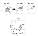
- Figure 6(a) illustrates schematically, for one source element, the process windows 21, 22 and 23 for the selected features 11, 12 and 13.
- the process windows defme the ranges of dose and focus (i.e. exposure latitude EL and focus latitude (depth of focus DOF)) which will result in acceptable printing of the feature within the defined size margins.
- the OPC rules are then determined which optimize the overlapping of the process windows. This can be straightforward e.g. by applying bias to the structures with the larger spacing, in order to effectively decrease the local dose. As the local dose is effectively decreased, then the process window for that feature is pushed up so that a higher dose is required to expose that feature.
- Figure 6(c) shows the resulting overlapping process window OPW representing the available process window in which the selected features can all be successfully printed for the given source element and by applying the calculated OPC rules. This is repeated such that for each source element a set of OPC rules is determined and an optimized OPW is obtained.
- Figure 7 is a schematic plot of the results of step S20. Each cross represents a plot of the OPC and OPW for a particular source element. Figure 7 is purely a schematic 2D-plot to assist understanding of the invention. In practice, each set of OPC rules can be represented mathematically as a multidimensional vector and the crosses lie in a multidimensional vector space. As explained previously, the OPW can be characterized by many parameters, for example exposure latitude, focus latitude, window area or combinations thereof. The OPW criteria can be combined into one value which is plotted vertically in Figure 7.
- the quantity plotted vertically could represent the function: [Maximum DOF of the OPW] with a threshold on [Maximum DOF of the OPW] AND a threshold on [Maximum Exposure Latitude of the OPW].
- this function is written: MaxDOF & (MaxDOF > F & MaxEL > E ). This will plot the MaxDOF for those source points where the MaxDOF is larger than a chosen value F and simultaneously MaxEL is larger than a chosen value E . This is merely an example. Many other combinations can be thought of.
- the radiation source elements must be evaluated and those selected which are to form the intensity distribution of the optimized source.
- the selected source elements must have an OPW which meets the minimum threshold specified in step S10.
- the threshold is indicated by the dashed horizontal line in Figure 7.
- the threshold might be, for example, that the maximum depth of focus (DOF) is greater than 0.3 ⁇ m and the maximum exposure latitude (EL) is greater than 7%.
- DOE maximum depth of focus
- EL maximum exposure latitude
- the threshold uses more than one parameter.
- the source elements corresponding to the crosses below that line can be eliminated. Effectively this could be done using the function described above for plotting the points in Figure 7.
- the source elements must have a substantially common set of OPC rules such that there is consistency when designing the patterning means, such as the mask.
- this is done by identifying a region in the plot of Figure 7 that has a high density of crosses with a similar OPC. A suitable region is indicated by the dashed ellipse 30 in Figure 7.
- this method step looks for a region in the multidimensional OPC vector space that has a high density of points. Points are then selected starting in the high density region with the primary criterion that there must be enough source elements such that the overall illumination is adequately bright; for example, for practical purposes at least 10% of the area of the source pupil must be illuminated.
- Figure 7 is simply an illustration to assist understanding of the invention. The calculation can be done by a processor manipulating the relevant data.
- the final set of OPC rules is determined in step S35.
- the set of OPC rules is effectively given by the OPC vector that approximates to the common OPC vector for these selected source elements.
- the final set of OPC rules is determined using the entire optimized source, comprising the sum of the selected source elements, rather than using the source elements separately.
- the OPC rules are determined using known software routines, as explained previously, that optimize the OPW.
- the results of the optimization method are output.
- the results comprise data representing the group of selected radiation source elements and the set of OPC rules.
- the process window for the group of selected source elements can also be output, but this is not essential.
- the group of selected radiation source elements are those which correspond to the crosses within the region 30.
- the optimized radiation source intensity distribution is given by the sum of these elements.
- the process window information can assist with the correct exposure of the pattern using the OPC rules and the optimized source, but this information is not essential for setting up a lithography apparatus such a stepper or scanner.
- the apparatus for performing the method of steps S10 to S40 does not have to be part of the lithographic projection apparatus of Figure 1 and can be a conventional computer system that has access to the data representing the pattern to be imaged and the physical performance of the protection apparatus.
- the apparatus can be a system dedicated for use with the lithographic projection apparatus.
- the computer system for performing the calculation of the optimal or near-optimal radiation source and OPC may comprise software for performing a method embodying the invention stored in a data store and executed by a processor.
- the data output on the group of selected radiation source elements, which comprise the desired intensity distribution of the source can be used to construct an actual radiation source having that intensity distribution. This may be done by including one or more beam-defining members in the illuminator IL of the projection apparatus, for example comprising optical means such as a grey filter or spatial filter, or any suitable refractive, reflective, diffractive or filtering means for defining the intensity distribution.
- the data on the set of optimized OPC rules can be applied to the desired pattern to design a patterning means, such as a mask, for use in exposing a substrate.
- the method can include the step of imaging the pattern onto a substrate using the radiation source and patterning means above and exposing the image within the process window obtained in step S40.
Landscapes
- Physics & Mathematics (AREA)
- General Physics & Mathematics (AREA)
- Exposure And Positioning Against Photoresist Photosensitive Materials (AREA)
Priority Applications (1)
| Application Number | Priority Date | Filing Date | Title |
|---|---|---|---|
| EP20030257723 EP1429191B1 (fr) | 2002-12-09 | 2003-12-09 | Méthode de détermination de paramètres pour projection lithographique |
Applications Claiming Priority (3)
| Application Number | Priority Date | Filing Date | Title |
|---|---|---|---|
| EP02258468 | 2002-12-09 | ||
| EP02258468 | 2002-12-09 | ||
| EP20030257723 EP1429191B1 (fr) | 2002-12-09 | 2003-12-09 | Méthode de détermination de paramètres pour projection lithographique |
Publications (2)
| Publication Number | Publication Date |
|---|---|
| EP1429191A1 true EP1429191A1 (fr) | 2004-06-16 |
| EP1429191B1 EP1429191B1 (fr) | 2008-11-26 |
Family
ID=32327859
Family Applications (1)
| Application Number | Title | Priority Date | Filing Date |
|---|---|---|---|
| EP20030257723 Expired - Lifetime EP1429191B1 (fr) | 2002-12-09 | 2003-12-09 | Méthode de détermination de paramètres pour projection lithographique |
Country Status (1)
| Country | Link |
|---|---|
| EP (1) | EP1429191B1 (fr) |
Citations (4)
| Publication number | Priority date | Publication date | Assignee | Title |
|---|---|---|---|---|
| US6045976A (en) * | 1992-06-02 | 2000-04-04 | Fujitsu, Limited | Optical exposure method |
| US6320648B1 (en) * | 1998-10-12 | 2001-11-20 | Steven R. J. Brueck | Method and apparatus for improving pattern fidelity in diffraction-limited imaging |
| EP1237046A2 (fr) * | 2001-02-28 | 2002-09-04 | ASML Masktools B.V. | Méthode pour l identification des regions d interaction extrème, méthodes pour créer des motifs de masque et production de masques, méthodes pour la fabrication de dispositifs et programmes d'ordinateur |
| EP1239331A2 (fr) * | 2001-02-23 | 2002-09-11 | ASML Netherlands B.V. | Optimisation d illumination de motifs spécifiques |
-
2003
- 2003-12-09 EP EP20030257723 patent/EP1429191B1/fr not_active Expired - Lifetime
Patent Citations (4)
| Publication number | Priority date | Publication date | Assignee | Title |
|---|---|---|---|---|
| US6045976A (en) * | 1992-06-02 | 2000-04-04 | Fujitsu, Limited | Optical exposure method |
| US6320648B1 (en) * | 1998-10-12 | 2001-11-20 | Steven R. J. Brueck | Method and apparatus for improving pattern fidelity in diffraction-limited imaging |
| EP1239331A2 (fr) * | 2001-02-23 | 2002-09-11 | ASML Netherlands B.V. | Optimisation d illumination de motifs spécifiques |
| EP1237046A2 (fr) * | 2001-02-28 | 2002-09-04 | ASML Masktools B.V. | Méthode pour l identification des regions d interaction extrème, méthodes pour créer des motifs de masque et production de masques, méthodes pour la fabrication de dispositifs et programmes d'ordinateur |
Also Published As
| Publication number | Publication date |
|---|---|
| EP1429191B1 (fr) | 2008-11-26 |
Similar Documents
| Publication | Publication Date | Title |
|---|---|---|
| US7026082B2 (en) | Method for determining parameters for lithographic projection, a computer system and computer program therefor, a method of manufacturing a device and a device manufactured thereby | |
| US6792591B2 (en) | Method of identifying an extreme interaction pitch region, methods of designing mask patterns and manufacturing masks, device manufacturing methods and computer programs | |
| US6839125B2 (en) | Method for optimizing an illumination source using full resist simulation and process window response metric | |
| KR100457839B1 (ko) | 규정된 래더바를 서브-해상도 어시스트피처로 활용하는광근접성교정방법 | |
| US7548302B2 (en) | Lithographic apparatus and device manufacturing method | |
| JP3867904B2 (ja) | 特定のマスク・パターンのための照明の最適化 | |
| KR100459090B1 (ko) | 극단상호작용피치영역을 확인하는 방법, 마스크패턴을설계하고 마스크를 제조하는 방법, 디바이스제조방법 및컴퓨터프로그램 | |
| US6887625B2 (en) | Assist features for use in lithographic projection | |
| US7180576B2 (en) | Exposure with intensity balancing to mimic complex illuminator shape | |
| JP4974972B2 (ja) | 照明源最適化によってレンズ収差補償を行う方法および装置 | |
| EP1286218A2 (fr) | Formation de motifs lithographiques utilisant un masque avec déphaseurs attenués de transmission élevée et plusieurs expositions de cohérence optimalisée | |
| US6875545B2 (en) | Method of removing assist features utilized to improve process latitude | |
| US7317506B2 (en) | Variable illumination source | |
| EP1467252A1 (fr) | Méthode de fabrication d'un dispositif et ensemble de réticules destiné à l'application de cette méthode | |
| EP1480080A1 (fr) | Appareil lithographique et méthode de fabrication d'un dispositif | |
| EP1429191B1 (fr) | Méthode de détermination de paramètres pour projection lithographique | |
| US7735052B2 (en) | Method of identifying an extreme interaction pitch region, methods of designing mask patterns and manufacturing masks, device manufacturing methods and computer programs | |
| JP4639120B2 (ja) | マスク・パターンの光転送を最適化するための方法、リソグラフィ投影装置、および機械可読媒体 | |
| EP1467256A1 (fr) | Méthode de fabrication d'un dispositif et ensemble de réticules destiné à l'application de cette méthode | |
| EP1434097A2 (fr) | Appareil lithographique et procédé pour la production d'un dispositif |
Legal Events
| Date | Code | Title | Description |
|---|---|---|---|
| PUAI | Public reference made under article 153(3) epc to a published international application that has entered the european phase |
Free format text: ORIGINAL CODE: 0009012 |
|
| AK | Designated contracting states |
Kind code of ref document: A1 Designated state(s): AT BE BG CH CY CZ DE DK EE ES FI FR GB GR HU IE IT LI LU MC NL PT RO SE SI SK TR |
|
| AX | Request for extension of the european patent |
Extension state: AL LT LV MK |
|
| RAP1 | Party data changed (applicant data changed or rights of an application transferred) |
Owner name: ASML NETHERLANDS B.V. |
|
| 17P | Request for examination filed |
Effective date: 20041214 |
|
| AKX | Designation fees paid |
Designated state(s): DE FR GB IT NL |
|
| 17Q | First examination report despatched |
Effective date: 20050318 |
|
| GRAP | Despatch of communication of intention to grant a patent |
Free format text: ORIGINAL CODE: EPIDOSNIGR1 |
|
| GRAS | Grant fee paid |
Free format text: ORIGINAL CODE: EPIDOSNIGR3 |
|
| GRAA | (expected) grant |
Free format text: ORIGINAL CODE: 0009210 |
|
| AK | Designated contracting states |
Kind code of ref document: B1 Designated state(s): DE FR GB IT NL |
|
| REG | Reference to a national code |
Ref country code: GB Ref legal event code: FG4D |
|
| REF | Corresponds to: |
Ref document number: 60324884 Country of ref document: DE Date of ref document: 20090108 Kind code of ref document: P |
|
| NLV1 | Nl: lapsed or annulled due to failure to fulfill the requirements of art. 29p and 29m of the patents act | ||
| PG25 | Lapsed in a contracting state [announced via postgrant information from national office to epo] |
Ref country code: NL Free format text: LAPSE BECAUSE OF FAILURE TO SUBMIT A TRANSLATION OF THE DESCRIPTION OR TO PAY THE FEE WITHIN THE PRESCRIBED TIME-LIMIT Effective date: 20081126 |
|
| PLBE | No opposition filed within time limit |
Free format text: ORIGINAL CODE: 0009261 |
|
| STAA | Information on the status of an ep patent application or granted ep patent |
Free format text: STATUS: NO OPPOSITION FILED WITHIN TIME LIMIT |
|
| GBPC | Gb: european patent ceased through non-payment of renewal fee |
Effective date: 20090226 |
|
| PG25 | Lapsed in a contracting state [announced via postgrant information from national office to epo] |
Ref country code: DE Free format text: LAPSE BECAUSE OF NON-PAYMENT OF DUE FEES Effective date: 20090701 |
|
| 26N | No opposition filed |
Effective date: 20090827 |
|
| PG25 | Lapsed in a contracting state [announced via postgrant information from national office to epo] |
Ref country code: FR Free format text: LAPSE BECAUSE OF NON-PAYMENT OF DUE FEES Effective date: 20090126 Ref country code: GB Free format text: LAPSE BECAUSE OF NON-PAYMENT OF DUE FEES Effective date: 20090226 |
|
| REG | Reference to a national code |
Ref country code: FR Ref legal event code: ST Effective date: 20111216 |
|
| PG25 | Lapsed in a contracting state [announced via postgrant information from national office to epo] |
Ref country code: IT Free format text: LAPSE BECAUSE OF FAILURE TO SUBMIT A TRANSLATION OF THE DESCRIPTION OR TO PAY THE FEE WITHIN THE PRESCRIBED TIME-LIMIT Effective date: 20081126 |