EP1237046A2 - Méthode pour l identification des regions d interaction extrème, méthodes pour créer des motifs de masque et production de masques, méthodes pour la fabrication de dispositifs et programmes d'ordinateur - Google Patents
Méthode pour l identification des regions d interaction extrème, méthodes pour créer des motifs de masque et production de masques, méthodes pour la fabrication de dispositifs et programmes d'ordinateur Download PDFInfo
- Publication number
- EP1237046A2 EP1237046A2 EP02251365A EP02251365A EP1237046A2 EP 1237046 A2 EP1237046 A2 EP 1237046A2 EP 02251365 A EP02251365 A EP 02251365A EP 02251365 A EP02251365 A EP 02251365A EP 1237046 A2 EP1237046 A2 EP 1237046A2
- Authority
- EP
- European Patent Office
- Prior art keywords
- illumination
- pitch
- identifying
- angles
- extreme interaction
- Prior art date
- Legal status (The legal status is an assumption and is not a legal conclusion. Google has not performed a legal analysis and makes no representation as to the accuracy of the status listed.)
- Granted
Links
Images




Classifications
-
- G—PHYSICS
- G03—PHOTOGRAPHY; CINEMATOGRAPHY; ANALOGOUS TECHNIQUES USING WAVES OTHER THAN OPTICAL WAVES; ELECTROGRAPHY; HOLOGRAPHY
- G03F—PHOTOMECHANICAL PRODUCTION OF TEXTURED OR PATTERNED SURFACES, e.g. FOR PRINTING, FOR PROCESSING OF SEMICONDUCTOR DEVICES; MATERIALS THEREFOR; ORIGINALS THEREFOR; APPARATUS SPECIALLY ADAPTED THEREFOR
- G03F7/00—Photomechanical, e.g. photolithographic, production of textured or patterned surfaces, e.g. printing surfaces; Materials therefor, e.g. comprising photoresists; Apparatus specially adapted therefor
- G03F7/70—Microphotolithographic exposure; Apparatus therefor
- G03F7/70483—Information management; Active and passive control; Testing; Wafer monitoring, e.g. pattern monitoring
- G03F7/70491—Information management, e.g. software; Active and passive control, e.g. details of controlling exposure processes or exposure tool monitoring processes
- G03F7/705—Modelling or simulating from physical phenomena up to complete wafer processes or whole workflow in wafer productions
-
- H—ELECTRICITY
- H10—SEMICONDUCTOR DEVICES; ELECTRIC SOLID-STATE DEVICES NOT OTHERWISE PROVIDED FOR
- H10P—GENERIC PROCESSES OR APPARATUS FOR THE MANUFACTURE OR TREATMENT OF DEVICES COVERED BY CLASS H10
- H10P76/00—Manufacture or treatment of masks on semiconductor bodies, e.g. by lithography or photolithography
-
- G—PHYSICS
- G03—PHOTOGRAPHY; CINEMATOGRAPHY; ANALOGOUS TECHNIQUES USING WAVES OTHER THAN OPTICAL WAVES; ELECTROGRAPHY; HOLOGRAPHY
- G03F—PHOTOMECHANICAL PRODUCTION OF TEXTURED OR PATTERNED SURFACES, e.g. FOR PRINTING, FOR PROCESSING OF SEMICONDUCTOR DEVICES; MATERIALS THEREFOR; ORIGINALS THEREFOR; APPARATUS SPECIALLY ADAPTED THEREFOR
- G03F7/00—Photomechanical, e.g. photolithographic, production of textured or patterned surfaces, e.g. printing surfaces; Materials therefor, e.g. comprising photoresists; Apparatus specially adapted therefor
- G03F7/70—Microphotolithographic exposure; Apparatus therefor
- G03F7/70058—Mask illumination systems
- G03F7/70125—Use of illumination settings tailored to particular mask patterns
-
- G—PHYSICS
- G03—PHOTOGRAPHY; CINEMATOGRAPHY; ANALOGOUS TECHNIQUES USING WAVES OTHER THAN OPTICAL WAVES; ELECTROGRAPHY; HOLOGRAPHY
- G03F—PHOTOMECHANICAL PRODUCTION OF TEXTURED OR PATTERNED SURFACES, e.g. FOR PRINTING, FOR PROCESSING OF SEMICONDUCTOR DEVICES; MATERIALS THEREFOR; ORIGINALS THEREFOR; APPARATUS SPECIALLY ADAPTED THEREFOR
- G03F7/00—Photomechanical, e.g. photolithographic, production of textured or patterned surfaces, e.g. printing surfaces; Materials therefor, e.g. comprising photoresists; Apparatus specially adapted therefor
- G03F7/70—Microphotolithographic exposure; Apparatus therefor
- G03F7/70425—Imaging strategies, e.g. for increasing throughput or resolution, printing product fields larger than the image field or compensating lithography- or non-lithography errors, e.g. proximity correction, mix-and-match, stitching or double patterning
- G03F7/70433—Layout for increasing efficiency or for compensating imaging errors, e.g. layout of exposure fields for reducing focus errors; Use of mask features for increasing efficiency or for compensating imaging errors
-
- G—PHYSICS
- G03—PHOTOGRAPHY; CINEMATOGRAPHY; ANALOGOUS TECHNIQUES USING WAVES OTHER THAN OPTICAL WAVES; ELECTROGRAPHY; HOLOGRAPHY
- G03F—PHOTOMECHANICAL PRODUCTION OF TEXTURED OR PATTERNED SURFACES, e.g. FOR PRINTING, FOR PROCESSING OF SEMICONDUCTOR DEVICES; MATERIALS THEREFOR; ORIGINALS THEREFOR; APPARATUS SPECIALLY ADAPTED THEREFOR
- G03F7/00—Photomechanical, e.g. photolithographic, production of textured or patterned surfaces, e.g. printing surfaces; Materials therefor, e.g. comprising photoresists; Apparatus specially adapted therefor
- G03F7/70—Microphotolithographic exposure; Apparatus therefor
- G03F7/70425—Imaging strategies, e.g. for increasing throughput or resolution, printing product fields larger than the image field or compensating lithography- or non-lithography errors, e.g. proximity correction, mix-and-match, stitching or double patterning
- G03F7/70433—Layout for increasing efficiency or for compensating imaging errors, e.g. layout of exposure fields for reducing focus errors; Use of mask features for increasing efficiency or for compensating imaging errors
- G03F7/70441—Optical proximity correction [OPC]
Definitions
- the present invention relates to photolithography and more particularly to optical proximity correction methods used during the development of photolithography masks for use in lithographic apparatus comprising:
- patterning means as here employed should be broadly interpreted as referring to means that can be used to endow an incoming radiation beam with a patterned cross-section, corresponding to a pattern that is to be created in a target portion of the substrate; the term “light valve” can also be used in this context.
- the said pattern will correspond to a particular functional layer in a device being created in the target portion, such as an integrated circuit or other device (see below). Examples of such patterning means include:
- Lithographic projection apparatus can be used, for example, in the manufacture of integrated circuits (ICs).
- the patterning means may generate a circuit pattern corresponding to an individual layer of the IC, and this pattern can be imaged onto a target portion (e.g. comprising one or more dies) on a substrate (silicon wafer) that has been coated with a layer of radiation-sensitive material (resist).
- a target portion e.g. comprising one or more dies
- a substrate silicon wafer
- a layer of radiation-sensitive material resist
- a single wafer will contain a whole network of adjacent target portions that are successively irradiated via the projection system, one at a time.
- employing patterning by a mask on a mask table a distinction can be made between two different types of machine.
- each target portion is irradiated by exposing the entire mask pattern onto the target portion in one go; such an apparatus is commonly referred to as a wafer stepper.
- each target portion is irradiated by progressively scanning the mask pattern under the projection beam in a given reference direction (the "scanning" direction) while synchronously scanning the substrate table parallel or anti-parallel to this direction; since, in general, the projection system will have a magnification factor M (generally ⁇ 1), the speed V at which the substrate table is scanned will be a factor M times that at which the mask table is scanned.
- M magnification factor
- a pattern (e.g. in a mask) is imaged onto a substrate that is at least partially covered by a layer of radiation-sensitive material (resist).
- the substrate Prior to this imaging step, the substrate may undergo various procedures, such as priming, resist coating and a soft bake. After exposure, the substrate may be subjected to other procedures, such as a post-exposure bake (PEB), development, a hard bake and measurement/inspection of the imaged features.
- PEB post-exposure bake
- This array of procedures is used as a basis to pattern an individual layer of a device, e.g. an IC.
- Such a patterned layer may then undergo various processes such as etching, ion-implantation (doping), metallization, oxidation, chemo-mechanical polishing, etc., all intended to finish off an individual layer. If several layers are required, then the whole procedure, or a variant thereof, will have to be repeated for each new layer. Eventually, an array of devices will be present on the substrate (wafer). These devices are then separated from one another by a technique such as dicing or sawing, whence the individual devices can be mounted on a carrier, connected to pins, etc.
- the projection system may hereinafter be referred to as the "lens"; however, this term should be broadly interpreted as encompassing various types of projection system, including refractive optics, reflective optics, and catadioptric systems, for example.
- the radiation system may also include components operating according to any of these design types for directing, shaping or controlling the projection beam of radiation, and such components may also be referred to below, collectively or singularly, as a "lens".
- the lithographic apparatus may be of a type having two or more substrate tables (and/or two or more mask tables). In such "multiple stage” devices the additional tables may be used in parallel, or preparatory steps may be carried out on one or more tables while one or more other tables are being used for exposures. Dual stage lithographic apparatus are described, for example, in US 5,969,441 and WO 98/40791, incorporated herein by reference.
- a "critical dimension” of a circuit is defined as the smallest width of a feature or the smallest space between two features.
- OPE optical proximity effect
- Optical proximity effects are a well known characteristic of optical projection exposure tools. More specifically, proximity effects occur when very closely spaced circuit patterns are lithographically transferred to a resist layer on a wafer. The light waves of the closely spaced circuit features interact, thereby distorting the final transferred pattern features. In other words, diffraction causes adjacent features to interact with each other in such a way as to produce pattern dependent variations. The magnitude of the OPE on a given feature depends on the feature's placement on the mask with respect to other features.
- OPE optical proximity correction
- An object of the invention is to provide a method for optimizing mask patterns for use with various different illumination schemes.
- the present invention provides a method and technique for identifying and eliminating forbidden pitch regions, which degrade the overall printing performance, so as to allow for an improvement of the CDs and process latitude obtainable utilizing currently known photolithography tools and techniques.
- the "forbidden pitch" regions are regions in which both the critical dimension of the feature and the process latitude of the feature are negatively affected.
- the inventors of the present invention have noted that some optical phenomenon have become more prominent.
- the inventors have noticed a forbidden pitch phenomena. More specifically, there are pitch ranges within which the process latitude of a "densely located" main feature, especially the exposure latitude, is worse than that of an isolated feature of the same size. This important observation indicates that the existence of the neighboring feature is not always beneficial for main feature printing, which is in contradiction to what is commonly conceived, prior to the discovery by the present inventors. Indeed, the present inventors believe that the forbidden pitch phenomenon has become a limiting factor in advanced photolithography. As such, suppressing the forbidden pitch phenomenon will be necessary to further improve the CDs and process latitude obtainable utilizing currently known semiconductor device manufacturing tools and techniques.
- the present invention relates to a method of identifying undesirable pitches between features when designing an integrated circuit (or other device) to be formed on a substrate by use of a lithographic exposure tool.
- the method comprises the steps of (a) identifying extreme interaction pitch regions by determining illumination intensity levels for a given illumination angle over a range of pitches; and (b) identifying the undesirable pitches for each extreme interaction pitch region identified in step (a) by determining illumination intensities for a given extreme interaction pitch region over a range of illumination angles.
- the variation of the critical dimension as well as the process latitude of a main feature is a direct consequence of light field interference between the main feature and the neighboring features.
- the main feature critical dimension and process latitude can be improved by constructive light field interference, or degraded by destructive light field interference.
- the phase of the field produced by the neighboring features can be shown to be dependent on the pitch as well as the illumination angle.
- the forbidden pitch lies in the location where the field produced by the neighboring features interferes with the field of the main feature destructively.
- the present invention provides a method for identifying the forbidden pitch regions (i.e., locations) for any feature size and any illumination condition.
- the present invention provides a method for performing illumination design in order to suppress the forbidden pitch phenomena, thereby suppressing the negative effects associated therewith.
- the present invention provides for a method for utilizing scattering bar placement in conjunction with the suppression of the forbidden pitch phenomena to further minimize optical proximity effects and optimize overall printing performance.
- the present invention provides significant advantages over the prior art. Most importantly, the present invention provides for identifying and eliminating forbidden pitch regions, which degrade the overall printing performance, thereby allowing for an improvement of the CDs and process latitude obtainable utilizing currently known photolithography tools and techniques.
- the "mask pattern” may be embodied in a mask but may also be applied using another type of patterning means, examples of which are mentioned above.
- the term “mask pattern” is used herein for convenience but should not be construed as requiring the presence of a mask, unless the context otherwise requires.
- the terms "radiation” and “beam” are used to encompass all types of electromagnetic radiation, including ultraviolet radiation (e.g. with a wavelength of 365, 248, 193, 157 or 126 nm) and EUV (extreme ultra-violet radiation, e.g. having a wavelength in the range 5-20 nm), as well as particle beams, such as ion beams or electron beams.
- ultraviolet radiation e.g. with a wavelength of 365, 248, 193, 157 or 126 nm
- EUV extreme ultra-violet radiation, e.g. having a wavelength in the range 5-20 nm
- particle beams such as ion beams or electron beams.
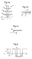
- Fig. 1a illustrates an exemplary imaging system.
- Figs. 1b and 1c illustrate the transformation of an on-axis image point at the exit pupil into a corresponding point in the two-dimensional frequency plane.
- Fig. 2 represents an exemplary mask pattern to be printed on a wafer.
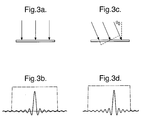
- Figs. 3a-3d illustrate exemplary results of both on-axis illumination and off-axis illumination.
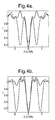
- Figs. 4a and 4b illustrate an exemplary interaction between side features and the main feature at two different pitches under a specific illumination angle.
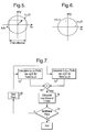
- Fig. 5 is a graph representing two-dimensional illumination.
- Fig. 6 is a graph representing the conjugated illumination scheme required for vertical and horizontal feature performance balance.
- Fig. 7 illustrates a flow chart detailing the process of defining/identifying the forbidden pitch regions.
- Fig. 8 is a plot resulting from the process of Fig. 7, which illustrates the extreme interaction pitch regions.
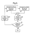
- Fig. 9 illustrates a flow chart detailing the process of generating the illumination map for a given pitch.
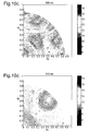
- Figs. 10a-10c show the illumination maps corresponding to the extreme interaction pitch regions of 480 nm, 560 nm, 635 nm illustrated in Fig. 8, respectively.
- Fig. 10d illustrates the illumination map corresponding to the pitch of 310 nm.
- Fig. 11 illustrates an illumination design that improves the exposure latitude at the 480 nm pitch region while preserving strong constructive structural interactions at other pitch regions.
- Fig. 12 is a graph illustrating a comparison of the log-slope values associated with annular, quadrupole and the modified quadrupole illumination.
- Fig. 13 shows the extreme interaction edge-to-edge placement positions of the scattering bars around an isolated main line.
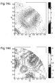
- Figs. 14a-d are illumination maps for scattering bars having varying separation from a main feature.
- the forbidden pitch phenomenon is a direct consequence of optical interactions between neighboring features. More specifically, the field phase of the neighboring feature relative to that of the main feature depends on the illumination angle and the separation distance between the features. For a given illumination angle, there are pitch ranges within which the field phase produced by the neighboring feature is substantially 180° out of phase relative to the field phase of the main feature, thereby resulting in destructive interference. Such destructive interference reduces the image contrast of the main feature, and as a result, causes a loss of exposure latitude. It is these pitch ranges, which cause destructive interference, that are referred to as the forbidden pitch ranges, and that are identified and eliminated by the methods of the present invention.
- the forbidden pitch regions are mapped out or identified utilizing an illumination map.
- a corresponding illumination map is obtained, which shows its favorable illumination regions and its unfavorable illumination regions.
- the illumination maps can be eliminated.
- the neighboring feature size is changed to the scattering bar size, similar constructive and destructive interference regions can be located and their corresponding illumination maps can also be obtained. Based on these illumination maps, the present invention also allows for optimal scattering bar placement to be determined for a given illumination condition.
- the imaging process can be viewed as a double diffraction process under coherent illumination.
- the lens acts as the Fourier transform device that converts the geometrical information of the object (i.e., the reticle) into the spatial frequency information of the object in the frequency domain.
- the spatial frequency information of the object i.e., frequency components and their amplitudes
- the object can be viewed as purely geometrical and scalar diffraction theory is applicable.
- the foregoing assumptions are currently considered valid for a reduction projection optical imaging system with a binary chrome reticle.
- the electric field at the exit pupil is related to the transmission function of the object through the Fourier transformation.
- 4X or 5X reduction projection systems are utilized in practical photolithography systems, the following discussion utilizes a 1X system in order to simplify the analysis.
- the 1X optical imaging system avoids the complexity of information conversion from entrance pupil to exit pupil that is required for a 4X or 5X reduction optical imaging system, namely, the spatial frequency conversion, the field magnitude conversion and polarization tracking. It is noted, however, that the present invention is equally applicable to other systems, including a 4X or 5X reduction optical imaging system, or any other applicable system.
- Fig. 1a illustrates an exemplary imaging system 10 helpful for describing the operation of the present invention.
- the imaging system 10 comprises a monochromatic light source 12, a condenser 14, a reticle 16, and a projection lens 18.
- the imaging process generates an exit pupil 20 and an image plane 22.
- the illumination scheme is Köhler illumination so that uniform illumination is achieved.
- an adjustable aperture stop is placed at the back focal plane of the projection lens 18, then the back focal plane becomes the exit pupil because there are no optical elements between the back focal plane and the image plane.
- each geometrical point at the exit pupil 20 corresponds to a pair of angular coordinates ( ⁇ , ⁇ ), which can be transformed into a corresponding point in the two-dimensional frequency plane through the following transformation, described by equation (1) and shown in Figs. 1b and 1c.
- k x sin ⁇ cos ⁇
- k y sin ⁇ sin ⁇
- f ( x o ) 1 - (1 + ⁇ ) ⁇ rect ( x o a ) + rect [ x o - ( b + a / 2 + c / 2) c ] + rect [ x o + ( b + a / 2 + c / 2) c ] ⁇
- a is the width of the main feature (the center feature)
- c is the width of the side feature(s)
- b is the edge-to-edge separation distance between the main feature and the side feature.
- Figs. 3a-3d illustrate the results of both on-axis illumination and off-axis illumination along the x-axis.
- the spectrum of the object is centered.
- the phase term e 2 ⁇ ikxoxo/ ⁇ has a simple geometrical interpretation, and accounts for the phase difference of the illumination field at different object points, as illustrated in Fig. 3c.
- equations (6) and (7) can be rescaled such that all the geometrical dimensions are normalized to ⁇ /NA, and k x and k xo are normalized to NA.
- equation (9) or (9') applies for one-dimensional illumination.
- the two-dimensional illumination used in photolithography can be approximated as a one-dimensional illumination for long lines or trench structures.
- pitch regions within which the exposure latitudes of the main feature become very small, even smaller than that of the isolated feature.
- Such pitch regions are referred to as forbidden pitch regions, and are caused by destructive interaction between the main feature and the side features under those illumination conditions.
- Whether the existence of the side features will improve the process latitude of the main feature or degrade the process latitude of the main feature depends on the fields produced by these side features at the main feature Gaussian image point. If the fields of the side features have the same phases as the field of the main feature at the main feature image location, then constructive interference between these fields can improve the process latitude of the main feature.
- Figs. 4a and 4b show examples of the interaction between side features and the main feature at two different pitches under a specific illumination angle.
- a pitch of approximately 470nm the minimum intensity of the main feature (dashed line) at its Gaussian image point is higher than that of an isolated feature (solid line), leading to a lower image contrast and smaller exposure latitude.
- Fig. 4b at a pitch of approximately 680nm, the minimum intensity of the main feature (dashed line) at its Gaussian image point is lower than that of an isolated feature (solid line), leading to a higher image contrast and larger exposure latitude.
- the illumination schemes implemented in photolithography are two-dimensional.
- the two-dimensional illumination problem can be reduced to a one-dimensional problem.
- Fig. 5 Referring to Fig. 5, assuming the structures are infinitely long in the y direction, the Fourier transform spectrum of the structure at the exit pupil will have zero width in the k y direction.
- NA the numerical aperture setting in the employed lithographic projection apparatus.
- an illumination source point ( ⁇ , ⁇ ) in the (k x >0, k y >0) illumination space must have a corresponding conjugated illumination source point (- ⁇ , ⁇ ) in the (k x ⁇ 0, k y >0) illumination space, as shown in Fig. 6.
- Such performance balance between "vertical” and “horizontal” features is required for single exposure schemes, which is widely used today. However, in multiple exposure schemes such as dipole illumination a double exposure scheme conjugated illumination source point is not required.
- each illumination point in the first quadrant exhibits a 90 degree rotational symmetry with a corresponding illumination point in the second quadrant.
- each illumination point in the first quadrant exhibits a 90 degree rotational symmetry with a corresponding illumination point in the second quadrant.
- any illumination source point (NA effective , S effective ) must have a conjugated illumination point ( NA 2 - NA 2 effective S 2 effective ,- NA 2 - NA 2 effective / NA 2 - NA 2 effective S 2 effective ).
- Fig. 7 illustrates a flow chart detailing the process of defining/identifying the forbidden pitch regions.
- the first portion of the process entails determining the interaction pitch regions for a given ( ⁇ , ⁇ ). Referring to Fig. 7, this is accomplished by utilizing equation 9 or 9', which as explained above represents the calculation engine associated with one-dimensional illumination. More specifically, for a given illumination point (i.e., ⁇ , ⁇ are fixed), equation 9 or 9' is utilized to calculate the illumination intensity at a given pitch, I( ⁇ , ⁇ , pitch) (Step 70).
- equation 9 or 9' is utilized to calculate the illumination intensity of the corresponding 90 degree rotational symmetric point at the same pitch, I(- ⁇ , ⁇ , pitch) (Step 72).
- the two illumination intensities are then added together (Step 74) to obtain I total ( ⁇ , ⁇ , pitch), and then the log-slope of I total is calculated (Step 76). This process is then repeated for each pitch of interest, I( ⁇ , ⁇ , pitch) (Steps 78, 80).
- Fig. 8 illustrates a plot of the results of the process of Fig. 7, which depicts the areas having extreme interaction pitch regions.
- the extreme pitch interaction locations are identified by those areas having a substantial amount of circles. More specifically, the extreme pitch interaction locations can be identified utilizing the following equation: d(log-slope of I total )/d(pitch) ⁇ 0.
- the locations substantially proximate the location satisfying the foregoing equation are extreme pitch interaction locations.
- the foregoing condition for locating the extreme pitch interaction locations specifies a specific location
- the actual forbidden pitch is a range around this location. The actual range is dependent on the wavelength and the NA of the exposure apparatus.
- the next portion of the process entails generating illumination maps for the pitches of interest/concern (i.e., the extreme interaction pitch regions).
- the log-slope of the main feature image at the mask edge is calculated as a function of illumination angle.
- Fig. 9 illustrates a flow chart detailing the process of generating the illumination map for a given extreme interaction pitch.
- the illumination intensity for a first illumination angle ( ⁇ , ⁇ ) and the fixed pitch is calculated (Step 90), and the illumination intensity of the corresponding 90 degree rotational symmetric point at the same pitch is calculated (Step 92).
- the two illumination intensities are then added together (Step 94) to obtain I total ( ⁇ , ⁇ , pitch), and then the log-slope of I total is calculated (Step 96).
- This process is then repeated for a plurality of illumination angles so as to allow the illumination map to cover at least one quadrant (i.e., 0 ⁇ k x ⁇ 1, 0 ⁇ k y ⁇ 1), (Steps 98, 100).
- FIG. 10a-10c show the illumination maps corresponding to the extreme interaction pitch regions of 480 nm, 560 nm, 635 nm illustrated in Fig. 8, respectively.
- Fig. 10d illustrates the illumination map corresponding to the minimum pitch of 310 nm.
- the illumination angles corresponding to higher values of the log-slope of I total are the illumination angles that provide optimal performance for the given pitch.
- the optimal illumination angle for this pitch i.e., 480 nm
- Any illumination angle corresponding to values of k x >0.2 and k y >0.2 result in low values of the log-slope of I total , and are therefore undesirable.
- the highest values of the log-slope occur when both k x and k y are approximately zero. Referring to Fig.
- the illumination map at pitch 480 nm is complementary to the illumination maps at 635 nm and 310 nm. More specifically, at pitch 480 nm, the desirable illumination angles correspond to k x and k y equal to approximately zero, and the undesirable areas correspond to k x and k y equal to approximately 0.5. Conversely, at pitches of 635 nm and 310 nm, the desirable illumination angles correspond to k x and k y equal to approximately 0.5, and the undesirable areas correspond to k x and k y equal to approximately 0.
- This intrinsic complementary property prevents taking advantage of the quadrupole illumination for 130 nm mode photolithography unless there are no structures around 480 nm pitch on the layer.
- Analysis of the foregoing illumination maps allows the designer to select the illumination angle(s) to be utilized so as to optimize the printing performance, and more importantly, to avoid the extreme interaction pitch areas which result in destructive interference.
- the minimum value of the log-slope of I total associated with acceptable performance depends in-part on the resist being utilized. For example, different resists exhibit different contrasts, which require different minimum values of the log-slope of I total corresponding to optimal performance regions. As a general rule, however, a value of the log-slope of I total approximately equal to a greater than 15 results in an acceptable process.
- Such an approach reduces the structural interactions at different pitches by averaging the constructive and destructive interactions within the illumination space.
- QUASAR refers to the generation of quadrupole illumination using a Diffractive Optical Element (DOE), which re-distributes incoming radiation flux rather than blocking/passing it.
- DOE Diffractive Optical Element
- 30-degree QUASAR refers to a quadrupole pattern in which the 4 poles are segments of an annulus, and each subtends an angle of 30 degrees with the center of the annulus.
- scattering bar technology involves the determination of scattering bar size and placement. Although the largest scattering bar size should be used within the resist contrast capability, the practical design has to take other factors into account, such as the dimension errors of scattering bars resulting from the mask-making process. Current scattering bar size is typically around 60-80 nm.
- the scattering bar placement is mainly based on the placement rules that are developed from experiments, using a specially designed reticle such as MaskTools's LINESWEEPERTM reticle. The principle of scattering bar placement is similar to that of forbidden pitch phenomena described above.
- the first step entails identifying the extreme interaction locations between the scattering bars and the main features.
- the process for identifying the extreme interaction locations is substantially the same as the process described above for identifying the extreme interaction pitch regions. However, instead of identifying small log-slope regions as is necessary for identification of forbidden pitch regions, regions that show large log-slope for the main feature are identified.
- Fig. 13 shows the extreme interaction edge-to-edge placement positions of the scattering bars around an isolated main line. As shown, these extreme edge-to-edge positions are around 235 nm, 375 nm, 510 nm, 655 nm, etc.
- Figs. 14a-d are illumination maps generated for scattering bars having varying separation from the main feature. Referring to Figs. 14a-14d, strong scattering bar effects are expected when scattering bars are placed around 235 nm or 510 nm. However, improper placement of scattering bars around 375 nm or 650 nm will degrade the image contrast of the main isolated feature under quadrupole illumination.
- both the forbidden pitch phenomena and the scattering bar technology are a direct consequence of optical interactions between neighboring features, they can be treated and understood under a unified framework.
- the foregoing makes clear that the field phase of the neighboring feature relative to that of the main feature depends on the illumination and the separation distance. For a given illumination angle, there are pitch ranges within which the field phase produced by the neighboring feature is 180° out of phase relative to the field phase of the main feature, resulting in destructive interference. Such destructive interference reduces the image contrast of the main feature, and therefore causes a loss of exposure latitude.
- the forbidden pitch regions or more precisely the extreme structural interaction pitch regions, can easily be mapped out and determined as detailed above.
- a corresponding illumination map can be obtained, which shows its favorable illumination regions and its unfavorable illumination regions.
- the illumination maps are then utilized as a reference for illumination design.
- similar constructive and destructive interference regions can be located and their corresponding illumination maps can also be obtained.
- the optimal scattering bar placement can be determined for a given illumination condition.
- scattering bars should be placed at the pitch regions where fields from scattering bars are in phase with the field from the main feature at the main feature Gaussian image point under a given illumination condition.
- the scattering bar placements should be adjusted accordingly.
- their illumination maps should have similarity to achieve maximum benefit.
- the method of the present invention provides significant advantages over the prior art. Most importantly, the present invention provides for identifying and eliminating forbidden pitch regions, which degrade the overall printing performance, thereby allowing for an improvement of the CDs and process latitude obtainable utilizing currently known photolithography tools and techniques.
Landscapes
- Physics & Mathematics (AREA)
- General Physics & Mathematics (AREA)
- Exposure And Positioning Against Photoresist Photosensitive Materials (AREA)
- Preparing Plates And Mask In Photomechanical Process (AREA)
- Exposure Of Semiconductors, Excluding Electron Or Ion Beam Exposure (AREA)
Applications Claiming Priority (4)
| Application Number | Priority Date | Filing Date | Title |
|---|---|---|---|
| US840305 | 1986-03-17 | ||
| US27172201P | 2001-02-28 | 2001-02-28 | |
| US271722P | 2001-02-28 | ||
| US09/840,305 US6519760B2 (en) | 2001-02-28 | 2001-04-24 | Method and apparatus for minimizing optical proximity effects |
Publications (3)
| Publication Number | Publication Date |
|---|---|
| EP1237046A2 true EP1237046A2 (fr) | 2002-09-04 |
| EP1237046A3 EP1237046A3 (fr) | 2003-11-19 |
| EP1237046B1 EP1237046B1 (fr) | 2006-02-22 |
Family
ID=26955087
Family Applications (1)
| Application Number | Title | Priority Date | Filing Date |
|---|---|---|---|
| EP02251365A Expired - Lifetime EP1237046B1 (fr) | 2001-02-28 | 2002-02-27 | Méthode d'identification de régions d'interaction extrême, méthodes de création de motifs de masques et de production de masques, méthodes de fabrication de dispositifs et programmes d'ordinateur |
Country Status (6)
| Country | Link |
|---|---|
| US (1) | US6519760B2 (fr) |
| EP (1) | EP1237046B1 (fr) |
| JP (2) | JP3779637B2 (fr) |
| KR (1) | KR100459090B1 (fr) |
| DE (1) | DE60209306T2 (fr) |
| TW (1) | TW539912B (fr) |
Cited By (18)
| Publication number | Priority date | Publication date | Assignee | Title |
|---|---|---|---|---|
| EP1429191A1 (fr) * | 2002-12-09 | 2004-06-16 | ASML Netherlands B.V. | Méthode de détermination de paramètres pour projection lithographique |
| EP1530084A1 (fr) * | 2003-11-05 | 2005-05-11 | ASML MaskTools B.V. | Procédé pour exécuter l'accord de la perméabilité optique des structures de masque pour améliorer la latitude de processus |
| EP1357426A3 (fr) * | 2002-04-23 | 2005-11-23 | Canon Kabushiki Kaisha | Méthode pour déterminer l'arrangement de motifs sur un masque ainsi que les conditions d'exposition |
| US7026082B2 (en) | 2002-12-09 | 2006-04-11 | Asml Netherlands B.V. | Method for determining parameters for lithographic projection, a computer system and computer program therefor, a method of manufacturing a device and a device manufactured thereby |
| EP1500974A3 (fr) * | 2003-06-30 | 2006-04-12 | ASML MaskTools B.V. | Méthode, programme et appareil pour l'optimalisation simultanée des réglages des conditions d'exposition NA-sigma et de la correction d'effets de proximité optiques utilisant des motifs auxiliaires |
| SG125109A1 (en) * | 2003-01-14 | 2006-09-29 | Asml Masktools Bv | Method and apparatus for providing optical proximity features to a reticle pattern for deep sub-wavelength optical lithography |
| DE102005023714A1 (de) * | 2005-05-19 | 2006-11-23 | Carl Zeiss Smt Ag | Projektionsmikrolithographieanlage und Verfahren zur Erzielung eines verbesserten Auflösungsvermögens in einer Projektionsmikrolithographieanlage |
| EP1752825A2 (fr) | 2005-08-08 | 2007-02-14 | Infineon Technologies AG | Masques et Procédés Lithographiques |
| US7231629B2 (en) | 2003-10-31 | 2007-06-12 | Asml Masktools B.V. | Feature optimization using enhanced interference mapping lithography |
| EP1903389A1 (fr) * | 2006-09-20 | 2008-03-26 | Canon Kabushiki Kaisha | Programme de génération de données de masque, procédé de génération de données de masque, procédé de fabrication de masque, procédé d'exposition, et procédé de fabrication de dispositif |
| US7376930B2 (en) | 2003-06-30 | 2008-05-20 | Asml Masktools B.V. | Method, program product and apparatus for generating assist features utilizing an image field map |
| US7506299B2 (en) | 2003-12-19 | 2009-03-17 | Asml Holding N.V. | Feature optimization using interference mapping lithography |
| US7550235B2 (en) | 2003-09-05 | 2009-06-23 | Asml Masktools B.V. | Method and apparatus for performing model based placement of phase-balanced scattering bars for sub-wavelength optical lithography |
| US7594199B2 (en) | 2003-01-14 | 2009-09-22 | Asml Masktools B.V. | Method of optical proximity correction design for contact hole mask |
| US7620930B2 (en) | 2004-08-24 | 2009-11-17 | Asml Masktools B.V. | Method, program product and apparatus for model based scattering bar placement for enhanced depth of focus in quarter-wavelength lithography |
| US7657865B2 (en) | 2006-09-20 | 2010-02-02 | Canon Kabushiki Kaisha | Computer-readable recording medium recording a mask data generation program, mask data generation method, mask fabrication method, exposure method, and device manufacturing method |
| US7735052B2 (en) | 2001-04-24 | 2010-06-08 | Asml Masktools Netherlands B.V. | Method of identifying an extreme interaction pitch region, methods of designing mask patterns and manufacturing masks, device manufacturing methods and computer programs |
| US8043797B2 (en) | 2004-10-12 | 2011-10-25 | Asml Netherlands B.V. | Lithographic apparatus and device manufacturing method |
Families Citing this family (23)
| Publication number | Priority date | Publication date | Assignee | Title |
|---|---|---|---|---|
| TWI285295B (en) * | 2001-02-23 | 2007-08-11 | Asml Netherlands Bv | Illumination optimization in lithography |
| US6792591B2 (en) * | 2001-02-28 | 2004-09-14 | Asml Masktools B.V. | Method of identifying an extreme interaction pitch region, methods of designing mask patterns and manufacturing masks, device manufacturing methods and computer programs |
| JP4145586B2 (ja) * | 2001-07-24 | 2008-09-03 | セイコーエプソン株式会社 | 画像処理装置及び画像処理プログラム、並びに画像処理方法 |
| JP4171647B2 (ja) * | 2001-11-28 | 2008-10-22 | エーエスエムエル マスクツールズ ビー.ブイ. | プロセス・ラチチュードを改善するために利用した補助形態を除去する方法 |
| US7293249B2 (en) * | 2002-01-31 | 2007-11-06 | Juan Andres Torres Robles | Contrast based resolution enhancement for photolithographic processing |
| US6964032B2 (en) * | 2003-02-28 | 2005-11-08 | International Business Machines Corporation | Pitch-based subresolution assist feature design |
| US6973636B2 (en) * | 2003-10-17 | 2005-12-06 | Taiwan Semiconductor Manufacturing Company, Ltd. | Method of defining forbidden pitches for a lithography exposure tool |
| US7292315B2 (en) * | 2003-12-19 | 2007-11-06 | Asml Masktools B.V. | Optimized polarization illumination |
| CN1328760C (zh) * | 2003-12-24 | 2007-07-25 | 台湾积体电路制造股份有限公司 | 辨别不良图形节距以增进微影制程的方法 |
| US7261981B2 (en) * | 2004-01-12 | 2007-08-28 | International Business Machines Corporation | System and method of smoothing mask shapes for improved placement of sub-resolution assist features |
| US7509621B2 (en) * | 2005-01-03 | 2009-03-24 | Synopsys, Inc. | Method and apparatus for placing assist features by identifying locations of constructive and destructive interference |
| US20070046917A1 (en) * | 2005-08-31 | 2007-03-01 | Asml Netherlands B.V. | Lithographic apparatus and device manufacturing method that compensates for reticle induced CDU |
| US20070111109A1 (en) * | 2005-11-14 | 2007-05-17 | Taiwan Semiconductor Manufacturing Company, Ltd. | Photolithography scattering bar structure and method |
| US8048590B2 (en) * | 2005-11-14 | 2011-11-01 | Taiwan Semiconductor Manufacturing Company, Ltd. | Photolithography mask having a scattering bar structure that includes transverse linear assist features |
| JP5235322B2 (ja) * | 2006-07-12 | 2013-07-10 | キヤノン株式会社 | 原版データ作成方法及び原版データ作成プログラム |
| NL2003699A (en) | 2008-12-18 | 2010-06-21 | Brion Tech Inc | Method and system for lithography process-window-maximixing optical proximity correction. |
| JP6238687B2 (ja) * | 2013-11-12 | 2017-11-29 | キヤノン株式会社 | マスクパターン作成方法、光学像の計算方法 |
| CN105301913B (zh) * | 2014-06-06 | 2017-11-03 | 台湾积体电路制造股份有限公司 | 用两种状态的掩模提高分辨率的光刻方法和结构 |
| CN106777431B (zh) * | 2015-11-23 | 2020-05-19 | 英业达科技有限公司 | 验证方法 |
| EP3440511B1 (fr) * | 2016-04-04 | 2024-03-06 | KLA-Tencor Corporation | Amélioration de compatibilité de traitement par modulation de facteur de remplissage |
| US10890839B1 (en) * | 2019-11-06 | 2021-01-12 | Himax Technologies Limited | Structured light imaging device |
| US11714951B2 (en) * | 2021-05-13 | 2023-08-01 | Taiwan Semiconductor Manufacturing Co., Ltd. | Geometric mask rule check with favorable and unfavorable zones |
| KR20240020346A (ko) * | 2022-08-05 | 2024-02-15 | 삼성디스플레이 주식회사 | 포토마스크 장치 및 이를 이용한 포토마스크 검사 방법 |
Family Cites Families (5)
| Publication number | Priority date | Publication date | Assignee | Title |
|---|---|---|---|---|
| JPH0567558A (ja) * | 1991-09-06 | 1993-03-19 | Nikon Corp | 露光方法 |
| US5821014A (en) * | 1997-02-28 | 1998-10-13 | Microunity Systems Engineering, Inc. | Optical proximity correction method for intermediate-pitch features using sub-resolution scattering bars on a mask |
| JPH117120A (ja) * | 1997-06-18 | 1999-01-12 | Sony Corp | マスクパターン作成方法およびマスクパターン作成装置並びにマスク作成装置 |
| US6120952A (en) * | 1998-10-01 | 2000-09-19 | Micron Technology, Inc. | Methods of reducing proximity effects in lithographic processes |
| JP2000162758A (ja) * | 1998-11-30 | 2000-06-16 | Matsushita Electric Ind Co Ltd | 光学的近接効果補正方法 |
-
2001
- 2001-04-24 US US09/840,305 patent/US6519760B2/en not_active Expired - Lifetime
-
2002
- 2002-02-27 KR KR10-2002-0010681A patent/KR100459090B1/ko not_active Expired - Fee Related
- 2002-02-27 EP EP02251365A patent/EP1237046B1/fr not_active Expired - Lifetime
- 2002-02-27 DE DE60209306T patent/DE60209306T2/de not_active Expired - Fee Related
- 2002-02-28 JP JP2002103105A patent/JP3779637B2/ja not_active Expired - Fee Related
- 2002-03-12 TW TW091104598A patent/TW539912B/zh not_active IP Right Cessation
-
2005
- 2005-08-22 JP JP2005239640A patent/JP4430595B2/ja not_active Expired - Fee Related
Cited By (28)
| Publication number | Priority date | Publication date | Assignee | Title |
|---|---|---|---|---|
| US7735052B2 (en) | 2001-04-24 | 2010-06-08 | Asml Masktools Netherlands B.V. | Method of identifying an extreme interaction pitch region, methods of designing mask patterns and manufacturing masks, device manufacturing methods and computer programs |
| EP1357426A3 (fr) * | 2002-04-23 | 2005-11-23 | Canon Kabushiki Kaisha | Méthode pour déterminer l'arrangement de motifs sur un masque ainsi que les conditions d'exposition |
| US7107573B2 (en) | 2002-04-23 | 2006-09-12 | Canon Kabushiki Kaisha | Method for setting mask pattern and illumination condition |
| EP1429191A1 (fr) * | 2002-12-09 | 2004-06-16 | ASML Netherlands B.V. | Méthode de détermination de paramètres pour projection lithographique |
| US7026082B2 (en) | 2002-12-09 | 2006-04-11 | Asml Netherlands B.V. | Method for determining parameters for lithographic projection, a computer system and computer program therefor, a method of manufacturing a device and a device manufactured thereby |
| US7247574B2 (en) | 2003-01-14 | 2007-07-24 | Asml Masktools B.V. | Method and apparatus for providing optical proximity features to a reticle pattern for deep sub-wavelength optical lithography |
| US7594199B2 (en) | 2003-01-14 | 2009-09-22 | Asml Masktools B.V. | Method of optical proximity correction design for contact hole mask |
| SG125109A1 (en) * | 2003-01-14 | 2006-09-29 | Asml Masktools Bv | Method and apparatus for providing optical proximity features to a reticle pattern for deep sub-wavelength optical lithography |
| US7774736B2 (en) | 2003-01-14 | 2010-08-10 | Asml Masktools B.V. | Method and apparatus for providing optical proximity features to a reticle pattern for deep sub-wavelength optical lithography |
| EP1500974A3 (fr) * | 2003-06-30 | 2006-04-12 | ASML MaskTools B.V. | Méthode, programme et appareil pour l'optimalisation simultanée des réglages des conditions d'exposition NA-sigma et de la correction d'effets de proximité optiques utilisant des motifs auxiliaires |
| CN1577099B (zh) * | 2003-06-30 | 2010-05-05 | Asml蒙片工具有限公司 | 对NA-σ曝光设置和散射条OPC同时优化的方法和装置 |
| US7355673B2 (en) | 2003-06-30 | 2008-04-08 | Asml Masktools B.V. | Method, program product and apparatus of simultaneous optimization for NA-Sigma exposure settings and scattering bars OPC using a device layout |
| US7376930B2 (en) | 2003-06-30 | 2008-05-20 | Asml Masktools B.V. | Method, program product and apparatus for generating assist features utilizing an image field map |
| US7550235B2 (en) | 2003-09-05 | 2009-06-23 | Asml Masktools B.V. | Method and apparatus for performing model based placement of phase-balanced scattering bars for sub-wavelength optical lithography |
| US7231629B2 (en) | 2003-10-31 | 2007-06-12 | Asml Masktools B.V. | Feature optimization using enhanced interference mapping lithography |
| EP1530084A1 (fr) * | 2003-11-05 | 2005-05-11 | ASML MaskTools B.V. | Procédé pour exécuter l'accord de la perméabilité optique des structures de masque pour améliorer la latitude de processus |
| US7514183B2 (en) | 2003-11-05 | 2009-04-07 | Asml Masktools B.V. | Method for performing transmission tuning of a mask pattern to improve process latitude |
| US7506299B2 (en) | 2003-12-19 | 2009-03-17 | Asml Holding N.V. | Feature optimization using interference mapping lithography |
| US7620930B2 (en) | 2004-08-24 | 2009-11-17 | Asml Masktools B.V. | Method, program product and apparatus for model based scattering bar placement for enhanced depth of focus in quarter-wavelength lithography |
| US8495529B2 (en) | 2004-08-24 | 2013-07-23 | Asml Masktools B.V. | Method, program product and apparatus for model based scattering bar placement for enhanced depth of focus in quarter-wavelength lithography |
| US8043797B2 (en) | 2004-10-12 | 2011-10-25 | Asml Netherlands B.V. | Lithographic apparatus and device manufacturing method |
| DE102005023714A1 (de) * | 2005-05-19 | 2006-11-23 | Carl Zeiss Smt Ag | Projektionsmikrolithographieanlage und Verfahren zur Erzielung eines verbesserten Auflösungsvermögens in einer Projektionsmikrolithographieanlage |
| EP1752825A3 (fr) * | 2005-08-08 | 2009-07-22 | Infineon Technologies AG | Masques et Procédés Lithographiques |
| EP1752825A2 (fr) | 2005-08-08 | 2007-02-14 | Infineon Technologies AG | Masques et Procédés Lithographiques |
| US7846616B2 (en) | 2005-08-08 | 2010-12-07 | Infineon Technologies Ag | Lithography masks and methods |
| US7657865B2 (en) | 2006-09-20 | 2010-02-02 | Canon Kabushiki Kaisha | Computer-readable recording medium recording a mask data generation program, mask data generation method, mask fabrication method, exposure method, and device manufacturing method |
| EP1903389A1 (fr) * | 2006-09-20 | 2008-03-26 | Canon Kabushiki Kaisha | Programme de génération de données de masque, procédé de génération de données de masque, procédé de fabrication de masque, procédé d'exposition, et procédé de fabrication de dispositif |
| US7761840B2 (en) | 2006-09-20 | 2010-07-20 | Canon Kabushiki Kaisha | Mask data generation including a main pattern and an auxiliary pattern |
Also Published As
| Publication number | Publication date |
|---|---|
| DE60209306D1 (de) | 2006-04-27 |
| TW539912B (en) | 2003-07-01 |
| JP2003015273A (ja) | 2003-01-15 |
| JP4430595B2 (ja) | 2010-03-10 |
| EP1237046B1 (fr) | 2006-02-22 |
| JP2006048067A (ja) | 2006-02-16 |
| DE60209306T2 (de) | 2006-10-12 |
| KR100459090B1 (ko) | 2004-12-03 |
| EP1237046A3 (fr) | 2003-11-19 |
| KR20020070157A (ko) | 2002-09-05 |
| JP3779637B2 (ja) | 2006-05-31 |
| US6519760B2 (en) | 2003-02-11 |
| US20020152451A1 (en) | 2002-10-17 |
Similar Documents
| Publication | Publication Date | Title |
|---|---|---|
| EP1237046B1 (fr) | Méthode d'identification de régions d'interaction extrême, méthodes de création de motifs de masques et de production de masques, méthodes de fabrication de dispositifs et programmes d'ordinateur | |
| US6792591B2 (en) | Method of identifying an extreme interaction pitch region, methods of designing mask patterns and manufacturing masks, device manufacturing methods and computer programs | |
| EP1152288B1 (fr) | Méthode de conception et méthode d'utilisation d'un masque à décalage de phase | |
| US6839125B2 (en) | Method for optimizing an illumination source using full resist simulation and process window response metric | |
| US7548302B2 (en) | Lithographic apparatus and device manufacturing method | |
| USRE43643E1 (en) | Lithographic manufacturing process, lithographic projection apparatus, and device manufactured thereby | |
| US7026082B2 (en) | Method for determining parameters for lithographic projection, a computer system and computer program therefor, a method of manufacturing a device and a device manufactured thereby | |
| EP1239331A2 (fr) | Optimisation d illumination de motifs spécifiques | |
| US20050018164A1 (en) | Exposure with intensity balancing to mimic complex illuminator shape | |
| EP1544680A2 (fr) | Optimisation des structures de masque en utilisant de la cartographie d'interférence lithographique | |
| EP1316851B1 (fr) | Méthode d'exposition multiple avec réduction de motifs auxiliaires imprimés | |
| EP1467253A1 (fr) | Appareil lithographique et méthode de fabrication d'un dispositif | |
| EP1467252A1 (fr) | Méthode de fabrication d'un dispositif et ensemble de réticules destiné à l'application de cette méthode | |
| US7317506B2 (en) | Variable illumination source | |
| EP1235103B1 (fr) | Méthode de correction de l'effet de proximité au moyen de structures auxiliaires non résolues à transmissivité partielle | |
| US7471375B2 (en) | Correction of optical proximity effects by intensity modulation of an illumination arrangement | |
| US20060078806A1 (en) | Lithographic apparatus and device manufacturing method | |
| US7735052B2 (en) | Method of identifying an extreme interaction pitch region, methods of designing mask patterns and manufacturing masks, device manufacturing methods and computer programs | |
| WO2007096195A1 (fr) | Lithographie par modulateur spatial de lumière: impression en dessous de k1 = 30 sans traitement par correction de proximite optique prealable | |
| EP1467256A1 (fr) | Méthode de fabrication d'un dispositif et ensemble de réticules destiné à l'application de cette méthode | |
| EP1429191B1 (fr) | Méthode de détermination de paramètres pour projection lithographique | |
| TW512425B (en) | Method for minimizing optical proximity effects |
Legal Events
| Date | Code | Title | Description |
|---|---|---|---|
| PUAI | Public reference made under article 153(3) epc to a published international application that has entered the european phase |
Free format text: ORIGINAL CODE: 0009012 |
|
| AK | Designated contracting states |
Kind code of ref document: A2 Designated state(s): AT BE CH CY DE DK ES FI FR GB GR IE IT LI LU MC NL PT SE TR |
|
| AX | Request for extension of the european patent |
Free format text: AL;LT;LV;MK;RO;SI |
|
| PUAL | Search report despatched |
Free format text: ORIGINAL CODE: 0009013 |
|
| AK | Designated contracting states |
Kind code of ref document: A3 Designated state(s): AT BE CH CY DE DK ES FI FR GB GR IE IT LI LU MC NL PT SE TR |
|
| AX | Request for extension of the european patent |
Extension state: AL LT LV MK RO SI |
|
| 17P | Request for examination filed |
Effective date: 20040505 |
|
| 17Q | First examination report despatched |
Effective date: 20040608 |
|
| AKX | Designation fees paid |
Designated state(s): DE FR GB IT NL |
|
| RAP1 | Party data changed (applicant data changed or rights of an application transferred) |
Owner name: ASML MASKTOOLS B.V. |
|
| GRAP | Despatch of communication of intention to grant a patent |
Free format text: ORIGINAL CODE: EPIDOSNIGR1 |
|
| GRAS | Grant fee paid |
Free format text: ORIGINAL CODE: EPIDOSNIGR3 |
|
| GRAA | (expected) grant |
Free format text: ORIGINAL CODE: 0009210 |
|
| AK | Designated contracting states |
Kind code of ref document: B1 Designated state(s): DE FR GB IT NL |
|
| REG | Reference to a national code |
Ref country code: GB Ref legal event code: FG4D |
|
| REF | Corresponds to: |
Ref document number: 60209306 Country of ref document: DE Date of ref document: 20060427 Kind code of ref document: P |
|
| ET | Fr: translation filed | ||
| PLBE | No opposition filed within time limit |
Free format text: ORIGINAL CODE: 0009261 |
|
| STAA | Information on the status of an ep patent application or granted ep patent |
Free format text: STATUS: NO OPPOSITION FILED WITHIN TIME LIMIT |
|
| 26N | No opposition filed |
Effective date: 20061123 |
|
| PGFP | Annual fee paid to national office [announced via postgrant information from national office to epo] |
Ref country code: GB Payment date: 20080220 Year of fee payment: 7 Ref country code: IT Payment date: 20080223 Year of fee payment: 7 Ref country code: NL Payment date: 20080214 Year of fee payment: 7 |
|
| PGFP | Annual fee paid to national office [announced via postgrant information from national office to epo] |
Ref country code: DE Payment date: 20090219 Year of fee payment: 8 |
|
| GBPC | Gb: european patent ceased through non-payment of renewal fee |
Effective date: 20090227 |
|
| PGFP | Annual fee paid to national office [announced via postgrant information from national office to epo] |
Ref country code: FR Payment date: 20090213 Year of fee payment: 8 |
|
| NLV4 | Nl: lapsed or anulled due to non-payment of the annual fee |
Effective date: 20090901 |
|
| PG25 | Lapsed in a contracting state [announced via postgrant information from national office to epo] |
Ref country code: NL Free format text: LAPSE BECAUSE OF NON-PAYMENT OF DUE FEES Effective date: 20090901 |
|
| PG25 | Lapsed in a contracting state [announced via postgrant information from national office to epo] |
Ref country code: GB Free format text: LAPSE BECAUSE OF NON-PAYMENT OF DUE FEES Effective date: 20090227 |
|
| REG | Reference to a national code |
Ref country code: FR Ref legal event code: ST Effective date: 20101029 |
|
| PG25 | Lapsed in a contracting state [announced via postgrant information from national office to epo] |
Ref country code: FR Free format text: LAPSE BECAUSE OF NON-PAYMENT OF DUE FEES Effective date: 20100301 |
|
| PG25 | Lapsed in a contracting state [announced via postgrant information from national office to epo] |
Ref country code: DE Free format text: LAPSE BECAUSE OF NON-PAYMENT OF DUE FEES Effective date: 20100901 |
|
| PG25 | Lapsed in a contracting state [announced via postgrant information from national office to epo] |
Ref country code: IT Free format text: LAPSE BECAUSE OF NON-PAYMENT OF DUE FEES Effective date: 20090227 |