EP1429231A1 - Digital gesteuerter Oszillator, Digitaler Frequenzwandler und Funkfrequenzeinheit - Google Patents
Digital gesteuerter Oszillator, Digitaler Frequenzwandler und Funkfrequenzeinheit Download PDFInfo
- Publication number
- EP1429231A1 EP1429231A1 EP03028172A EP03028172A EP1429231A1 EP 1429231 A1 EP1429231 A1 EP 1429231A1 EP 03028172 A EP03028172 A EP 03028172A EP 03028172 A EP03028172 A EP 03028172A EP 1429231 A1 EP1429231 A1 EP 1429231A1
- Authority
- EP
- European Patent Office
- Prior art keywords
- frequency
- signal
- local oscillator
- converter
- setting interval
- Prior art date
- Legal status (The legal status is an assumption and is not a legal conclusion. Google has not performed a legal analysis and makes no representation as to the accuracy of the status listed.)
- Ceased
Links
Images


Classifications
-
- H—ELECTRICITY
- H03—ELECTRONIC CIRCUITRY
- H03D—DEMODULATION OR TRANSFERENCE OF MODULATION FROM ONE CARRIER TO ANOTHER
- H03D7/00—Transference of modulation from one carrier to another, e.g. frequency-changing
- H03D7/16—Multiple-frequency-changing
-
- G—PHYSICS
- G06—COMPUTING OR CALCULATING; COUNTING
- G06F—ELECTRIC DIGITAL DATA PROCESSING
- G06F1/00—Details not covered by groups G06F3/00 - G06F13/00 and G06F21/00
- G06F1/02—Digital function generators
- G06F1/03—Digital function generators working, at least partly, by table look-up
- G06F1/0321—Waveform generators, i.e. devices for generating periodical functions of time, e.g. direct digital synthesizers
- G06F1/0328—Waveform generators, i.e. devices for generating periodical functions of time, e.g. direct digital synthesizers in which the phase increment is adjustable, e.g. by using an adder-accumulator
- G06F1/0335—Waveform generators, i.e. devices for generating periodical functions of time, e.g. direct digital synthesizers in which the phase increment is adjustable, e.g. by using an adder-accumulator the phase increment itself being a composed function of two or more variables, e.g. frequency and phase
-
- G—PHYSICS
- G06—COMPUTING OR CALCULATING; COUNTING
- G06F—ELECTRIC DIGITAL DATA PROCESSING
- G06F1/00—Details not covered by groups G06F3/00 - G06F13/00 and G06F21/00
- G06F1/02—Digital function generators
- G06F1/03—Digital function generators working, at least partly, by table look-up
-
- H—ELECTRICITY
- H03—ELECTRONIC CIRCUITRY
- H03B—GENERATION OF OSCILLATIONS, DIRECTLY OR BY FREQUENCY-CHANGING, BY CIRCUITS EMPLOYING ACTIVE ELEMENTS WHICH OPERATE IN A NON-SWITCHING MANNER; GENERATION OF NOISE BY SUCH CIRCUITS
- H03B28/00—Generation of oscillations by methods not covered by groups H03B5/00 - H03B27/00, including modification of the waveform to produce sinusoidal oscillations
-
- H—ELECTRICITY
- H03—ELECTRONIC CIRCUITRY
- H03D—DEMODULATION OR TRANSFERENCE OF MODULATION FROM ONE CARRIER TO ANOTHER
- H03D7/00—Transference of modulation from one carrier to another, e.g. frequency-changing
- H03D7/16—Multiple-frequency-changing
- H03D7/165—Multiple-frequency-changing at least two frequency changers being located in different paths, e.g. in two paths with carriers in quadrature
-
- H—ELECTRICITY
- H03—ELECTRONIC CIRCUITRY
- H03L—AUTOMATIC CONTROL, STARTING, SYNCHRONISATION OR STABILISATION OF GENERATORS OF ELECTRONIC OSCILLATIONS OR PULSES
- H03L7/00—Automatic control of frequency or phase; Synchronisation
- H03L7/06—Automatic control of frequency or phase; Synchronisation using a reference signal applied to a frequency- or phase-locked loop
- H03L7/16—Indirect frequency synthesis, i.e. generating a desired one of a number of predetermined frequencies using a frequency- or phase-locked loop
Definitions
- the present invention relates to a numerical control oscillator for frequency-converting a received signal into a demodulator input signal through a digital signal process, and a digital frequency converter and radio frequency unit including the same.
- the output frequency of the NCO can be changed at a 200KHz step by adjusting the sampling frequency of the output signal from the NCO to 200KHz x 2 j or extending the phase word length j (increasing the number of bits) to enhance a phase resolution, or frequency resolution, so that the difference between the target frequency and the output frequency of the NCO can exist within the range of an allowable deviation.
- DDS direct digital synthesizer
- phase word length j For example, provided that the sampling frequency Fs is set to 153.6MHz in a system where the output frequency F is 1.92GHz and the allowable output frequency deviation ⁇ f is taken at a degree of precision of 0.1ppm, the phase word length j will be taken as follows:
- a word length k of the memory the number of address bits of the memory
- a method for suppressing the spurious resulting from the requantization of the address word length from the phase calculator is, for example, a method based on an error feedback or error spread by design (see a non-patent reference 2, for example).
- phase word length j inevitably becomes larger than the memory word length k in order to suppress an increase in memory size.
- the techniques disclosed in the non-patent reference 2 are disadvantageous in that additional circuits are required besides the original target circuits, resulting in an increase in circuit size even though the memory size is not increased.
- the method for suppressing the spurious using the error spread by design involves an increase in noise level (noise floor), so it is not necessarily effective.
- a numerical control oscillator comprising: a phase accumulator (for example, the phase accumulator 1 of the first embodiment) for accumulating input phase difference data to generate phase data, the phase accumulator including a register (for example, the phase register 1a of the first embodiment) for storing and outputting the phase data, and a calculator (for example, the phase calculator 1b of the first embodiment) for adding or subtracting the input phase difference data and the phase data from the register to or from each other; and a memory (for example, the ROM 2 of the first embodiment) for storing a phase/amplitude conversion table to output amplitude data corresponding to the phase data generated by the phase accumulator, the NCO being adapted to output a signal of a sampling frequency Fs, wherein: if an upper limit of a desired frequency setting interval of an output signal is FD and K and L are arbitrary integers, the calculator of the phase accumulator is adapted to add or subtract the input phase
- the digital down-converter can convert the frequency of the input signal inputted thereto at the frequency setting interval FD into a desired frequency within the range of an allowable frequency deviation.
- a digital down-converter comprising a first frequency converter (for example, the frequency converter 31 of the fourth embodiment) including the NCO of the first aspect as a first local oscillator (for example, the local oscillator 31a of the fourth embodiment) and serving to frequency-convert an input signal sampled at a sampling frequency Fs1, and a second frequency converter (for example, the frequency converter 33 of the fourth embodiment) including the NCO of the first aspect as a second local oscillator (for example, the local oscillator 33a of the fourth embodiment) and serving to secondarily frequency-convert an output signal from the first frequency converter, the digital down-converter converting and outputting the input signal into an output signal with a frequency lower than that of the input signal by two frequency conversions, wherein: if a desired frequency setting interval of the input signal is FD and K1, K2 and L1 are arbitrary integers, the first frequency converter is adapted to frequency-convert the input signal using a first specific signal
- the digital down-converter converts and outputs the input signal sampled at the sampling frequency Fs1 into an output signal with a frequency lower than that of the input signal by two frequency conversions. If the desired frequency setting interval of the input signal is FD, K1, K2 and L1 are arbitrary integers and the frequency setting interval FD is above the frequency setting interval FD1 of the first frequency converter and is indivisible by it, the frequency deviation of the output signal from the digital down-converter will exceed an allowable range.
- a digital down-converter comprising a first frequency converter (for example, the frequency converter 31 of the fourth embodiment) including the NCO of the first aspect as a first local oscillator (for example, the local oscillator 31 a of the fourth embodiment) and serving to frequency-convert an input signal sampled at a sampling frequency Fs1, and a second frequency converter (for example, the frequency converter 33 of the fourth embodiment) including the NCO of the first aspect as a second local oscillator (for example, the local oscillator 33a of the fourth embodiment) and serving to secondarily frequency-convert an output signal from the first frequency converter, the digital down-converter converting and outputting the input signal into an output signal with a frequency lower than that of the input signal by two frequency conversions, wherein: if a desired frequency setting interval of the input signal is FD and K1, K2 and L1 are arbitrary integers, the first frequency converter is adapted to frequency-convert the input signal using a first specific
- the digital down-converter converts and outputs the input signal sampled at the sampling frequency Fs1 into an output signal with a frequency lower than that of the input signal by two frequency conversions. If the desired frequency setting interval of the input signal is FD, K1, K2 and L1 are arbitrary integers and the frequency setting interval FD is below the frequency setting interval FD1 of the first frequency converter and FD1 is indivisible by FD, the frequency deviation of the output signal from the digital down-converter will exceed an allowable range.
- a digital down-converter comprising a first frequency converter (for example, the frequency converter 31 of the fourth embodiment) including the NCO of the first aspect as a first local oscillator (for example, the local oscillator 31 a of the fourth embodiment) and serving to frequency-convert an input signal sampled at a sampling frequency Fs1, and a second frequency converter (for example, the frequency converter 33 of the fourth embodiment) including the NCO of the first aspect as a second local oscillator (for example, the local oscillator 33a of the fourth embodiment) and serving to secondarily frequency-convert an output signal from the first frequency converter, the digital down-converter converting and outputting the input signal into an output signal with a frequency lower than that of the input signal by two frequency conversions, wherein: if a desired frequency setting interval of the input signal is FD and K1, K2 and L1 are arbitrary integers, the first frequency converter is adapted to frequency-convert the input signal using a first specific
- the digital down-converter converts and outputs the input signal sampled at the sampling frequency Fs1 into an output signal with a frequency lower than that of the input signal by two frequency conversions.
- the desired frequency setting interval of the input signal is FD
- K1, K2 and L1 are arbitrary integers
- the frequency setting interval FD is higher than or equal to the frequency setting interval FD1 of the first frequency converter and is evenly divisible by it, or FD is lower than FD1 and FD1 is evenly divisible by FD
- the second frequency converter may stop its frequency conversion.
- the digital down-converter in the case where a multiple of the frequency setting interval FD1 of the first frequency converter is equal to that of the frequency setting interval FD of the input signal, the digital down-converter with the above-described configuration can convert the frequency of the input signal inputted thereto at the frequency setting interval FD into a desired frequency within the range of an allowable frequency deviation by means of only the first frequency converter.
- the digital up-converter can set the frequency setting interval of its output signal to FD.
- a digital up-converter comprising a first frequency converter (for example, the frequency converter 42 of the fifth embodiment) including the NCO of the first aspect as a first local oscillator (for example, the local oscillator 42a of the fifth embodiment) and serving to frequency-convert an input signal, and a second frequency converter (for example, the frequency converter 44 of the fifth embodiment) including the NCO of the first aspect as a second local oscillator (for example, the local oscillator 44a of the fifth embodiment) and serving to secondarily frequency-convert an output signal from the first frequency converter, the digital up-converter performing two frequency conversions to convert the input signal into a signal with a frequency higher than that of the input signal and output the converted signal as an output signal sampled at a sampling frequency Fs2, wherein: if a desired frequency setting interval of the output signal is FD and K1, K2 and L2 are arbitrary integers, the second frequency converter is adapted to frequency-convert the output signal
- the digital up-converter performs two frequency conversions to convert the input signal into a signal with a frequency higher than that of the input signal and output the converted signal as an output signal sampled at the sampling frequency Fs2. If the desired frequency setting interval of the output signal is FD, K1, K2 and L2 are arbitrary integers and the frequency setting interval FD is above the frequency setting interval FD2 of the second frequency converter and is indivisible by it, the frequency deviation of the output signal from the digital up-converter will exceed an allowable range.
- a digital up-converter comprising a first frequency converter (for example, the frequency converter 42 of the fifth embodiment) including the NCO of the first aspect as a first local oscillator (for example, the local oscillator 42a of the fifth embodiment) and serving to frequency-convert an input signal, and a second frequency converter (for example, the frequency converter 44 of the fifth embodiment) including the NCO of the first aspect as a second local oscillator (for example, the local oscillator 44a of the fifth embodiment) and serving to secondarily frequency-convert an output signal from the first frequency converter, the digital up-converter performing two frequency conversions to convert the input signal into a signal with a frequency higher than that of the input signal and output the converted signal as an output signal sampled at a sampling frequency Fs2, wherein: if a desired frequency setting interval of the output signal is FD and K1, K2 and L2 are arbitrary integers, the second frequency converter is adapted to frequency-convert the output signal from
- the digital up-converter performs two frequency conversions to convert the input signal into a signal with a frequency higher than that of the input signal and output the converted signal as an output signal sampled at the sampling frequency Fs2. If the desired frequency setting interval of the output signal is FD, K1, K2 and L2 are arbitrary integers and the frequency setting interval FD is below the frequency setting interval FD2 of the second frequency converter and FD2 is indivisible by FD, the frequency deviation of the output signal from the digital up-converter will exceed an allowable range.
- a digital up-converter comprising a first frequency converter (for example, the frequency converter 42 of the fifth embodiment) including the NCO of the first aspect as a first local oscillator (for example, the local oscillator 42a of the fifth embodiment) and serving to frequency-convert an input signal, and a second frequency converter (for example, the frequency converter 44 of the fifth embodiment) including the NCO of the first aspect as a second local oscillator (for example, the local oscillator 44a of the fifth embodiment) and serving to secondarily frequency-convert an output signal from the first frequency converter, the digital up-converter performing two frequency conversions to convert the input signal into a signal with a frequency higher than that of the input signal and output the converted signal as an output signal sampled at a sampling frequency Fs2, wherein: if a desired frequency setting interval of the output signal is FD and K1, K2 and L2 are arbitrary integers, the second frequency converter is adapted to frequency-convert the output signal
- the digital up-converter performs two frequency conversions to convert the input signal into a signal with a frequency higher than that of the input signal and output the converted signal as an output signal sampled at the sampling frequency Fs2.
- the desired frequency setting interval of the output signal is FD
- K1, K2 and L2 are arbitrary integers
- the frequency setting interval FD is higher than or equal to the frequency setting interval FD2 of the second frequency converter and is evenly divisible by it, or FD is lower than FD2 and FD2 is evenly divisible by FD
- the first frequency converter may stop its frequency conversion.
- the digital up-converter in the case where a multiple of the frequency setting interval FD2 of the second frequency converter is equal to that of the frequency setting interval FD of the output signal, the digital up-converter with the above-described configuration can set the frequency setting interval of its output signal to FD by means of only the second frequency converter.
- a receiver comprising a first frequency converter (for example, the mixer 52 of the sixth embodiment or the quadrature demodulator 82 of the seventh embodiment) including a first local oscillator (for example, the local oscillator 51 of the sixth embodiment or the local oscillator 81 of the seventh embodiment) and serving to frequency-convert a received signal, the first local oscillator including the NCO of the first aspect operating at the sampling frequency Fs and a phase locked loop (PLL) circuit (for example, the PLL circuit 51 c of the sixth embodiment or the PLL circuit 81c of the seventh embodiment) having a multiplication ratio P (P is an integer) and acting to receive the output signal from the NCO of the first aspect as a reference signal, a second frequency converter (for example, the frequency converter 12 of the sixth embodiment or the frequency converter 85 of the seventh embodiment) including the NCO of the first aspect as a second local oscillator (for example, the local oscillator 12a of the sixth embodiment or the
- the receiver with the above-described configuration converts the received signal into a baseband received signal with a frequency lower than that of the received signal by two frequency conversions. If the desired frequency setting interval of the received signal is FD, K1, K2 and L1 are arbitrary integers and the frequency setting interval FD is above the frequency setting interval FDP of the first frequency converter and is indivisible by it, the deviation of the frequency desired by the demodulator will exceed an allowable range.
- a receiver comprising a first frequency converter (for example, the mixer 52 of the sixth embodiment or the quadrature demodulator 82 of the seventh embodiment) including a first local oscillator (for example, the local oscillator 51 of the sixth embodiment or the local oscillator 81 of the seventh embodiment) and serving to frequency-convert a received signal, the first local oscillator including the NCO of the first aspect operating at the sampling frequency Fs and a PLL circuit (for example, the PLL circuit 51 c of the sixth embodiment or the PLL circuit 81c of the seventh embodiment) having a multiplication ratio P (P is an integer) and acting to receive the output signal from the NCO of the first aspect as a reference signal, a second frequency converter (for example, the frequency converter 12 of the sixth embodiment or the frequency converter 85 of the seventh embodiment) including the NCO of the first aspect as a second local oscillator (for example, the local oscillator 12a of the sixth embodiment or the local oscillator 85a of
- the receiver with the above-described configuration converts the received signal into a baseband received signal with a frequency lower than that of the received signal by two frequency conversions. If the desired frequency setting interval of the received signal is FD, K1, K2 and L1 are arbitrary integers and the frequency setting interval FD is below the frequency setting interval FDP of the first frequency converter and FDP is indivisible by FD, the deviation of the frequency desired by the demodulator will exceed an allowable range.
- a receiver comprising a first frequency converter (for example, the mixer 52 of the sixth embodiment or the quadrature demodulator 82 of the seventh embodiment) including a first local oscillator (for example, the local oscillator 51 of the sixth embodiment or the local oscillator 81 of the seventh embodiment) and serving to frequency-convert a received signal, the first local oscillator including the NCO of the first aspect operating at the sampling frequency Fs and a PLL circuit (for example, the PLL circuit 51c of the sixth embodiment or the PLL circuit 81c of the seventh embodiment) having a multiplication ratio P (P is an integer) and acting to receive the output signal from the NCO of the first aspect as a reference signal, a second frequency converter (for example, the frequency converter 12 of the sixth embodiment or the frequency converter 85 of the seventh embodiment) including the NCO of the first aspect as a second local oscillator (for example, the local oscillator 12a of the sixth embodiment or the local oscillator
- the receiver with the above-described configuration converts the received signal into a baseband received signal with a frequency lower than that of the received signal by two frequency conversions.
- the desired frequency setting interval of the received signal is FD
- K1, K2 and L1 are arbitrary integers
- the frequency setting interval FD is higher than or equal to the frequency setting interval FDP of the first frequency converter and is evenly divisible by it, or FD is lower than FDP and FDP is evenly divisible by FD
- the second frequency converter may stop its frequency conversion.
- the receiver with the above-described configuration can accurately convert the frequency of the received signal inputted thereto at the frequency setting interval FD into that desired by the demodulator by means of only the first frequency converter.
- a transmitter comprising a modulator (for example, the modulator 61 of the eighth embodiment) for modulating and outputting a baseband transmit signal based on transmit data, a first frequency converter (for example, the frequency converter 63 of the eighth embodiment) including the NCO of the first aspect as a first local oscillator (for example, the local oscillator 63a of the eighth embodiment) and serving to frequency-convert the output signal from the modulator, a second frequency converter (for example, the frequency converter 71 of the eighth embodiment) including a second local oscillator (for example, the local oscillator 70 of the eighth embodiment) and serving to secondarily frequency-convert an output signal from the first frequency converter, the second local oscillator including the NCO of the first aspect operating at the sampling frequency Fs and a PLL circuit (for example, the PLL circuit 70c of the eighth embodiment) having a multiplication ratio P (P is an integer) and acting to receive the output signal from the NCO of the first
- the transmitter with the above-described configuration converts and outputs the baseband transmit signal into a transmit signal with a frequency higher than that of the baseband transmit signal by two frequency conversions.
- a transmitter comprising a modulator (for example, the modulator 61 of the eighth embodiment) for modulating and outputting a baseband transmit signal based on transmit data, a first frequency converter (for example, the frequency converter 63 of the eighth embodiment) including the NCO of the first aspect as a first local oscillator (for example, the local oscillator 63a of the eighth embodiment) and serving to frequency-convert the output signal from the modulator, a second frequency converter (for example, the frequency converter 71 of the eighth embodiment) including a second local oscillator (for example, the local oscillator 70 of the eighth embodiment) and serving to secondarily frequency-convert an output signal from the first frequency converter, the second local oscillator including the NCO of the first aspect operating at the sampling frequency Fs and a PLL circuit (for example, the PLL circuit 70c of the eighth embodiment) having a multiplication ratio P (P is an integer) and acting to receive the output signal from the NCO of the first
- the transmitter with the above-described configuration converts and outputs the baseband transmit signal into a transmit signal with a frequency higher than that of the baseband transmit signal by two frequency conversions.
- a transmitter comprising a modulator (for example, the modulator 61 of the eighth embodiment) for modulating and outputting a baseband transmit signal based on transmit data, a first frequency converter (for example, the frequency converter 63 of the eighth embodiment) including the NCO of the first aspect as a first local oscillator (for example, the local oscillator 63a of the eighth embodiment) and serving to frequency-convert the output signal from the modulator, a second frequency converter (for example, the frequency converter 71 of the eighth embodiment) including a second local oscillator (for example, the local oscillator 70 of the eighth embodiment) and serving to secondarily frequency-convert an output signal from the first frequency converter, the second local oscillator including the NCO of the first aspect operating at the sampling frequency Fs and a PLL circuit (for example, the PLL circuit 70c of the eighth embodiment) having a multiplication ratio P (P is an integer) and acting to receive the output signal from the NCO of the first
- the transmitter with the above-described configuration converts and outputs the baseband transmit signal into a transmit signal with a frequency higher than that of the baseband transmit signal by two frequency conversions.
- the first frequency converter may stop its frequency conversion.
- the transmitter with the above-described configuration can accurately convert the frequency of the baseband transmit signal from the modulator into that of a target transmit signal by means of only the second frequency converter.
- NCO numerical control oscillator
- Fig. 1 is a block diagram showing the configuration of the NCO of the first embodiment.
- the NCO comprises a phase accumulator 1 for accumulating input phase difference data to generate phase data, and a memory, preferably a read only memory (ROM), 2 for storing a phase/amplitude conversion table to output amplitude data corresponding to the phase data generated by the phase accumulator 1.
- ROM read only memory
- the NCO with the above-stated configuration can have settings corresponding to respective communication systems (for example, a W-CDMA mobile phone system, an IS-95 mobile phone system and an IEEE 802.11 a wireless LAN system), including the above-described exemplary values, as shown in the below table 1.
- respective communication systems for example, a W-CDMA mobile phone system, an IS-95 mobile phone system and an IEEE 802.11 a wireless LAN system
- the sampling frequency Fs of the output signal from the NCO is 61.44MHz
- the upper limit FD of the desired frequency setting interval of the output signal is 200KHz
- K 5
- L 1
- Fig. 2 is a graph showing a comparison of simulation results of spurious characteristics between a conventional NCO that performs a modulo operation taking 2 j as a modulus (a parameter is represented by a phase word length j and the number of amplitude data in the phase/amplitude conversion table) and the NCO of the first embodiment (a parameter is represented by only the number of amplitude data in the phase/amplitude conversion table) under the above-described condition, wherein the axis of abscissa represents an amplitude data bit length outputted from the ROM 2, the axis of ordinate represents a spurious, and the number of amplitude data in the phase/amplitude conversion table stored in the ROM 2 represents a parameter.
- the NCO of the present embodiment makes the word length of the ROM 2 shorter to use amplitude data of, for example, 384 words, 192 words or 96 words, the spurious characteristics thereof are severely worsened.
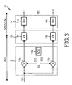
- the NCO of the first embodiment may be used in a digital down-converter as shown in Fig. 3.
- Fig. 3 is a block diagram showing the configuration of an embodiment of a digital down-converter 11 using the NCO of the first embodiment.
- multipliers 12b and 12c for multiplying the input signal by the real and imaginary components of
- a decimator 13 decimates the complex signal from the frequency converter 12.
- a roll-off filter 14 band-limits the complex signal decimated by the decimator 13 to a target signal band to output the resulting complex signal (I,Q).
- the roll-off filter 14 includes a real filter 14a and an imaginary filter 14b.
- the digital down-converter 11 is operated in the following manner.
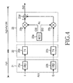
- the NCO of the first embodiment may also be used in a digital up-converter as shown in Fig. 4.
- Fig. 4 is a block diagram showing the configuration of an embodiment of a digital up-converter using the NCO of the first embodiment.
- the roll-off filter 21 includes a real filter 21a and an imaginary filter 21b.
- An interpolator 22 interpolates the complex signal band-limited by the roll-off filter 21.
- a frequency converter 23 frequency-converts an output signal from the interpolator 22 to output a real signal of a target center frequency Fif2.
- the digital up-converter is operated in the following manner.
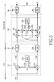
- Fig. 5 is a block diagram showing the configuration of the alternative embodiment of the digital down-converter using the numerical control oscillator of the first embodiment.
- the digital down-converter comprises a frequency converter 31 for frequency-converting an input signal of a center frequency Fif1 to obtain a complex signal of a center frequency Fif2.
- a decimator 32 decimates the complex signal from the frequency converter 31.
- a frequency converter 33 frequency-converts the complex signal decimated by the decimator 32 to obtain a complex signal of a center frequency Fif3.
- a roll-off filter 34 band-limits the complex signal from the frequency converter 33 to a target signal band to output the resulting complex signal (I,Q) of the center frequency Fif3.
- the roll-off filter 34 includes a real filter 34a and an imaginary filter 34b.
- the digital down-converter is operated in the following manner.
- the digital down-converter with the above-described configuration can convert the frequency of the input signal inputted thereto at the frequency setting interval FD into a desired frequency within the range of an allowable frequency deviation by means of only the frequency converter 31.
- the frequency conversion by the frequency converter 33 may be stopped.
- the digital down-converter with the above-stated configuration can have various settings of the respective parameters, including the above-described exemplary values, as shown in the below tables 2 to 5.
- the tables 2 and 3 show examples of settings of the respective parameters in a W-CDMA system
- the table 4 shows examples of settings of the respective parameters in an IS-95 Band (Class 0) system
- the table 5 shows examples of settings of the respective parameters in an IEEE 802.11a system.
- each frequency can be inputted by merely changing the setting of frequency data (phase difference data) to the NCO of the frequency converter 31. Therefore, a data setting time of a controller that controls the digital down-converter can be reduced by half compared with a conventional digital down-converter requiring the setting of data to both frequency converters and the frequency data to the NCO can be computed in a simpler manner.
- the digital down-converter in which the frequency setting interval dF of the input signal is 200KHz can set the phase difference data ⁇ to 132 for the lower IF limit, and to 232 for the upper IF limit by incrementing the phase difference data ⁇ by "1" whenever changing the IF by 200KHz.
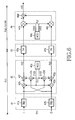
- the NCO of the first embodiment may be used in a digital up-converter as shown in Fig. 6.
- the digital up-converter comprises a first frequency converter, and a second frequency converter including the NCO as a local oscillator, and serves to perform two frequency conversions to convert an input signal into a signal with a frequency higher than that of the input signal and output the converted signal as a signal sampled at a sampling frequency Fs.
- Fig. 6 is a block diagram showing the configuration of an alternative embodiment of the digital up-converter using the NCO of the first embodiment.
- the roll-off filter 41 includes a real filter 41 a and an imaginary filter 41b.
- a frequency converter 42 frequency-converts an output signal from the roll-off filter 41 to obtain a complex signal of a center frequency Fif2.
- An interpolator 43 interpolates the complex signal from the frequency converter 42.
- a frequency converter 44 frequency-converts an output signal from the interpolator 43 to output a real signal of a target center frequency Fif3.
- a local oscillator 44a using the NCO of the first embodiment
- the digital up-converter is operated in the following manner.
- the digital up-converter is operated in the following manner.
- the digital up-converter in the case where a multiple of the frequency setting interval FD2 of the frequency converter 44 is equal to that of the frequency setting interval FD of the output signal, the digital up-converter with the above-described configuration can set the frequency setting interval of its output signal to FD by means of only the frequency converter 44. In this case, the frequency conversion by the frequency converter 42 may be stopped.
- each frequency in the case where the frequency setting interval FD2 of the frequency converter 44 is settable at a step lower than or equal to the desired frequency setting interval FD of the output signal, each frequency can be inputted by merely changing the setting of frequency data (phase difference data) to the NCO of the frequency converter 44. Therefore, a data setting time of a controller that controls the digital up-converter can be reduced by half compared with a conventional digital up-converter requiring the setting of data to both frequency converters and the frequency data to the NCO can be computed in a simpler manner.
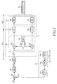
- Fig. 7 is a block diagram showing the configuration of an embodiment of a receiver using the NCO of the first embodiment.
- the receiver comprises a local oscillator 51 including the NCO 51a of the first embodiment, a digital to analog converter (DAC) 51b for digital/analog-converting an output signal from the NCO 51a, and a PLL circuit 51 c for receiving an output signal from the DAC 51b as a reference signal.
- DAC digital to analog converter
- a frequency setting step FDP of the analog local signal (frequency setting interval of the mixer 52) is a multiplication of a frequency setting step FD of the NCO 51a by P.
- a band pass filter 53 has a pass frequency band characteristic corresponding to a frequency band of the analog IF signal and acts to extract the analog IF signal from the mixer 52 and output it to an analog to digital converter (ADC) 54.
- ADC analog to digital converter
- the ADC 54 quantizes the analog IF signal from the band pass filter 53 and generates a ⁇ Sub-Nyquist sampled ⁇ digital IF signal of a center frequency Fif2.
- the digital down-converter 11 of Fig. 3 is used to convert an output signal from the ADC 54 into a complex signal (I,Q) of a frequency desired by a demodulator 55 and output the converted complex signal to the demodulator 55.
- the demodulator 55 demodulates the output signal from the digital down-converter 11 to extract received data therefrom.
- the receiver is operated in the following manner.
- the receiver with the above-described configuration can convert the frequency of the received signal inputted thereto at the frequency setting interval FD into that desired by the demodulator 55 by means of only the mixer 52. In this case, the frequency conversion by the frequency converter 12 may be stopped.
- the receiver with the above-stated configuration can have various settings of the respective parameters as shown in the below tables 6 to 9.
- the tables 6 and 7 show examples of settings of the respective parameters in a W-CDMA system
- the table 8 shows examples of settings of the respective parameters in an IS-95 Band (Class 0) system
- the table 9 shows examples of settings of the respective parameters in an IEEE 802.11 a system. No.
- each frequency can be inputted by merely changing the setting of frequency data (phase difference data) to the NCO of the local oscillator 51. Therefore, a data setting time of a controller that controls the receiver can be reduced compared with a conventional receiver and the frequency data to the NCO can be computed in a simpler manner.
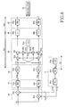
- Fig. 8 is a block diagram showing the configuration of an alternative embodiment of the receiver using the NCO of the first embodiment, wherein a quadrature demodulator 82 is used instead of the mixer 52 of the receiver shown in Fig. 7 to quadrature-demodulate an analog version of a received signal.
- the receiver comprises a local oscillator 81 including the NCO 81 a of the first embodiment, a DAC 81b for digital/analog-converting an output signal from the NCO 81a, and a PLL circuit 81 c for receiving an output signal from the DAC 81b as a reference signal.
- the quadrature demodulator 82 includes a real mixer 82a and an imaginary mixer 82b.
- a frequency setting step FDP of the analog local signal (frequency setting interval of the quadrature demodulator 82) is a multiplication of a frequency setting step FD of the NCO 81 a by P.
- a band pass filter 83 has a pass frequency band characteristic corresponding to a frequency band of the analog IF complex signal and acts to extract the analog IF complex signal from the quadrature demodulator 82 and output it to an ADC 84.
- the band pass filter 83 includes a real band pass filter 83a and an imaginary band pass filter 83b.
- the ADC 84 quantizes the analog IF complex signal from the band pass filter 83 and generates a digital IF signal of a center frequency Fif2. To this end, the ADC 84 includes a real ADC 84a and an imaginary ADC 84b.
- a frequency converter 85 frequency-converts an output signal from the ADC 84.
- a decimator 86 decimates a complex signal from the frequency converter 85.
- a roll-off filter 87 band-limits an output signal from the decimator 86 to a target signal band and outputs the resulting complex signal (I,Q) of the frequency desired by the demodulator 55 thereto.
- the roll-off filter 87 includes a real filter 87a and an imaginary filter 87b.
- the NCO 81a, local oscillator 81, local oscillator 85a and frequency converter 85 perform the same operations as those of the NCO 51a, local oscillator 51, local oscillator 12a and frequency converter 12 in the receiver previously stated with reference to Fig. 7 on the basis of the relations between the desired frequency setting interval FD of the received signal and the frequency setting interval FDP of the quadrature demodulator 82, respectively.
- the receiver with the above-described configuration can convert the frequency of the received signal inputted thereto at the frequency setting interval FD into that desired by the demodulator by means of only the quadrature demodulator 82.
- the frequency conversion by the frequency converter 85 may be stopped.
- the receiver with the above-stated configuration can have various settings of the respective parameters as shown in the below tables 10 to 13.
- the tables 10 and 11 show examples of settings of the respective parameters in a W-CDMA system
- the table 12 shows examples of settings of the respective parameters in an IS-95 Band (Class 0) system
- the table 13 shows examples of settings of the respective parameters in an IEEE 802.11 a system. No.
- each frequency can be inputted by merely changing the setting of frequency data (phase difference data) to the NCO of the local oscillator 81. Therefore, a data setting time of a controller that controls the receiver can be reduced compared with a conventional receiver and the frequency data to the NCO can be computed in a simpler manner.
- the center frequency Fifa of the analog IF complex signal can be set to a lower value, thereby making it possible to apply a relatively small number of phase amplitude data to the local oscillator 85a using the NCO of the first embodiment, constructing the downstream frequency converter 85.
- the NCO of the first embodiment may also be used in a transmitter as shown in Fig. 9.
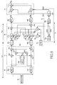
- Fig. 9 is a block diagram showing the configuration of a transmitter using the NCO of the first embodiment.
- the transmitter comprises a modulator 61 for modulating a carrier based on transmit data to be transmitted from the transmitter, and a roll-off filter 62 for band-limiting a complex signal (containing baseband signal components I and Q) outputted from the modulator 61 to a target signal band.
- the roll-off filter 62 includes a real filter 62a and an imaginary filter 62b.
- a frequency converter 63 frequency-converts an output signal from the roll-off filter 62 to obtain a complex signal of a center frequency Fif2.
- An interpolation band pass filter 68 interpolates and band pass filters the complex signal from the frequency converter 63.
- a real DAC 69a and imaginary DAC 69b cooperate to convert a digital signal of the center frequency Fif2 from the interpolation band pass filter 68 into a complex analog IF signal of a center frequency Fifa.
- a local oscillator 70 includes the NCO 70a of the first embodiment, a DAC 70b for digital/analog-converting an output signal from the NCO 70a, and a PLL circuit 70c for receiving an output signal from the DAC 70b as a reference signal.
- a quadrature modulator 71 frequency-converts the complex analog IF signal of the center frequency Fifa from the real DAC 69a and imaginary DAC 69b to output a transmit signal (real signal) of a target center frequency Frf.
- a frequency setting step FDP of the analog local signal (frequency setting interval of the quadrature modulator 71) is a multiplication of a frequency setting step FD of the NCO 70a by P.
- the transmitter is operated in the following manner.
- K1, K2 and L2 are arbitrary integers
- the transmitter is operated in the following manner.
- the transmitter with the above-described configuration can frequency-convert the transmit signal into the transmit signal (real signal) of the target center frequency Frf by means of only the quadrature modulator 71.
- the frequency conversion by the frequency converter 63 may be stopped.
- each frequency can be outputted by merely changing the setting of frequency data (phase difference data) to the NCO of the local oscillator 70. Therefore, a data setting time of a controller that controls the transmitter can be reduced compared with a conventional transmitter and the frequency data to the NCO can be computed in a simpler manner.
- the phase calculator 1b generates phase data by performing a modulo operation taking the integral M as a modulus with respect to input phase difference data and phase data from the phase register 1a.
- a low-spurious NCO which provides its output signal set to a frequency setting interval lower than or equal to a desired frequency setting interval is realized on the basis of only low-capacity, amplitude data of M number that is smaller than a conventional one, it can be reduced in power consumption and cost.
- the digital down-converter, the digital up-converter, the receiver with the demodulator and the transmitter with the modulator of the second to eighth embodiments using the NCO of the first embodiment.
- the digital down-converter, digital up-converter, receiver or transmitter can be reduced in power consumption and cost compared with a conventional one.
- a low-spurious NCO which provides its output signal set to a frequency setting interval lower than or equal to a desired frequency setting interval can be realized on the basis of only low-capacity, amplitude data of M number that is smaller than a conventional one, so it can be reduced in power consumption and cost.
- a desired frequency setting interval FD of the input signal is higher than or equal to a frequency setting interval dF of the frequency converter and is evenly divisible by it
- the digital down-converter can convert the frequency of the input signal inputted thereto at the frequency setting interval FD into a desired frequency within the range of an allowable frequency deviation.
- one of two frequency converters provided for frequency conversions includes a low-spurious NCO which is realized on the basis of only M1 low-capacity amplitude data and provides its output signal set to a frequency setting interval lower than or equal to a desired frequency setting interval, and the other includes a low-spurious NCO which is realized on the basis of only M2 low-capacity amplitude data and provides its output signal set to a frequency setting interval lower than or equal to a desired frequency setting interval.
- the digital down-converter is able to cope with the case where a frequency setting interval FD of an input signal is above a frequency setting interval FD1 of the first frequency converter and is indivisible by it, the case where the frequency setting interval FD is below the frequency setting interval FD1 and FD1 is indivisible by FD, and the case where the frequency setting interval FD is higher than or equal to the frequency setting interval FD1 and is evenly divisible by it, or FD is lower than FD1 and FD1 is evenly divisible by FD, respectively.
- the use of the two low-spurious NCOs which are realized on the basis of only low-capacity, amplitude data of M1 and M2 numbers that are each smaller than a conventional one and provide their output signals each set to a frequency setting interval lower than or equal to a desired frequency setting interval can reduce power consumption and cost of the digital down-converter that can convert the frequency of the input signal inputted thereto at the desired frequency setting interval into a desired frequency within the range of an allowable frequency deviation.
- the digital down-converter in the case where a multiple of the frequency setting interval FD1 of the first frequency converter is equal to that of the frequency setting interval FD of the input signal, the digital down-converter can convert the frequency of the input signal inputted thereto at the frequency setting interval FD into a desired frequency within the range of an allowable frequency deviation by means of only the first frequency converter.
- a desired frequency setting interval FD of an output signal is higher than or equal to a frequency setting interval dF of the frequency converter and is evenly divisible by it, the digital up-converter can set the frequency setting interval of its output signal to FD.
- one of two frequency converters provided for frequency conversions includes a low-spurious NCO which is realized on the basis of only M1 low-capacity amplitude data and provides its output signal set to a frequency setting interval lower than or equal to a desired frequency setting interval, and the other includes a low-spurious NCO which is realized on the basis of only M2 low-capacity amplitude data and provides its output signal set to a frequency setting interval lower than or equal to a desired frequency setting interval.
- the digital up-converter is able to cope with the case where a frequency setting interval FD of an output signal is above a frequency setting interval FD2 of the second frequency converter and is indivisible by it, the case where the frequency setting interval FD is below the frequency setting interval FD2 and FD2 is indivisible by FD, and the case where the frequency setting interval FD is higher than or equal to the frequency setting interval FD2 and is evenly divisible by it, or FD is lower than FD2 and FD2 is evenly divisible by FD, respectively.
- the use of the two low-spurious NCOs which are realized on the basis of only low-capacity, amplitude data of M1 and M2 numbers that are each smaller than a conventional one and provide their output signals each set to a frequency setting interval lower than or equal to a desired frequency setting interval can reduce power consumption and cost of the digital up-converter that can output a signal of the desired frequency setting interval.
- the digital up-converter in the case where a multiple of the frequency setting interval FD2 of the second frequency converter is equal to that of the frequency setting interval FD of the output signal, the digital up-converter can set the frequency setting interval of its output signal to FD by means of only the second frequency converter.
- one of two frequency converters provided for frequency conversion of a received signal into an input signal desired by a demodulator includes a low-spurious NCO which is realized on the basis of only M1 low-capacity amplitude data and provides its output signal set to a frequency setting interval lower than or equal to a desired frequency setting interval, and the other includes a low-spurious NCO which is realized on the basis of only M2 low-capacity amplitude data and provides its output signal set to a frequency setting interval lower than or equal to a desired frequency setting interval.
- the receiver is able to cope with the case where a frequency setting interval FD of an input signal is above a frequency setting interval FDP of the first frequency converter and is indivisible by it, the case where the frequency setting interval FD is below the frequency setting interval FDP and FDP is indivisible by FD, and the case where the frequency setting interval FD is higher than or equal to the frequency setting interval FDP and is evenly divisible by it, or FD is lower than FDP and FDP is evenly divisible by FD, respectively.
- the use of the two low-spurious NCOs which are realized on the basis of only low-capacity, amplitude data of M1 and M2 numbers that are each smaller than a conventional one and provide their output signals each set to a frequency setting interval lower than or equal to a desired frequency setting interval can reduce power consumption and cost of the receiver that can accurately convert the frequency of the received signal inputted thereto at the frequency setting interval FD into that desired by the demodulator.
- the receiver in the case where a multiple of the frequency setting interval FD1 of the first frequency converter is equal to that of the frequency setting interval FD of the received signal, the receiver can accurately convert the frequency of the received signal inputted thereto at the frequency setting interval FD into that desired by the demodulator by means of only the first frequency converter.
- one of two frequency converters provided for frequency conversion of a transmit signal from a modulator into a target frequency includes a low-spurious NCO which is realized on the basis of only M1 low-capacity amplitude data and provides its output signal set to a frequency setting interval lower than or equal to a desired frequency setting interval, and the other includes a low-spurious NCO which is realized on the basis of only M2 low-capacity amplitude data and provides its output signal set to a frequency setting interval lower than or equal to a desired frequency setting interval.
- the transmitter is able to cope with the case where a frequency setting interval FD of an output signal is above a frequency setting interval FDP of the second frequency converter and is indivisible by it, the case where the frequency setting interval FD is below the frequency setting interval FDP and FDP is indivisible by FD, and the case where the frequency setting interval FD is higher than or equal to the frequency setting interval FDP and is evenly divisible by it, or FD is lower than FDP and FDP is evenly divisible by FD, respectively.
- the use of the two low-spurious NCOs which are realized on the basis of only low-capacity, amplitude data of M1 and M2 numbers that are each smaller than a conventional one and provide their output signals each set to a frequency setting interval lower than or equal to a desired frequency setting interval can reduce power consumption and cost of the transmitter that can accurately convert the frequency of the baseband transmit signal from the modulator into a target transmit signal frequency.
- the transmitter in the case where a multiple of the frequency setting interval FD2 of the second frequency converter is equal to that of the frequency setting interval FD of the transmit signal, the transmitter can accurately convert the frequency of the baseband transmit signal from the modulator into that of a target transmit signal by means of only the second frequency converter.
Landscapes
- Engineering & Computer Science (AREA)
- Theoretical Computer Science (AREA)
- Power Engineering (AREA)
- Physics & Mathematics (AREA)
- General Engineering & Computer Science (AREA)
- General Physics & Mathematics (AREA)
- Stabilization Of Oscillater, Synchronisation, Frequency Synthesizers (AREA)
- Transmitters (AREA)
Applications Claiming Priority (2)
| Application Number | Priority Date | Filing Date | Title |
|---|---|---|---|
| JP2002359773 | 2002-12-11 | ||
| JP2002359773A JP2004193996A (ja) | 2002-12-11 | 2002-12-11 | 数値制御発振器、ディジタル周波数コンバータ及び無線機 |
Publications (1)
| Publication Number | Publication Date |
|---|---|
| EP1429231A1 true EP1429231A1 (de) | 2004-06-16 |
Family
ID=32322108
Family Applications (1)
| Application Number | Title | Priority Date | Filing Date |
|---|---|---|---|
| EP03028172A Ceased EP1429231A1 (de) | 2002-12-11 | 2003-12-08 | Digital gesteuerter Oszillator, Digitaler Frequenzwandler und Funkfrequenzeinheit |
Country Status (4)
| Country | Link |
|---|---|
| US (1) | US7308240B2 (de) |
| EP (1) | EP1429231A1 (de) |
| JP (1) | JP2004193996A (de) |
| KR (1) | KR100605887B1 (de) |
Cited By (3)
| Publication number | Priority date | Publication date | Assignee | Title |
|---|---|---|---|---|
| GB2440187A (en) * | 2006-07-17 | 2008-01-23 | Ubidyne Inc | DUC and DDC forming digital transceiver |
| CN102098470B (zh) * | 2009-12-11 | 2013-01-16 | 无锡华润矽科微电子有限公司 | 一种查表优化方法及数字控制振荡器 |
| CN105929889A (zh) * | 2016-04-22 | 2016-09-07 | 威胜集团有限公司 | 波形的直接数字频率合成方法 |
Families Citing this family (11)
| Publication number | Priority date | Publication date | Assignee | Title |
|---|---|---|---|---|
| JP2004193996A (ja) * | 2002-12-11 | 2004-07-08 | Samsung Electronics Co Ltd | 数値制御発振器、ディジタル周波数コンバータ及び無線機 |
| US20050265483A1 (en) * | 2004-05-25 | 2005-12-01 | Berkana Wireless, Inc. | Digital noise coupling reduction and variable intermediate frequency generation in mixed signal circuits |
| KR100656318B1 (ko) | 2004-08-05 | 2006-12-11 | 한국전자통신연구원 | 디지털 사인 파형을 생성하는 수치 제어 발진 방법 및 그장치 |
| FR2900006B1 (fr) * | 2006-04-13 | 2013-09-20 | St Microelectronics Sa | Recepteur de signal radio, du type a frequence intermediaire |
| US20090163162A1 (en) * | 2007-12-19 | 2009-06-25 | Hoffman Stephen W | Direct conversion receiving architecture with an integrated tuner self alignment function |
| US8068563B2 (en) * | 2008-10-20 | 2011-11-29 | Ibiquity Digital Corporation | Systems and methods for frequency offset correction in a digital radio broadcast receiver |
| JP5931204B2 (ja) | 2012-08-13 | 2016-06-08 | 三菱電機株式会社 | 信号生成装置 |
| CN107885276B (zh) * | 2017-12-27 | 2023-09-01 | 南京天际易达通信技术有限公司 | 一种波形生成方法及生成装置 |
| KR102887955B1 (ko) | 2020-10-15 | 2025-11-19 | 삼성전자주식회사 | 무선 통신 시스템에서 다수의 사업자를 지원하는 네트워크 공유 방법 및 장치. |
| CN113359923A (zh) * | 2021-06-23 | 2021-09-07 | 吉林大学 | 数控直流稳压电源 |
| CN114779876B (zh) * | 2022-04-15 | 2024-03-22 | 中国电子科技集团公司第五十八研究所 | 一种高速高精度数控振荡器 |
Citations (7)
| Publication number | Priority date | Publication date | Assignee | Title |
|---|---|---|---|---|
| US5202846A (en) * | 1990-12-19 | 1993-04-13 | Hughes Aircraft Company | Prime number spur reduction for digital synthesis |
| US5371765A (en) * | 1992-07-10 | 1994-12-06 | Hewlett-Packard Company | Binary phase accumulator for decimal frequency synthesis |
| DE4440510A1 (de) * | 1994-11-12 | 1996-05-30 | Ant Nachrichtentech | Verfahren zur Erzeugung eines digitalen Sinussignales |
| US5619535A (en) * | 1994-07-27 | 1997-04-08 | Alvarez, Jr.; Cesar E. | Digital frequency synthesizer |
| EP0907121A2 (de) * | 1997-10-01 | 1999-04-07 | Ford Motor Company | Digitaler Oszillator mit eienr Mehrzyklennachschlagetabelle |
| US20020048325A1 (en) * | 2000-09-21 | 2002-04-25 | Samsung Electronics Co., Ltd. | Digital down-converter |
| US6463266B1 (en) * | 1999-08-10 | 2002-10-08 | Broadcom Corporation | Radio frequency control for communications systems |
Family Cites Families (14)
| Publication number | Priority date | Publication date | Assignee | Title |
|---|---|---|---|---|
| US4860018A (en) * | 1982-03-01 | 1989-08-22 | Western Atlas International, Inc. | Continuous wave interference rejection for reconstructed carrier receivers |
| US4870422A (en) * | 1982-03-01 | 1989-09-26 | Western Atlas International, Inc. | Method and system for determining position from signals from satellites |
| GB2228840B (en) * | 1989-03-04 | 1993-02-10 | Racal Dana Instr Ltd | Frequency synthesisers |
| FR2741173B1 (fr) * | 1995-11-10 | 1997-12-05 | Sextant Avionique | Multiplieur rapide pour multiplier un signal numerique par un signal periodique |
| US6308048B1 (en) * | 1997-11-19 | 2001-10-23 | Ericsson Inc. | Simplified reference frequency distribution in a mobile phone |
| US6584145B1 (en) * | 1999-06-02 | 2003-06-24 | Level One Communications, Inc. | Sample rate converter |
| KR100652028B1 (ko) * | 1999-07-13 | 2006-11-30 | 엘지전자 주식회사 | 다매체 디지털 방송 수신기의 락 디텍트(lock detect)장치 |
| US6236278B1 (en) * | 2000-02-16 | 2001-05-22 | National Semiconductor Corporation | Apparatus and method for a fast locking phase locked loop |
| CN1166226C (zh) | 2000-11-23 | 2004-09-08 | 华为技术有限公司 | 数字本振信号产生方法及数字控制振荡器 |
| CA2387891A1 (en) * | 2001-06-08 | 2002-12-08 | Asulab S.A. | Radiofrequency signal receiver with means for correcting the effects of multipath signals, and method for activating the receiver |
| US6781473B1 (en) * | 2001-09-14 | 2004-08-24 | Broadlogic Network Technologies, Inc. | High-speed low-power implementation for multi-channel numerically controlled oscillator (NCO) |
| TWI237971B (en) * | 2002-11-18 | 2005-08-11 | Ind Tech Res Inst | Automatically adjusting gain/bandwidth loop filter |
| JP2004193996A (ja) * | 2002-12-11 | 2004-07-08 | Samsung Electronics Co Ltd | 数値制御発振器、ディジタル周波数コンバータ及び無線機 |
| US7064616B2 (en) * | 2003-12-29 | 2006-06-20 | Teradyne, Inc. | Multi-stage numeric counter oscillator |
-
2002
- 2002-12-11 JP JP2002359773A patent/JP2004193996A/ja active Pending
-
2003
- 2003-12-08 EP EP03028172A patent/EP1429231A1/de not_active Ceased
- 2003-12-11 US US10/733,526 patent/US7308240B2/en not_active Expired - Fee Related
- 2003-12-11 KR KR1020030090251A patent/KR100605887B1/ko not_active Expired - Fee Related
Patent Citations (7)
| Publication number | Priority date | Publication date | Assignee | Title |
|---|---|---|---|---|
| US5202846A (en) * | 1990-12-19 | 1993-04-13 | Hughes Aircraft Company | Prime number spur reduction for digital synthesis |
| US5371765A (en) * | 1992-07-10 | 1994-12-06 | Hewlett-Packard Company | Binary phase accumulator for decimal frequency synthesis |
| US5619535A (en) * | 1994-07-27 | 1997-04-08 | Alvarez, Jr.; Cesar E. | Digital frequency synthesizer |
| DE4440510A1 (de) * | 1994-11-12 | 1996-05-30 | Ant Nachrichtentech | Verfahren zur Erzeugung eines digitalen Sinussignales |
| EP0907121A2 (de) * | 1997-10-01 | 1999-04-07 | Ford Motor Company | Digitaler Oszillator mit eienr Mehrzyklennachschlagetabelle |
| US6463266B1 (en) * | 1999-08-10 | 2002-10-08 | Broadcom Corporation | Radio frequency control for communications systems |
| US20020048325A1 (en) * | 2000-09-21 | 2002-04-25 | Samsung Electronics Co., Ltd. | Digital down-converter |
Cited By (7)
| Publication number | Priority date | Publication date | Assignee | Title |
|---|---|---|---|---|
| GB2440187A (en) * | 2006-07-17 | 2008-01-23 | Ubidyne Inc | DUC and DDC forming digital transceiver |
| WO2008009422A2 (en) | 2006-07-17 | 2008-01-24 | Ubidyne Inc. | Digital transceiver |
| WO2008009422A3 (en) * | 2006-07-17 | 2008-06-12 | Ubidyne Inc | Digital transceiver |
| US8300724B2 (en) | 2006-07-17 | 2012-10-30 | Ubidyne, Inc. | Digital transceiver |
| CN102098470B (zh) * | 2009-12-11 | 2013-01-16 | 无锡华润矽科微电子有限公司 | 一种查表优化方法及数字控制振荡器 |
| CN105929889A (zh) * | 2016-04-22 | 2016-09-07 | 威胜集团有限公司 | 波形的直接数字频率合成方法 |
| CN105929889B (zh) * | 2016-04-22 | 2018-09-25 | 威胜集团有限公司 | 波形的直接数字频率合成方法 |
Also Published As
| Publication number | Publication date |
|---|---|
| KR100605887B1 (ko) | 2006-08-01 |
| KR20040051560A (ko) | 2004-06-18 |
| JP2004193996A (ja) | 2004-07-08 |
| US7308240B2 (en) | 2007-12-11 |
| US20040120425A1 (en) | 2004-06-24 |
Similar Documents
| Publication | Publication Date | Title |
|---|---|---|
| JP2926615B2 (ja) | Ssb信号発生器 | |
| EP1429231A1 (de) | Digital gesteuerter Oszillator, Digitaler Frequenzwandler und Funkfrequenzeinheit | |
| JP4652546B2 (ja) | 受信機 | |
| US8532162B2 (en) | Transceiver front end for software radio system | |
| JP2001502154A (ja) | ディジタル通信装置及びミクサ | |
| JP4633902B2 (ja) | デジタルダウンコンバータ | |
| KR20020006044A (ko) | 프로그래머블 디지털 중간 주파수 송수신기 | |
| KR20030043905A (ko) | 이동 통신용 수신기 | |
| US6347123B1 (en) | Low-current sample rate converter | |
| KR100901692B1 (ko) | 저속 무선 개인 통신 네트워크에서 다중모드 송수신 장치및 그 방법 | |
| JP2006121665A (ja) | イメージリジェクションミキサと能動帯域フィルタを有する受信if回路 | |
| JP2003298456A (ja) | ソフトウェア無線機及びソフトウェア無線機の信号処理方法 | |
| US7751303B2 (en) | Demodulation circuit for use in receiver using if directing sampling scheme | |
| US8036625B1 (en) | Method and apparatus for mixing a signal | |
| US6570939B1 (en) | Receiving device with demodulating function based on orthogonal detection and equalizing function based on maximum likelihood sequence estimation | |
| JPH11196016A (ja) | 周波数変換器と周波数変換方法 | |
| JP3454724B2 (ja) | 復調回路 | |
| JP2006319398A (ja) | 受信機および受信方法 | |
| KR20010041140A (ko) | 무선 주파수 신호의 전송 회로, 무선전화 장치 및 주파수변환기 | |
| JP2005151477A (ja) | 送信装置及びそれに用いるデジタル直交変調回路 | |
| JP2007215039A (ja) | 周波数シンセサイザ、通信機、及び周波数シンセサイズ方法 | |
| JPH10136045A (ja) | 復調装置および通信端末装置 | |
| JPH1141134A (ja) | 可変レート無線機 | |
| JP2000286724A (ja) | 無線通信機の送信部構成方式 | |
| JP2005252931A (ja) | 直交変調器 |
Legal Events
| Date | Code | Title | Description |
|---|---|---|---|
| PUAI | Public reference made under article 153(3) epc to a published international application that has entered the european phase |
Free format text: ORIGINAL CODE: 0009012 |
|
| 17P | Request for examination filed |
Effective date: 20031208 |
|
| AK | Designated contracting states |
Kind code of ref document: A1 Designated state(s): AT BE BG CH CY CZ DE DK EE ES FI FR GB GR HU IE IT LI LU MC NL PT RO SE SI SK TR |
|
| AX | Request for extension of the european patent |
Extension state: AL LT LV MK |
|
| AKX | Designation fees paid |
Designated state(s): DE FR GB |
|
| 17Q | First examination report despatched |
Effective date: 20051026 |
|
| STAA | Information on the status of an ep patent application or granted ep patent |
Free format text: STATUS: THE APPLICATION HAS BEEN REFUSED |
|
| 18R | Application refused |
Effective date: 20080204 |