EP1429372A1 - Vorrichtung und Verfahren zur Entfernung von dünnschichtigen Halbleiterstrukturen - Google Patents
Vorrichtung und Verfahren zur Entfernung von dünnschichtigen Halbleiterstrukturen Download PDFInfo
- Publication number
- EP1429372A1 EP1429372A1 EP03078070A EP03078070A EP1429372A1 EP 1429372 A1 EP1429372 A1 EP 1429372A1 EP 03078070 A EP03078070 A EP 03078070A EP 03078070 A EP03078070 A EP 03078070A EP 1429372 A1 EP1429372 A1 EP 1429372A1
- Authority
- EP
- European Patent Office
- Prior art keywords
- die
- film
- ejector
- less
- thickness
- Prior art date
- Legal status (The legal status is an assumption and is not a legal conclusion. Google has not performed a legal analysis and makes no representation as to the accuracy of the status listed.)
- Withdrawn
Links
Images

Classifications
-
- H—ELECTRICITY
- H10—SEMICONDUCTOR DEVICES; ELECTRIC SOLID-STATE DEVICES NOT OTHERWISE PROVIDED FOR
- H10P—GENERIC PROCESSES OR APPARATUS FOR THE MANUFACTURE OR TREATMENT OF DEVICES COVERED BY CLASS H10
- H10P54/00—Cutting or separating of wafers, substrates or parts of devices
-
- H—ELECTRICITY
- H10—SEMICONDUCTOR DEVICES; ELECTRIC SOLID-STATE DEVICES NOT OTHERWISE PROVIDED FOR
- H10P—GENERIC PROCESSES OR APPARATUS FOR THE MANUFACTURE OR TREATMENT OF DEVICES COVERED BY CLASS H10
- H10P72/00—Handling or holding of wafers, substrates or devices during manufacture or treatment thereof
- H10P72/04—Apparatus for manufacture or treatment
- H10P72/0442—Apparatus for placing on an insulating substrate, e.g. tape
-
- H—ELECTRICITY
- H10—SEMICONDUCTOR DEVICES; ELECTRIC SOLID-STATE DEVICES NOT OTHERWISE PROVIDED FOR
- H10P—GENERIC PROCESSES OR APPARATUS FOR THE MANUFACTURE OR TREATMENT OF DEVICES COVERED BY CLASS H10
- H10P72/00—Handling or holding of wafers, substrates or devices during manufacture or treatment thereof
- H10P72/04—Apparatus for manufacture or treatment
- H10P72/0428—Apparatus for mechanical treatment or grinding or cutting
-
- H—ELECTRICITY
- H10—SEMICONDUCTOR DEVICES; ELECTRIC SOLID-STATE DEVICES NOT OTHERWISE PROVIDED FOR
- H10P—GENERIC PROCESSES OR APPARATUS FOR THE MANUFACTURE OR TREATMENT OF DEVICES COVERED BY CLASS H10
- H10P72/00—Handling or holding of wafers, substrates or devices during manufacture or treatment thereof
- H10P72/70—Handling or holding of wafers, substrates or devices during manufacture or treatment thereof for supporting or gripping
- H10P72/74—Handling or holding of wafers, substrates or devices during manufacture or treatment thereof for supporting or gripping using temporarily an auxiliary support
- H10P72/7412—Handling or holding of wafers, substrates or devices during manufacture or treatment thereof for supporting or gripping using temporarily an auxiliary support the auxiliary support including means facilitating the separation of a device or wafer from the auxiliary support
- H10P72/7414—Handling or holding of wafers, substrates or devices during manufacture or treatment thereof for supporting or gripping using temporarily an auxiliary support the auxiliary support including means facilitating the separation of a device or wafer from the auxiliary support the auxiliary support including means facilitating the selective separation of some of a plurality of devices from the auxiliary support
Definitions
- This invention relates to an apparatus and method of using multiple ejector pins located at specific locations with respect to a die for the detachment of thin dice during die bonding of electronic packages.
- wafers comprising arrays of semiconductor dice are usually received after dicing on a film frame, and are fed to die bonding machines for placement.
- dice are detached and lifted from a film frame comprising plastic adhesive film or a Mylar film and are then transferred to a substrate such as a lead frame or printed wiring board (PWB) substrate.
- PWB printed wiring board
- a designated die will first be aligned and moved to a location where push-up pins will rise to raise a die from below while the plastic adhesive film is held down by vacuum suction.
- a collet or pick-up tool is then moved to just above the top surface of the die.
- the die will be detached from the plastic adhesive film when the push-up pins rise to an appropriate level.
- the collet provides vacuum suction to hold the die during the action of transferring the die from the plastic adhesive film to the bonding substrate.
- a prior art pick-up process includes a typical push-up mechanism using one ejector pin or multiple ejector pins.
- Fig. 1 shows a typical layout of the push-up device and its peripheral devices.
- hole(s) on a cap connected to a vacuum suction supply is used to hold a designated die and the plastic adhesive film in position during the die detachment process.
- a chuck Inside the cap of the vacuum ejector platform, a chuck holds ejector pins and is connected to a motorized mechanism that provides a vertical pushing motion for the ejector pins. During the push-up motion, the ejector pins move upward and push onto a die and the plastic adhesive film.
- the die mounted on the plastic adhesive film starts to be delaminated and separates from the film.
- the adhesive force and adhered area between the die and plastic adhesive film are small enough such that it is possible for the pick-up collet to pull the die away from the film by suction means.
- US patent number 5,755,373 for a "Die Push-Up Device” uses a die push-up device with only one push-up ejector pin in a bonding machine for semiconductor devices. This invention is applicable for small and thick dice (say, more than 0.2 mm thick). As the size of the die gets bigger (say, more than 5 mm in width), a two-stage ejecting process (such as that in US patent number 4,850,780 for a "Pre-Peel Die Ejector Apparatus”) may be used. In relation to US patent number 5,755,373, using a single ejector pin to perform the die detachment process will not be practical if a thin (less than 0.1mm thick) and large die (more than 4 mm width) is involved.
- an apparatus for thin die detachment comprising: a film having an adhesive surface on which a plurality of dice are mountable; a collet for holding and detaching a die mounted on the adhesive surface; and an ejector device comprising a plurality of ejector pins, each ejector pin operative to contact and raise a second surface of the film opposite the adhesive surface at a position substantially at a corner of the die to be detached within a predetermined distance from the edges of said die, whereby to partially delaminate said die from the adhesive surface for detachment by the collet.
- a method of detaching a thin die mounted on an adhesive surface of a film comprising the steps of: contacting and raising a second surface of the film opposite the adhesive surface with a plurality of ejector pins at positions substantially at the corners of the die within a predetermined distance from the edges of said die; pushing against the film at positions substantially at the corners of the die to partially delaminate the die; and holding the partially-delaminated die and detaching the die from the adhesive surface.
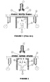
- FIG. 1 An ejector device and its peripheral devices for a die detachment process of the prior art are shown in Fig. 1.
- a plurality of dice 3 are singulated and attached to a plastic adhesive film 4.
- the plastic adhesive film 4 is mounted to a wafer table with expander (not shown) that moves the dice 3 with respect to a vacuum ejector platform 8.
- This vacuum ejector platform 8 is an enclosure containing a mechanism driving a chuck 7 supporting one or more ejector pins 6.
- the chuck 7 provides the mounting hoies and brackets for the ejector pins 6 and it is driven up and down by a motorized mechanism (not shown). Moving a die 3 designated to be picked up to the center of the vacuum ejector platform 8 starts a pick-up cycle.
- the plastic adhesive film 4 is held down against the top surface of the platform 8 by vacuum suction connected to a vacuum suction supply 9 via a hole 5 at the top of the vacuum ejector platform 8 and a periphery of the plastic adhesive film 4 is held down by additional vacuum suction provided through an outer ring 10.
- the ejector pins 6 that rise above the top surface of the vacuum ejector platform 8 will lift up the die 3 on the plastic adhesive film 4.
- a collet 2 moves down and rests on top of the die 3 with its suction vacuum supply 1 on, to hold and detach the die 3 from the adhesive film 4.
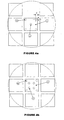
- the designated die is pushed up either by one ejector pin or multiple ejector pins as shown in Figs. 2a and 2b, or by a two-stage push-up motion (as in US patent number 4,850,780).
- a two-stage push-up motion (as in US patent number 4,850,780).
- US patent number 4,850,780 There is no particular arrangement of the pins.
- the prior art is suitable for the detachment of small and thick dice. With dice getting thinner and their sizes getting bigger, there is a very high chance that a die will crack and break into two or more pieces during a die detachment process when the ejector pins 6 push up against the die 3 on the plastic adhesive film 4.
- An ejector device and its peripheral devices is shown in Fig. 3.
- a plurality of dice 3 are mounted on an adhesive surface of a film 4.
- a collet 2 having vacuum suction 1 is provided for holding and detaching a die 3 mounted on the adhesive surface of the adhesive film 4.
- An ejector device comprises a plurality of ejector pins 6, 6a, wherein four of the ejector pins 6a are operative to contact and raise a second surface of the film 4 opposite the adhesive surface.
- Each of the four ejector pins 6a are located at a position substantially at a corner of the die 3 to be detached within a predetermined distance from the edges of said die 3.
- the ejector pins 6, 6a are supported by a movable chuck 7. As the die 3 is partially delaminated from the adhesive surface of the film 4, the collet 2 is lowered to detach the die 3.
- a vacuum ejector platform 8 is provided to support a portion of the film 4 on which the die 3 to be detached is mounted. It includes apertures corresponding substantially to positions of each corner of the die to be detached, and also one or more apertures corresponding to a center portion of the die 3, where the ejector device includes an ejector pin or pins 6 contacting the center portion of the die 3.
- the ejector pins 6, 6a are housed within the vacuum ejector platform 8 and projectable through the said apertures to contact the film 4 beneath the die 3.
- the film 4 is secured to the top of the vacuum ejector platform 8 by vacuum suction generated from a vacuum suction supply 9.
- the film 4 is also held down by additional vacuum suction provided through an outer ring 10.
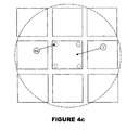
- the corner ejector pins 6a should be kept within a predetermined distance ⁇ from the edges of the die 3. This could include another ejector pin or pins 6 at substantially the center portion of the die 3 as shown in Fig. 4a or 4b or the center ejector pin or pins 6 may be dispensed with, as shown in Fig. 4c.
- the predetermined distance is determinable by considering one or more of the following factors:
- the predetermined distance ⁇ should be iess than a critical vaiue ⁇ c.
- ⁇ c a critical vaiue
- each ejector pin 6, 6a preferably has an effective support area of at least 1 x 10 -4 mm 2 .
- the distribution of a high interfacial peeling stress region concentrates to along the edges and near the corners of the die 3.
- the arrangement of the ejector pins 6a at each corner of the die 3 increases the normal interfacial peeling stress such that it aids the delamination of the interface between the die 3 and the plastic adhesive film 4 - it is easier for the die 3 to be detached from the plastic adhesive film 4 before it cracks.
- the arrangements of the plurality of ejector pins 6a at each corner of the die 3 also reduce the deformation stresses, in particular the bending mode in the die 3 and hence reduce the chance of die crack induced by the die detachment process.
Landscapes
- Container, Conveyance, Adherence, Positioning, Of Wafer (AREA)
- Die Bonding (AREA)
Applications Claiming Priority (2)
| Application Number | Priority Date | Filing Date | Title |
|---|---|---|---|
| US43001002P | 2002-11-27 | 2002-11-27 | |
| US430010P | 2002-11-27 |
Publications (1)
| Publication Number | Publication Date |
|---|---|
| EP1429372A1 true EP1429372A1 (de) | 2004-06-16 |
Family
ID=32326647
Family Applications (1)
| Application Number | Title | Priority Date | Filing Date |
|---|---|---|---|
| EP03078070A Withdrawn EP1429372A1 (de) | 2002-11-27 | 2003-10-01 | Vorrichtung und Verfahren zur Entfernung von dünnschichtigen Halbleiterstrukturen |
Country Status (7)
| Country | Link |
|---|---|
| US (1) | US8026126B2 (de) |
| EP (1) | EP1429372A1 (de) |
| JP (1) | JP2004179627A (de) |
| KR (1) | KR100549359B1 (de) |
| CN (1) | CN100392798C (de) |
| MY (1) | MY143090A (de) |
| TW (1) | TWI221653B (de) |
Cited By (3)
| Publication number | Priority date | Publication date | Assignee | Title |
|---|---|---|---|---|
| EP1793414A1 (de) * | 2005-12-01 | 2007-06-06 | ASM Assembly Automation Ltd. | Eine konfigurierbare Dieabtrennungsvorrichtung |
| SG144767A1 (en) * | 2007-01-23 | 2008-08-28 | Micron Technology Inc | Methods and systems for processing semiconductor workpieces |
| CN101609786B (zh) * | 2008-06-17 | 2011-01-05 | 旺硅科技股份有限公司 | 晶粒取放系统及顶针器 |
Families Citing this family (25)
| Publication number | Priority date | Publication date | Assignee | Title |
|---|---|---|---|---|
| JP4156460B2 (ja) * | 2003-07-09 | 2008-09-24 | Tdk株式会社 | ワークのピックアップ方法及びその装置、実装機 |
| US7303647B2 (en) * | 2004-10-29 | 2007-12-04 | Asm Assembly Automation Ltd. | Driving mechanism for chip detachment apparatus |
| JP4624813B2 (ja) | 2005-01-21 | 2011-02-02 | ルネサスエレクトロニクス株式会社 | 半導体装置の製造方法および半導体製造装置 |
| US8137050B2 (en) * | 2005-09-29 | 2012-03-20 | Semiconductor Energy Laboratory Co., Ltd. | Pickup device and pickup method |
| KR100760300B1 (ko) * | 2006-01-25 | 2007-09-19 | 삼성전자주식회사 | 지지유닛과 이를 갖는 픽업장치 |
| KR100865766B1 (ko) | 2007-07-24 | 2008-10-29 | (주) 에스에스피 | 반도체 다이 이젝팅 장치 |
| KR100889040B1 (ko) | 2007-07-24 | 2009-03-17 | (주) 에스에스피 | 반도체 다이본딩 장비의 플리퍼 |
| WO2009056469A1 (en) * | 2007-10-31 | 2009-05-07 | Oerlikon Assembly Equipment Ag, Steinhausen | Foil perforating needle for detaching a small die from a foil |
| US8141612B2 (en) * | 2009-04-02 | 2012-03-27 | Asm Assembly Automation Ltd | Device for thin die detachment and pick-up |
| US8470130B2 (en) * | 2009-10-20 | 2013-06-25 | Asm Assembly Automation Ltd | Universal die detachment apparatus |
| CN102110747A (zh) * | 2009-12-23 | 2011-06-29 | 永曜光电科技股份有限公司 | 倒装芯片式发光二极管模块的制造方法 |
| DE102011087388A1 (de) * | 2011-02-17 | 2012-08-23 | Semikron Elektronik Gmbh & Co. Kg Ip-Department | Vorrichtung und Verfahren zur Abnahme mindestens eines chipförmigen Halbleiterbauelements von einer Folie |
| US8801352B2 (en) * | 2011-08-11 | 2014-08-12 | International Business Machines Corporation | Pick and place tape release for thin semiconductor dies |
| CN104882401A (zh) * | 2014-02-27 | 2015-09-02 | 联咏科技股份有限公司 | 可重复使用的芯片承载盘及芯片承载与挑拣系统 |
| JP2017531466A (ja) * | 2014-09-24 | 2017-10-26 | ベー・ブラウン・メルズンゲン・アクチエンゲゼルシャフトB.Braun Melsungen Aktiengesellschaft | 安定化用具としてのパッケージング紙の利用 |
| CN108238441A (zh) * | 2016-12-27 | 2018-07-03 | 张家港康得新光电材料有限公司 | 膜片拾取设备 |
| CN109849201A (zh) * | 2017-11-30 | 2019-06-07 | 北京中科镭特电子有限公司 | 一种晶圆劈裂装置及其方法 |
| TWI805564B (zh) | 2018-01-25 | 2023-06-21 | 晶元光電股份有限公司 | 晶粒轉移方法及其裝置 |
| CN114447163B (zh) * | 2018-02-02 | 2024-05-03 | 湖北三安光电有限公司 | 微发光装置的键合治具、键合设备及其键合方法 |
| DE102018125682B4 (de) * | 2018-10-16 | 2023-01-19 | Asm Assembly Systems Gmbh & Co. Kg | Ejektorvorrichtung sowie Verfahren zum Unterstützen eines Ablösens eines auf einer Haltefolie angeordneten elektrischen Bauteils |
| CN113594079B (zh) * | 2020-04-30 | 2024-01-16 | 先进科技新加坡有限公司 | 用于将电子元件从粘性载体分离的顶出器单元 |
| KR102819884B1 (ko) * | 2020-07-20 | 2025-06-12 | 한화세미텍 주식회사 | 다이 박리 장치 및 이를 이용한 다이 박리 방법 |
| CN111770677B (zh) * | 2020-07-24 | 2022-03-11 | 苏州鼎纳自动化技术有限公司 | 一种具有剥料功能的吸取机构 |
| US11889742B2 (en) * | 2020-11-04 | 2024-01-30 | Samsung Display Co., Ltd. | Apparatus of manufacturing display device and method of manufacturing display device |
| JP7655216B2 (ja) * | 2021-12-20 | 2025-04-02 | 三菱電機株式会社 | 半導体製造装置 |
Citations (4)
| Publication number | Priority date | Publication date | Assignee | Title |
|---|---|---|---|---|
| JPS62232935A (ja) * | 1986-04-03 | 1987-10-13 | Mitsubishi Electric Corp | チツプ取り出し装置 |
| EP0431637A1 (de) * | 1989-12-08 | 1991-06-12 | Sumitomo Electric Industries, Ltd. | Aufnahmeverfahren und -apparat für einen chipähnlichen Teil |
| US5589029A (en) * | 1994-07-21 | 1996-12-31 | Matsushita Electric Industrial Co., Ltd. | Semiconductor chip-supply method and apparatus |
| US6201306B1 (en) * | 1995-12-05 | 2001-03-13 | Kabushiki Kaisha Toshiba | Push-up pin of a semiconductor element pushing-up device, and a method for separating |
Family Cites Families (10)
| Publication number | Priority date | Publication date | Assignee | Title |
|---|---|---|---|---|
| US4556362A (en) * | 1983-12-21 | 1985-12-03 | At&T Technologies, Inc. | Methods of and apparatus for handling semiconductor devices |
| US4850780A (en) | 1987-09-28 | 1989-07-25 | Kulicke And Soffa Industries Inc. | Pre-peel die ejector apparatus |
| JP3079502B2 (ja) | 1995-08-18 | 2000-08-21 | 株式会社新川 | ダイ突き上げ装置 |
| JPH11207532A (ja) * | 1998-01-29 | 1999-08-03 | Murata Mfg Co Ltd | 部品供給装置 |
| US6202292B1 (en) * | 1998-08-26 | 2001-03-20 | Micron Technology, Inc. | Apparatus for removing carrier film from a semiconductor die |
| TW451372B (en) * | 1999-06-17 | 2001-08-21 | Shinkawa Kk | Die-holding mechanism, die-packing device and die-bonding device |
| JP2001060611A (ja) * | 1999-06-17 | 2001-03-06 | Shinkawa Ltd | ダイ保持機構、ダイ詰め装置及びダイボンディング装置 |
| JP3719062B2 (ja) * | 1999-09-20 | 2005-11-24 | 松下電器産業株式会社 | 電子部品実装装置 |
| JP2002050670A (ja) * | 2000-08-04 | 2002-02-15 | Toshiba Corp | ピックアップ装置及びピックアップ方法 |
| JP4330821B2 (ja) * | 2001-07-04 | 2009-09-16 | 株式会社東芝 | 半導体装置の製造方法 |
-
2003
- 2003-07-28 US US10/628,503 patent/US8026126B2/en active Active
- 2003-08-15 TW TW092122435A patent/TWI221653B/zh not_active IP Right Cessation
- 2003-09-19 CN CNB031600042A patent/CN100392798C/zh not_active Expired - Lifetime
- 2003-09-24 JP JP2003332274A patent/JP2004179627A/ja active Pending
- 2003-10-01 EP EP03078070A patent/EP1429372A1/de not_active Withdrawn
- 2003-10-06 MY MYPI20033804A patent/MY143090A/en unknown
- 2003-11-19 KR KR1020030082020A patent/KR100549359B1/ko not_active Expired - Lifetime
Patent Citations (4)
| Publication number | Priority date | Publication date | Assignee | Title |
|---|---|---|---|---|
| JPS62232935A (ja) * | 1986-04-03 | 1987-10-13 | Mitsubishi Electric Corp | チツプ取り出し装置 |
| EP0431637A1 (de) * | 1989-12-08 | 1991-06-12 | Sumitomo Electric Industries, Ltd. | Aufnahmeverfahren und -apparat für einen chipähnlichen Teil |
| US5589029A (en) * | 1994-07-21 | 1996-12-31 | Matsushita Electric Industrial Co., Ltd. | Semiconductor chip-supply method and apparatus |
| US6201306B1 (en) * | 1995-12-05 | 2001-03-13 | Kabushiki Kaisha Toshiba | Push-up pin of a semiconductor element pushing-up device, and a method for separating |
Non-Patent Citations (1)
| Title |
|---|
| PATENT ABSTRACTS OF JAPAN vol. 012, no. 101 (E - 595) 2 April 1988 (1988-04-02) * |
Cited By (5)
| Publication number | Priority date | Publication date | Assignee | Title |
|---|---|---|---|---|
| EP1793414A1 (de) * | 2005-12-01 | 2007-06-06 | ASM Assembly Automation Ltd. | Eine konfigurierbare Dieabtrennungsvorrichtung |
| KR100864195B1 (ko) | 2005-12-01 | 2008-10-20 | 에이에스엠 어쌤블리 오토메이션 리미티드 | 형성 가능한 다이 분리 장치 |
| US7470120B2 (en) | 2005-12-01 | 2008-12-30 | Asm Assembly Automation, Ltd. | Configurable die detachment apparatus |
| SG144767A1 (en) * | 2007-01-23 | 2008-08-28 | Micron Technology Inc | Methods and systems for processing semiconductor workpieces |
| CN101609786B (zh) * | 2008-06-17 | 2011-01-05 | 旺硅科技股份有限公司 | 晶粒取放系统及顶针器 |
Also Published As
| Publication number | Publication date |
|---|---|
| US20040115904A1 (en) | 2004-06-17 |
| JP2004179627A (ja) | 2004-06-24 |
| US8026126B2 (en) | 2011-09-27 |
| TW200409272A (en) | 2004-06-01 |
| CN100392798C (zh) | 2008-06-04 |
| KR20040047599A (ko) | 2004-06-05 |
| TWI221653B (en) | 2004-10-01 |
| KR100549359B1 (ko) | 2006-02-08 |
| CN1503320A (zh) | 2004-06-09 |
| MY143090A (en) | 2011-03-15 |
Similar Documents
| Publication | Publication Date | Title |
|---|---|---|
| US8026126B2 (en) | Apparatus and method for thin die detachment | |
| EP1601005A2 (de) | Abziehvorrichtung für Chip-Entnahme | |
| KR101135903B1 (ko) | 박형 다이 분리 및 픽업 장치 | |
| US8470130B2 (en) | Universal die detachment apparatus | |
| TW569355B (en) | Ablation means for adhesive tape, ablation device for adhesive tape, ablation method for adhesive tape, pick-up device for semiconductor chip, pick-up method for semiconductor chips, manufacturing method and device for semiconductor device | |
| US7240422B2 (en) | Apparatus for semiconductor chip detachment | |
| TW451288B (en) | Semiconductor manufacturing apparatus and manufacture of semiconductor device | |
| KR101486104B1 (ko) | 작업물 반송 방법 및 작업물 전달 기구를 갖는 장치 | |
| TWI676226B (zh) | 半導體製造裝置及半導體裝置的製造方法 | |
| JP2005175384A (ja) | 保護テープの貼付方法及び剥離方法 | |
| KR20100127713A (ko) | 웨이퍼 마운트 방법과 웨이퍼 마운트 장치 | |
| JP2001196442A (ja) | ピックアップ装置及びワークのピックアップ方法並びにそのプログラムを格納した記憶媒体 | |
| US20100077590A1 (en) | Die pickup method | |
| US6602736B1 (en) | Method and apparatus for separating semiconductor chips | |
| JP2006237492A (ja) | ウエハ処理装置 | |
| JP2013214683A (ja) | 半導体チップのピックアップ装置 | |
| JP2007158103A (ja) | チップ突き上げ装置 | |
| JP3667241B2 (ja) | ボンディング方法および装置 | |
| JP3409571B2 (ja) | 電子部品の給材容器並びにこれを用いた電子部品の給材方法及び給材装置 | |
| WO2011007398A1 (ja) | ピックアップ装置 | |
| JP2003086540A (ja) | 半導体装置の製造方法及びその製造装置 | |
| CN118645465A (zh) | 半导体制造装置、顶起单元及半导体装置的制造方法 | |
| JPH10209248A (ja) | ダイボンダーにおける突き上げ装置 | |
| KR20090009973U (ko) | 반도체 패키지 제조용 프레임 이송 장치 | |
| JPH01134944A (ja) | 半導体素子のピックアップ方法 |
Legal Events
| Date | Code | Title | Description |
|---|---|---|---|
| PUAI | Public reference made under article 153(3) epc to a published international application that has entered the european phase |
Free format text: ORIGINAL CODE: 0009012 |
|
| AK | Designated contracting states |
Kind code of ref document: A1 Designated state(s): AT BE BG CH CY CZ DE DK EE ES FI FR GB GR HU IE IT LI LU MC NL PT RO SE SI SK TR |
|
| AX | Request for extension of the european patent |
Extension state: AL LT LV MK |
|
| AKX | Designation fees paid | ||
| 17P | Request for examination filed |
Effective date: 20040824 |
|
| RBV | Designated contracting states (corrected) |
Designated state(s): AT CH DE FR GB HU LI |
|
| REG | Reference to a national code |
Ref country code: DE Ref legal event code: 8566 |
|
| RAP1 | Party data changed (applicant data changed or rights of an application transferred) |
Owner name: ASM ASSEMBLY AUTOMATION LTD. |
|
| RIN1 | Information on inventor provided before grant (corrected) |
Inventor name: LEUNG, KA LOK Inventor name: LEE, TAT WING Inventor name: CHONG, CHI MING Inventor name: CHEUNG, YIU MING |
|
| 17Q | First examination report despatched |
Effective date: 20100322 |
|
| STAA | Information on the status of an ep patent application or granted ep patent |
Free format text: STATUS: THE APPLICATION IS DEEMED TO BE WITHDRAWN |
|
| 18D | Application deemed to be withdrawn |
Effective date: 20100803 |