EP1430332B1 - Optische beschichtungen und zugeordnete verfahren - Google Patents
Optische beschichtungen und zugeordnete verfahren Download PDFInfo
- Publication number
- EP1430332B1 EP1430332B1 EP02779285A EP02779285A EP1430332B1 EP 1430332 B1 EP1430332 B1 EP 1430332B1 EP 02779285 A EP02779285 A EP 02779285A EP 02779285 A EP02779285 A EP 02779285A EP 1430332 B1 EP1430332 B1 EP 1430332B1
- Authority
- EP
- European Patent Office
- Prior art keywords
- layer
- reflection layer
- substrate
- additive
- refractive index
- Prior art date
- Legal status (The legal status is an assumption and is not a legal conclusion. Google has not performed a legal analysis and makes no representation as to the accuracy of the status listed.)
- Expired - Lifetime
Links
Images


Classifications
-
- G—PHYSICS
- G02—OPTICS
- G02B—OPTICAL ELEMENTS, SYSTEMS OR APPARATUS
- G02B1/00—Optical elements characterised by the material of which they are made; Optical coatings for optical elements
- G02B1/10—Optical coatings produced by application to, or surface treatment of, optical elements
- G02B1/11—Anti-reflection coatings
-
- G—PHYSICS
- G02—OPTICS
- G02B—OPTICAL ELEMENTS, SYSTEMS OR APPARATUS
- G02B1/00—Optical elements characterised by the material of which they are made; Optical coatings for optical elements
- G02B1/10—Optical coatings produced by application to, or surface treatment of, optical elements
- G02B1/11—Anti-reflection coatings
- G02B1/113—Anti-reflection coatings using inorganic layer materials only
- G02B1/115—Multilayers
- G02B1/116—Multilayers including electrically conducting layers
-
- G—PHYSICS
- G02—OPTICS
- G02B—OPTICAL ELEMENTS, SYSTEMS OR APPARATUS
- G02B5/00—Optical elements other than lenses
- G02B5/20—Filters
- G02B5/208—Filters for use with infrared or ultraviolet radiation, e.g. for separating visible light from infrared and/or ultraviolet radiation
Definitions
- the present invention involves an optical coating for a substrate and a method of manufacturing a coated substrate.
- the optical coating comprises an amorphous material, which includes titanium oxide and one or more oxide additives. Titanium oxide and the additive oxide do not form a solid solution. Since the compounds in the amorphous layer do not form a solid solution, the amorphous layer does not change significantly and remains largely amorphous at the high temperatures used in the heat treatment of a substrate.
- an amorphous film with a high index of refraction is used for a heat treatable optical coating.
- the amorphous film comprises titanium oxide, and at least one additive oxide that raises the crystallization temperature of the titanium oxide. Titanium oxide is preferred since the index of refraction of titanium oxide is high in the visible range, namely 2,45 at 550 nanometers.
- the additive oxide is selected such that titanium oxide and additive oxide are insoluble in each other and, thus, do not form a solid solution. Since the compounds in the amorphous film do not form a solid solution, the amorphous film does not change significantly and remains largely amorphous at the high temperatures used in the heat treatment of a substrate.
- the additive oxide, represented by X is one or more of the oxides of silicon, aluminum, bismuth, gadolinium, tantalum, zinc, and any other additive oxide that is insoluble in titanium oxide.
- the amorphous film is advantageous in any layer of a multi-layer, heat treatable coating.
- the amorphous film does not change significantly its size or its optical properties, such as its index of refraction, at high temperatures. Change in the size of a layer can cause stress-related failure, such as delamination, while a change in the optical properties of a layer can alter the intended design of a coating.
- the amorphous film can reduce or prevent oxidation of the underlying layer from the atmosphere.
- the amorphous film is deposited directly on the substrate, the amorphous film can reduce or prevent haze by slowing the migration of contaminants, such as sodium, in the substrate to any overlying layers. Since the amorphous film has few, if any, grain boundaries, it has a low diffusion coefficient, so diffusion of contaminants across the film is very slow.
- the amorphous film can also reduce or prevent interdiffusion between the two layers surrounding it.
- Visible transmission can be increased by depositing layers of a material with a high-refractive index, such as a refractive index greater than about 2.1, around the metallic layer.
- a higher refractive index material such as a material with a refractive index greater than about 2.1, de-reflects the visible reflection caused by the silver better than a lower refractive index material, such as a material with a refractive index less than about 2.1, does.
- more silver can be used in a low-emissivity coating when a material with a higher index of refraction is used.
- Other materials such as materials without an additive, that remain amorphous to elevated temperatures, do not have a high index of refraction.
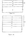
- a multi-layer optical coating 22 includes a first anti-reflection layer 13, a first metallic layer 17, and a second anti-reflection layer 21.
- One or more optional barrier layers 15 and 19 may be present on top of or below the first metallic layer 17, respectively.
- a first barrier layer 15, such as titanium, nickel-chromium, aluminum, or zinc, may be deposited on top of the first anti-reflection layer 13 and below the first metallic layer 17.
- the first barrier layer 15 reduces or prevents the diffusion of contaminants into upper layers.
- a second barrier layer 19, such as titanium, nickel-chromium, aluminum, or zinc, may be deposited on top of the first metallic layer 17 and below the second anti-reflection layer 21.
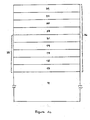
- a multi-layer optical coating 26 includes multi-layer optical coating 22.
- the multi-layer optical coating 26 has a second metallic layer 35, such as silver, over the second anti-reflection layer 21, and a third anti-reflection layer of dielectric 39, such as titanium oxide, tin oxide, zinc oxide, or silicon nitride, over the second metallic layer 35.
- the third anti-reflection layer of dielectric 39 may comprise the amorphous film.
- the deposition of the amorphous material occurs under conditions in which the film has an amorphous (glassy) structure, called a-TiXO.
- the additive oxide represented by XO x is largely insoluble in titanium oxide.
- the dopant oxide does not form a solid solution with titanium oxide.
- the amorphous material may be deposited as a coating for small applications by processes such as sputter, evaporation, sol gel, spray, or any other suitable means, and as a coating for large-scale applications by an energetic process, such as sputter, or any other suitable means.
- Sputtering processes can be any known in the art, such as a process employing rotating cylindrical magnetrons, as described in Lehan et al., U.S. Patent No. 5,814,195, and Wolfe et al., U.S. Patent No. 5,047,131, both of which are expressly incorporated herein in their entireties by this reference, or any other suitable means.
- the specimens were put in a transmission electron microscope ("TEM") with a heating stage.
- TEM transmission electron microscope
- the film with 0% atomic percent of silicon dioxide began nucleation at a temperature of around 300°C, continuing until fully crystallized. Nucleation was evidenced by very small grain size, which indicated the crystallization of the film. There was no growth of grains up to 700°C, but there were many nucleation sites.
- the film with 27% atomic percent of silicon dioxide could be used in applications that have a heat-treatment temperature below its crystallization temperature of about 700°C to about 800°C.
- fritting is performed at about 400°C, heat strengthening at about 600°C, bending at about 650°C, and tempering at about 730°C.
- the atomic percent of silicon dioxide was approximated from the index of refraction of the film.
- the index of refraction was measured optically, as is known in the art.
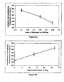
- the crystallization temperature of the film with 0% atomic percent of silicon dioxide was determined to be about 350°C, and the index of refraction was found to be about 2.45.
- the crystallization temperature of the film with 13% atomic percent of silicon dioxide was determined to be about 550°C, and the index of refraction was found to be about 2.35.
- the crystallization temperature of the film with 27% atomic percent of silicon dioxide was determined to be about 700°C to 800°C, and the index of refraction was found to be about 2.2.
- Figure 4a shows that the crystallization temperature increases with a decrease in the index of refraction for Ti-Si-O.
- Figure 4b shows that the crystallization temperature increases with an increase in silicon content for Ti-Si-O.
Landscapes
- Physics & Mathematics (AREA)
- General Physics & Mathematics (AREA)
- Optics & Photonics (AREA)
- Chemical & Material Sciences (AREA)
- Inorganic Chemistry (AREA)
- Health & Medical Sciences (AREA)
- Toxicology (AREA)
- Surface Treatment Of Glass (AREA)
- Laminated Bodies (AREA)
- Surface Treatment Of Optical Elements (AREA)
- Physical Vapour Deposition (AREA)
Claims (16)
- Eine optische Beschichtung für ein Substrat, die Folgendes umfasst:wobei von der ersten Antireflexschicht und der zweiten Antireflexschicht mindestens eine aus einem amorphen Material besteht, das aus Titanoxid und einem Zusatzstoff besteht und dadurch gekennzeichnet ist, dass der Zusatzstoff mit dem Titanoxid keine feste Lösung bildet.eine erste Antireflexschicht aus einem dielektrischen Material;eine erste metallische Schicht über der ersten Antireflexschicht; undeine zweite Antireflexschicht aus einem dielektrischen Material, über der ersten metallischen Schicht;
- Die optische Beschichtung nach Anspruch 1, die Folgendes umfasst:wobei die dritte Antireflexschicht aus einem amorphen Material besteht, welches aus Titanoxid und einem Zusatzstoff besteht, wobei der Zusatzstoff ein Oxid ist, das mit dem Titanoxid keine feste Lösung bildet.eine zweite metallische Schicht über der zweiten Antireflexschicht; undeine dritte Antireflexschicht aus einem dielektrischen Material, über der zweiten metallischen Schicht;
- Die optische Beschichtung nach Anspruch 1 oder 2, wobei der Zusatzstoff aus einer Gruppe ausgewählt wird, die aus Oxiden des Silikons, des Aluminiums, des Wismuts, des Gadoliniums, des Tantals, des Zinks und aus einer beliebigen Kombination dieser Oxide besteht.
- Die optische Beschichtung nach Anspruch 1, wobei die erste oder zweite metallische Schicht aus Silber besteht.
- Die optische Beschichtung nach Anspruch 1 oder 2, die darüber hinaus eine Barriereschicht zwischen der ersten Antireflexschicht und der ersten metallischen Schicht oder zwischen der zweiten Antireflexschicht und der zweiten metallischen Schicht umfasst.
- Die optische Beschichtung nach Anspruch 1 oder 2, die darüber hinaus eine Barriereschicht zwischen der ersten metallischen Schicht und der zweiten AntireBexschieht oder zwischen der zweiten metallischen Schicht und der dritten Antireflexschicht umfasst.
- Die optische Beschichtung nach Anspruch 5 oder 6, wobei die Barriereschicht aus einem Material besteht, das aus einer Gruppe ausgewählt wird, die Titan, Nickelchrom, Aluminium und Zink umfasst.
- Eine optische Beschichtung für ein Substrat, die Folgendes umfasst:wobei von der ersten Schicht mit hohem Brechungsindex und der zweiten Schicht mit hohem Brechungsindex mindestens eine aus einem amorphen Material besteht, welches aus Titanoxid und einem Zusatzstoff besteht und dadurch gekennzeichnet ist, dass der Zusatzstoff ein Oxid ist, das mit dem Titanoxid keine feste Lösung bildet.eine erste Schicht mit hohem Brechungsindex;eine erste Schicht mit niedrigem Brechungsindex, über der ersten Schicht mit hohem Brechungsindex;eine zweite Schicht mit hohem Brechungsindex, über der ersten Schicht mit niedrigem Brechungsindex; undeine zweite Schicht mit niedrigem Brechungsindex, über der zweiten Schicht mit hohem Brechungsindex,
- Die optische Beschichtung nach Anspruch 8, wobei der Zusatzstoff aus einer Gruppe ausgewählt wird, die Oxide des Silikons, des Aluminiums, des Wismuts, des Gadoliniums, des Tantals, des Zinks und eine beliebige Kombination dieser Oxide umfasst.
- Die optische Beschichtung nach Anspruch 9, wobei von der ersten Schicht mit niedrigem Brechungsindex und der zweiten Schicht mit niedrigem Brechungsindex mindestens eine aus einem Material besteht, das aus einer Gruppe ausgewählt wird, die Siliciumdioxid und Silber umfasst.
- Ein Verfahren zum Beschichten von Substraten, das Folgendes umfasst:wobei von der ersten Antireflexschicht und der zweiten Antireflexschicht mindestens eine aus einem amorphen Material besteht, das sich aus Titanoxid und einem Zusatzstoff zusammensetzt und dadurch gekennzeichnet ist, dass der Zusatzstoff ein Oxid ist, dass mit dem Titanoxid keine feste Lösung bildet.das Aufbringen einer ersten Antireflexschicht aus einem dielektrischen Material auf ein Substrat;das Aufbringen einer metallischen Schicht auf die erste Antireflexschicht; unddas Aufbringen einer zweiten Antireflexschicht aus einem dielektrischen Material auf die metallische Schicht;
- Das Verfahren nach Anspruch 11, das darüber hinaus, nach besagtem Aufbringen der ersten Antireflexschicht, der metallischen Schicht und der zweiten Antireflexschicht, das Erhitzen des beschichteten Substrats auf eine Temperatur umfasst, die höher ist als eine Wärmebehandlungstemperatur des Substrats.
- Das Verfahren nach Anspruch 12, wobei von den Verfahren zum Aufbringen der ersten Antireflexschicht, zum Aufbringen der metallischen Schicht und dem Aufbringen der zweiten Antireflexschicht mindestens eines mittels Kathodenzerstäubung erfolgt.
- Das Verfahren nach Anspruch 13, wobei von den Verfahren zum Aufbringen der ersten Antireflexschicht und zum Aufbringen der zweiten Antireflexschicht mindestens eines mittels Kathodenzerstäubung in einer Sauerstoffumgebung erfolgt, und zwar auf ein Target, das aus Titan und dem Zusatzstoff besteht.
- Das Verfahren nach Anspruch 13, wobei von den Verfahren zum Aufbringen der ersten Antireflexschicht und zum Aufbringen der zweiten Antireflexschicht mindestens eines mittels Kathodenzerstäubung in einer Sauerstoffumgebung erfolgt, und zwar auf ein erstes Target, das aus Titan besteht, und auf ein zweites Target, das aus dem Zusatzstoff besteht.
- Das Verfahren nach Anspruch 11, wobei der Zusatzstoff aus einer Gruppe ausgewählt wird, die Oxide des Silikons, des Aluminiums, des Wismuts, des Gadoliniums, des Tantals, des Zinks und eine beliebige Kombination davon umfasst.
Applications Claiming Priority (3)
| Application Number | Priority Date | Filing Date | Title |
|---|---|---|---|
| US09/944,050 US20030043464A1 (en) | 2001-08-30 | 2001-08-30 | Optical coatings and associated methods |
| US944050 | 2001-08-30 | ||
| PCT/EP2002/009688 WO2003021304A1 (en) | 2001-08-30 | 2002-08-30 | Optical coatings and associated methods |
Publications (2)
| Publication Number | Publication Date |
|---|---|
| EP1430332A1 EP1430332A1 (de) | 2004-06-23 |
| EP1430332B1 true EP1430332B1 (de) | 2005-11-16 |
Family
ID=25480702
Family Applications (1)
| Application Number | Title | Priority Date | Filing Date |
|---|---|---|---|
| EP02779285A Expired - Lifetime EP1430332B1 (de) | 2001-08-30 | 2002-08-30 | Optische beschichtungen und zugeordnete verfahren |
Country Status (7)
| Country | Link |
|---|---|
| US (1) | US20030043464A1 (de) |
| EP (1) | EP1430332B1 (de) |
| JP (1) | JP2005502076A (de) |
| KR (1) | KR20040044524A (de) |
| CN (1) | CN100406917C (de) |
| AT (1) | ATE310251T1 (de) |
| WO (1) | WO2003021304A1 (de) |
Families Citing this family (25)
| Publication number | Priority date | Publication date | Assignee | Title |
|---|---|---|---|---|
| JP4174216B2 (ja) * | 2002-01-18 | 2008-10-29 | フジノン株式会社 | バリア層を有する光学素子、光学系および投映プロジェクタ装置 |
| US7294404B2 (en) * | 2003-12-22 | 2007-11-13 | Cardinal Cg Company | Graded photocatalytic coatings |
| ATE377580T1 (de) * | 2004-07-12 | 2007-11-15 | Cardinal Cg Co | Wartungsarme beschichtungen |
| JP5301833B2 (ja) * | 2004-10-04 | 2013-09-25 | カーディナル・シージー・カンパニー | 薄膜コーティング及び仮保護技術、断熱板ガラスユニット、並びに関連方法 |
| US7923114B2 (en) * | 2004-12-03 | 2011-04-12 | Cardinal Cg Company | Hydrophilic coatings, methods for depositing hydrophilic coatings, and improved deposition technology for thin films |
| US8092660B2 (en) * | 2004-12-03 | 2012-01-10 | Cardinal Cg Company | Methods and equipment for depositing hydrophilic coatings, and deposition technologies for thin films |
| US7371599B2 (en) * | 2006-04-17 | 2008-05-13 | United Microeletronics Corp. | Image sensor and method of forming the same |
| US20070256934A1 (en) * | 2006-05-08 | 2007-11-08 | Perata Michael R | Apparatus and Method for Coating Substrates With Approximate Process Isolation |
| US20080011599A1 (en) | 2006-07-12 | 2008-01-17 | Brabender Dennis M | Sputtering apparatus including novel target mounting and/or control |
| WO2008081837A1 (ja) * | 2006-12-27 | 2008-07-10 | Asahi Glass Company, Limited | 反射防止体およびディスプレイ装置 |
| US7807248B2 (en) * | 2007-08-14 | 2010-10-05 | Cardinal Cg Company | Solar control low-emissivity coatings |
| CA2664369A1 (en) | 2007-09-14 | 2009-03-19 | Cardinal Cg Company | Low-maintenance coatings, and methods for producing low-maintenance coatings |
| KR100984701B1 (ko) * | 2008-08-01 | 2010-10-01 | 엘지전자 주식회사 | 태양 전지의 제조 방법 |
| US20100180939A1 (en) * | 2009-01-22 | 2010-07-22 | Sharma Pramod K | Heat treatable magnesium fluoride inclusive coatings, coated articles including heat treatable magnesium fluoride inclusive coatings, and methods of making the same |
| EP2230539B1 (de) * | 2009-03-19 | 2019-12-04 | Viavi Solutions Inc. | Ausformung einer Abstandsschicht in einem Interferenzfilter |
| CN101932211B (zh) * | 2009-06-25 | 2013-04-24 | 深圳富泰宏精密工业有限公司 | 视窗及应用该视窗的电子装置 |
| US9206078B2 (en) * | 2013-03-13 | 2015-12-08 | Intermolecular, Inc. | Barrier layers for silver reflective coatings and HPC workflows for rapid screening of materials for such barrier layers |
| JP6282142B2 (ja) * | 2014-03-03 | 2018-02-21 | 日東電工株式会社 | 赤外線反射基板およびその製造方法 |
| US10604442B2 (en) | 2016-11-17 | 2020-03-31 | Cardinal Cg Company | Static-dissipative coating technology |
| CN111699430B (zh) * | 2018-01-29 | 2022-07-22 | 应用材料公司 | 用于光学器件增强的润湿层 |
| WO2020129456A1 (ja) * | 2018-12-19 | 2020-06-25 | 富士フイルム株式会社 | 光触媒複合材、並びに、サイネージ用ディスプレイ保護部材、タッチパネル用保護部材、太陽電池用保護部材、センサカバー用保護部材、サイネージ用ディスプレイ、タッチパネル、太陽電池、及び、センサカバー |
| WO2022020077A1 (en) * | 2020-07-22 | 2022-01-27 | Applied Materials, Inc. | Doped amorphous optical device films and deposition via incorporation of dopant atoms |
| US20220260766A1 (en) * | 2021-02-17 | 2022-08-18 | Applied Materials, Inc. | Optical device film with tunable refractive index |
| TW202300959A (zh) * | 2021-03-11 | 2023-01-01 | 美商應用材料股份有限公司 | 藉由物理氣相沉積所沉積的氧化鈦光學裝置薄膜 |
| CN115347454A (zh) * | 2021-05-13 | 2022-11-15 | 中芯国际集成电路制造(上海)有限公司 | 光学器件的结构及光学器件的形成方法 |
Family Cites Families (13)
| Publication number | Priority date | Publication date | Assignee | Title |
|---|---|---|---|---|
| JPS58202408A (ja) * | 1982-05-20 | 1983-11-25 | Nippon Soken Inc | 熱線反射膜 |
| US5318685A (en) * | 1987-08-18 | 1994-06-07 | Cardinal Ig Company | Method of making metal oxide films having barrier properties |
| US5264286A (en) * | 1988-03-03 | 1993-11-23 | Asahi Glass Company Ltd. | Laminated glass structure |
| EP0486475B1 (de) * | 1988-03-03 | 1997-12-03 | Asahi Glass Company Ltd. | Amorpher Oxid-Film und Gegenstand mit einem solchen Film |
| US5344718A (en) * | 1992-04-30 | 1994-09-06 | Guardian Industries Corp. | High performance, durable, low-E glass |
| DK0758306T3 (da) * | 1994-05-03 | 1999-05-10 | Cardinal Ig Co | Transparent genstand med beskyttelsesfilm af siliciumnitrid |
| US5830252A (en) * | 1994-10-04 | 1998-11-03 | Ppg Industries, Inc. | Alkali metal diffusion barrier layer |
| US5821001A (en) * | 1996-04-25 | 1998-10-13 | Ppg Industries, Inc. | Coated articles |
| JPH10237352A (ja) * | 1997-02-24 | 1998-09-08 | Tao:Kk | 多機能コーティング剤 |
| EP0963960A1 (de) * | 1998-06-08 | 1999-12-15 | Glaverbel | Durchsichtiges Substrat mit Silberbeschichtung |
| JP3290629B2 (ja) * | 1998-06-22 | 2002-06-10 | アルプス電気株式会社 | 光学多層膜フィルタ |
| JP2001025666A (ja) * | 1999-07-14 | 2001-01-30 | Nippon Sheet Glass Co Ltd | 積層体およびその製造方法 |
| US6475626B1 (en) * | 1999-12-06 | 2002-11-05 | Guardian Industries Corp. | Low-E matchable coated articles and methods of making same |
-
2001
- 2001-08-30 US US09/944,050 patent/US20030043464A1/en not_active Abandoned
-
2002
- 2002-08-30 CN CN028170245A patent/CN100406917C/zh not_active Expired - Fee Related
- 2002-08-30 KR KR10-2004-7003117A patent/KR20040044524A/ko not_active Withdrawn
- 2002-08-30 AT AT02779285T patent/ATE310251T1/de not_active IP Right Cessation
- 2002-08-30 JP JP2003525333A patent/JP2005502076A/ja not_active Withdrawn
- 2002-08-30 WO PCT/EP2002/009688 patent/WO2003021304A1/en not_active Ceased
- 2002-08-30 EP EP02779285A patent/EP1430332B1/de not_active Expired - Lifetime
Also Published As
| Publication number | Publication date |
|---|---|
| CN100406917C (zh) | 2008-07-30 |
| JP2005502076A (ja) | 2005-01-20 |
| WO2003021304A1 (en) | 2003-03-13 |
| CN1549935A (zh) | 2004-11-24 |
| ATE310251T1 (de) | 2005-12-15 |
| KR20040044524A (ko) | 2004-05-28 |
| EP1430332A1 (de) | 2004-06-23 |
| US20030043464A1 (en) | 2003-03-06 |
Similar Documents
| Publication | Publication Date | Title |
|---|---|---|
| US20030043464A1 (en) | Optical coatings and associated methods | |
| EP1851354B2 (de) | Verfahren zur herstellung einer low-e-beschichtung unter verwendung eines zinkhaltigen keramiktargets und dabei verwendetes target | |
| US7632572B2 (en) | Double silver low-emissivity and solar control coatings | |
| CN1747907B (zh) | 载有涂层叠层的玻璃板 | |
| JP2625079B2 (ja) | 放射率の低い太陽熱制御型耐久性薄膜コーティング | |
| EP3004015B1 (de) | Verglasung mit geringer emissivität | |
| US20070029186A1 (en) | Method of thermally tempering coated article with transparent conductive oxide (TCO) coating using inorganic protective layer during tempering and product made using same | |
| EP1140723B1 (de) | Verbesserungen im beschichten von glass | |
| CZ299337B6 (cs) | Zpusob vytvárení povlaku na skle magnetronovým naprašováním, sklenený tabulovitý dílec s transparentním tenkovrstvým systémem, a dvojsklo obsahující takový dílec | |
| EP3004014A2 (de) | Emissionsarme sonnenschutzverglasung | |
| EP2173677A1 (de) | Wärmebehandelbare beschichtete glasscheibe | |
| EP4139258A1 (de) | Sonnenschutzverglasung und verfahren zu deren herstellung | |
| EP4139261A1 (de) | Verglasung mit geringer emissivität und verfahren zu ihrer herstellung | |
| JP2018514499A (ja) | 低放射率コーティング用のチタンニッケルニオブ合金バリア | |
| US9296651B2 (en) | Heat stable SnAl and SnMg based dielectrics | |
| US10604834B2 (en) | Titanium nickel niobium alloy barrier for low-emissivity coatings | |
| WO2021214108A1 (en) | Low-emissivity glazing and method of its production | |
| WO2021019259A1 (en) | Coated substrate | |
| JPH0255246A (ja) | 高耐久性熱線遮へいガラスおよびその製造方法 | |
| WO2025186542A1 (en) | Coated glass pane | |
| JPH0597476A (ja) | 熱処理可能な断熱ガラスおよびその製法 |
Legal Events
| Date | Code | Title | Description |
|---|---|---|---|
| PUAI | Public reference made under article 153(3) epc to a published international application that has entered the european phase |
Free format text: ORIGINAL CODE: 0009012 |
|
| 17P | Request for examination filed |
Effective date: 20040326 |
|
| AK | Designated contracting states |
Kind code of ref document: A1 Designated state(s): AT BE BG CH CY CZ DE DK EE ES FI FR GB GR IE IT LI LU MC NL PT SE SK TR |
|
| AX | Request for extension of the european patent |
Extension state: AL LT LV MK RO SI |
|
| 17Q | First examination report despatched |
Effective date: 20041206 |
|
| GRAP | Despatch of communication of intention to grant a patent |
Free format text: ORIGINAL CODE: EPIDOSNIGR1 |
|
| REG | Reference to a national code |
Ref country code: DE Ref legal event code: 8566 |
|
| RBV | Designated contracting states (corrected) |
Designated state(s): AT BE CH LI LU NL |
|
| GRAS | Grant fee paid |
Free format text: ORIGINAL CODE: EPIDOSNIGR3 |
|
| GRAA | (expected) grant |
Free format text: ORIGINAL CODE: 0009210 |
|
| AK | Designated contracting states |
Kind code of ref document: B1 Designated state(s): AT BE CH LI LU NL |
|
| PG25 | Lapsed in a contracting state [announced via postgrant information from national office to epo] |
Ref country code: NL Free format text: LAPSE BECAUSE OF FAILURE TO SUBMIT A TRANSLATION OF THE DESCRIPTION OR TO PAY THE FEE WITHIN THE PRESCRIBED TIME-LIMIT Effective date: 20051116 Ref country code: AT Free format text: LAPSE BECAUSE OF FAILURE TO SUBMIT A TRANSLATION OF THE DESCRIPTION OR TO PAY THE FEE WITHIN THE PRESCRIBED TIME-LIMIT Effective date: 20051116 |
|
| REG | Reference to a national code |
Ref country code: CH Ref legal event code: EP |
|
| REG | Reference to a national code |
Ref country code: CH Ref legal event code: NV Representative=s name: BOVARD AG PATENTANWAELTE |
|
| NLV1 | Nl: lapsed or annulled due to failure to fulfill the requirements of art. 29p and 29m of the patents act | ||
| PGFP | Annual fee paid to national office [announced via postgrant information from national office to epo] |
Ref country code: BE Payment date: 20060828 Year of fee payment: 5 |
|
| PGFP | Annual fee paid to national office [announced via postgrant information from national office to epo] |
Ref country code: LU Payment date: 20060829 Year of fee payment: 5 Ref country code: CH Payment date: 20060829 Year of fee payment: 5 |
|
| PLBE | No opposition filed within time limit |
Free format text: ORIGINAL CODE: 0009261 |
|
| STAA | Information on the status of an ep patent application or granted ep patent |
Free format text: STATUS: NO OPPOSITION FILED WITHIN TIME LIMIT |
|
| 26N | No opposition filed |
Effective date: 20060817 |
|
| BERE | Be: lapsed |
Owner name: *VON ARDENNE ANLAGENTECHNIK G.M.B.H. Effective date: 20070831 |
|
| REG | Reference to a national code |
Ref country code: CH Ref legal event code: PL |
|
| PG25 | Lapsed in a contracting state [announced via postgrant information from national office to epo] |
Ref country code: LI Free format text: LAPSE BECAUSE OF NON-PAYMENT OF DUE FEES Effective date: 20070831 Ref country code: CH Free format text: LAPSE BECAUSE OF NON-PAYMENT OF DUE FEES Effective date: 20070831 |
|
| PG25 | Lapsed in a contracting state [announced via postgrant information from national office to epo] |
Ref country code: BE Free format text: LAPSE BECAUSE OF NON-PAYMENT OF DUE FEES Effective date: 20070831 |
|
| PG25 | Lapsed in a contracting state [announced via postgrant information from national office to epo] |
Ref country code: LU Free format text: LAPSE BECAUSE OF NON-PAYMENT OF DUE FEES Effective date: 20070830 |