EP1430504B1 - Verfahren zur herstellung einer matrix für kathodenstrahlröhre - Google Patents
Verfahren zur herstellung einer matrix für kathodenstrahlröhre Download PDFInfo
- Publication number
- EP1430504B1 EP1430504B1 EP02780310A EP02780310A EP1430504B1 EP 1430504 B1 EP1430504 B1 EP 1430504B1 EP 02780310 A EP02780310 A EP 02780310A EP 02780310 A EP02780310 A EP 02780310A EP 1430504 B1 EP1430504 B1 EP 1430504B1
- Authority
- EP
- European Patent Office
- Prior art keywords
- light
- faceplate panel
- photoresist
- layer
- source position
- Prior art date
- Legal status (The legal status is an assumption and is not a legal conclusion. Google has not performed a legal analysis and makes no representation as to the accuracy of the status listed.)
- Expired - Lifetime
Links
Images




Classifications
-
- H—ELECTRICITY
- H01—ELECTRIC ELEMENTS
- H01J—ELECTRIC DISCHARGE TUBES OR DISCHARGE LAMPS
- H01J9/00—Apparatus or processes specially adapted for the manufacture, installation, removal, maintenance of electric discharge tubes, discharge lamps, or parts thereof; Recovery of material from discharge tubes or lamps
- H01J9/20—Manufacture of screens on or from which an image or pattern is formed, picked up, converted or stored; Applying coatings to the vessel
- H01J9/22—Applying luminescent coatings
- H01J9/227—Applying luminescent coatings with luminescent material discontinuously arranged, e.g. in dots or lines
-
- H—ELECTRICITY
- H01—ELECTRIC ELEMENTS
- H01J—ELECTRIC DISCHARGE TUBES OR DISCHARGE LAMPS
- H01J29/00—Details of cathode-ray tubes or of electron-beam tubes of the types covered by group H01J31/00
- H01J29/02—Electrodes; Screens; Mounting, supporting, spacing or insulating thereof
- H01J29/10—Screens on or from which an image or pattern is formed, picked up, converted or stored
- H01J29/18—Luminescent screens
- H01J29/30—Luminescent screens with luminescent material discontinuously arranged, e.g. in dots, in lines
- H01J29/32—Luminescent screens with luminescent material discontinuously arranged, e.g. in dots, in lines with adjacent dots or lines of different luminescent material, e.g. for colour television
- H01J29/327—Black matrix materials
-
- H—ELECTRICITY
- H01—ELECTRIC ELEMENTS
- H01J—ELECTRIC DISCHARGE TUBES OR DISCHARGE LAMPS
- H01J9/00—Apparatus or processes specially adapted for the manufacture, installation, removal, maintenance of electric discharge tubes, discharge lamps, or parts thereof; Recovery of material from discharge tubes or lamps
- H01J9/20—Manufacture of screens on or from which an image or pattern is formed, picked up, converted or stored; Applying coatings to the vessel
- H01J9/22—Applying luminescent coatings
- H01J9/227—Applying luminescent coatings with luminescent material discontinuously arranged, e.g. in dots or lines
- H01J9/2278—Application of light absorbing material, e.g. between the luminescent areas
Definitions
- the invention relates to a color cathode-ray tube (CRT) and, more particularly to a color CRT including a luminescent screen assembly.
- CRT color cathode-ray tube
- a color cathode-ray tube typically includes an electron gun, an aperture mask, and a screen.
- the aperture mask is interposed between the electron gun and the screen.
- the screen is located on an inner surface of a faceplate of the CRT tube.
- the aperture mask functions to direct electron beams generated in the electron gun toward appropriate color-emitting phosphors on the screen of the CRT tube.
- the screen may be a luminescent screen.
- Luminescent screens typically comprise an array of three different color-emitting phosphors (e. g., green, blue, and red). Each color-emitting phosphor is separated one from the other by a matrix line.
- the matrix lines are formed of a light-absorbing black inert material.
- the matrix lines may be deposited on the screen using aperture mask photolithographic processes, such as those described in U. S. Patent No. 3,558,310.
- aperture mask photolithographic processes images of the aperture mask are formed in a layer of photoresist material coated on the screen, through exposure to actinic ultraviolet (UV) light and development in an appropriate developer, providing covered areas and uncovered areas on the screen surface.
- UV light actinic ultraviolet
- the covered areas on the screen surface are exposed to greater dosages of the actinic UV light, while the uncovered areas on the screen surface are exposed to lesser dosages of the actinic UV light.
- the aperture mask is positioned a fixed distance from the screen such that shadows therefrom, projected onto the resist coated screen during exposure to actinic UV light, uncover matrix line openings in the photoresist having desired dimensions and positioned at appropriate locations on the screen.
- the covered areas define the matrix line openings, which will be filled with phosphor material.
- the uncovered areas define the black, light absorbing matrix lines.
- the matrix lines are formed by depositing the matrix material on both the covered and uncovered areas of the screen surface. After the matrix material, which typically comprises colloidal graphite, dries, an etchant is applied to solubilize the remaining photoresist that had been exposed to greater dosages of actinic UV light.
- the matrix line structure is completed by developing with high-pressure water such that the remaining photoresist and the matrix material coating it are released, thereby leaving behind on the surface of the screen only the matrix material that had coated the uncovered areas thereof.
- aperture masks typically have a transmission of about 18 % to about 22 %. Recently, in order to increase the brightness in a CRT tube without increasing the respective size of the matrix openings, aperture masks having transmissions of about 20 % to about 80 % have been incorporated into the color CRT tube. However, matrix line formation using aperture masks with transmissions of about 30 % to about 80 % cannot be achieved utilizing conventional matrix processes such as those described in U. S. Patent No. 3,558,310, since the light images projected therefrom overlap each other causing the location of such matrix lines to be misaligned on the screen surface as well as have varying dimensions.
- the present invention as claimed relates to a method of manufacturing a luminescent screen assembly, having a light-absorbing matrix with a plurality of substantially equally-sized openings therein, on an inner surface of a faceplate panel of a cathode-ray tube (CRT).
- the tube has a color selection electrode or aperture mask spaced from the inner surface of the faceplate panel in which the color selection electrode has a plurality of slots.
- the method as claimed includes the steps of exposing a first photoresist layer to light from a light source, located relative to a central source position, as well as two symmetrical source positions relative to the central source position.
- the exposure selectively alters the solubility of the illuminated areas of the first photoresist layer to produce therein regions with greater solubility and regions of lesser solubility.
- the regions of greater solubility are subsequently removed to uncover areas of the inner surface of the faceplate panel, while retaining the regions of lesser solubility.
- the inner surface of the faceplate panel and the retained regions are then overcoated with a light-absorbing material.
- the retained regions of the first photoresist layer and the light-absorbing material thereon are removed, uncovering portions of the faceplate panel and defining first guardbands of light-absorbing material on the inner surface of the faceplate panel.
- This photolithographic process is repeated with a second photoresist layer and a third photoresist layer to define second guardbands of light-absorbing material and third guardbands of light-absorbing material, respectively.
- the light source positions for the second photoresist layer and the third photoresist layer are located at asymmetric positions relative to the central source position.
- the light-absorbing material applied to the interior surface of the faceplate panel preferably includes greater than about 5 % by weight of solids. Additionally, an overcoat layer may be applied over the light absorbing material to seal such layer and reduce the porosity thereof.
- FIG. 1 shows a color cathode-ray tube (CRT) 10 having a glass envelope 11 comprising a faceplate panel 12 and a tubular neck 14 connected by a funnel 15.
- the funnel 15 has an internal conductive coating (not shown) that is in contact with, and extends from, an anode button 16 to the neck 14.
- the faceplate panel 12 comprises a viewing faceplate 18 and a peripheral flange or sidewall 20 that is sealed to the funnel 15 by a glass frit 21.
- a three-color luminescent phosphor screen 22 is carried on the inner surface of the viewing faceplate 18.
- the screen 22, shown in cross-section in FIG. 2, is a line screen which includes a multiplicity of screen elements comprising red-emitting, green-emitting, and blue-emitting phosphor stripes R, G, and B, respectively, arranged in triads, each triad including a phosphor line of each of the three colors.
- the R, G, B, phosphor stripes are generally printed with a vertical orientation.
- a thin conductive layer (not shown), overlies the screen 22 and provides means for applying a uniform first anode potential to the screen 22, as well as for reflecting light, emitted from the phosphor elements, through the faceplate 18.
- the screen 22 and the overlying aluminum layer comprise a screen assembly.
- a multi-aperture color selection electrode, or mask 25 is removably mounted, by conventional means, within the faceplate panel 12, in predetermined spaced relation to the screen 22. This space relation or distance of the mask 25 from the faceplate panel 12 is referred to as the "Q" spacing.
- An electron gun 26 shown schematically by the dashed lines in FIG. 1, is centrally mounted within the neck 14, to generate and direct three inline electron beams 28, a center and two side or outer beams, along convergent paths through the mask 25 to the screen 22.
- the inline direction of the center beam 28 is approximately normal to the plane of the paper.
- the CRT 10 of FIG. 1 is designed to be used with an external magnetic deflection yoke 30, in the neighborhood of the funnel-to-neck junction.
- the yoke 30 subjects the three electron beams 28 to magnetic fields that cause the electron beams 28 to scan a horizontal and vertical rectangular raster across the screen 22.
- the mask 25 is formed, preferably, from a thin rectangular sheet of about 0.05 mm (2 mil) thick low carbon steel, that includes two horizontal sides and two vertical sides.
- the two horizontal sides of the mask 25 parallel the central major axis, X, of the mask and the two vertical sides parallel the central minor axis, Y, of the mask.
- the mask 25 includes an apertured portion that contains a plurality of elongated strands 32 separated by slots 33 that parallel the minor axis, Y, of the mask.
- the mask pitch, D m defined as the transverse dimension of a strand 32 and an adjacent slot 33, is 0.87 mm (37 mils).
- each strand 32 can have a transverse dimension, or width, w, of about 0.38 mm (15 mils) and each slot 33 can have a width, a', of about 0.53 mm (21 mils).
- the slots 33 extend from one horizontal side of the mask to the other horizontal side thereof.
- the pitch, D m of the mask 25 can be varied.
- each matrix opening has a width, c, of about 0.13 mm (5 mils).
- the screen 22, formed on the viewing faceplate 18, includes the light-absorbing matrix 23 with rectangular openings in which the color-emitting phosphor lines are disposed.
- the corresponding matrix openings have a width, c, of about 0.20 mm (8 mils).
- the width, d, of each matrix line is about 0.10 mm (4 mils) and each phosphor triad has a width or screen pitch, T, of about 0.96 mm (38 mils).
- the mask 25 is spaced at a distance, Q, (hereinafter Q-spacing) of about 15.24 mm (600 mils) from the center of the interior surface of the faceplate panel 12.
- the process for manufacturing the light-absorbing matrix begins with cleaning the interior surface of the faceplate 18 with an acid such as hydrofluoric acid (HF).
- HF hydrofluoric acid
- a polymer precoat layer (not shown) may be applied to the interior surface of the faceplate 18, as indicated by step 52 in FIG. 4a.
- the polymer precoat layer is a thin film that enhances the adhesion of the light absorbing material and promotes greater opacity of the matrix lines.
- the polymer precoat layer may comprise a material such as polyvinyl alcohol (PVA).
- PVA polyvinyl alcohol
- the polymer precoat layer may be deposited by spin coating a 0.1 to 0.3 % aqueous PVA solution thereon.
- the polymer precoat layer typically has a thickness no greater than about 0.25 ⁇ m.
- a first photoresist layer 56 is applied, by spin coating, on the inner surface of the viewing faceplate 18.
- the first photoresist layer 56 may comprise a polyvinyl pyrrolidone (PVP)-diazido stilbene system, a polyvinyl alcohol (PVA)-dichromate system, or other suitable negative photoresist systems.
- a mask 25 is secured near the faceplate panel 12 and the panel-mask assembly placed on a lighthouse (not shown).
- the mask 25 is positioned between the faceplate panel 12 and a movable light source 51, shown in FIG. 6.
- the first photoresist layer 56 is exposed to light, through the slots 33 of the mask 25, from the RB source positions (green source positions), as indicated by step 78 in FIG. 4a.
- the first color source position, +G is located at a distance, ⁇ X, relative to a central source position or standard green location, 0.
- the second color source position, -G is located a distance, - ⁇ X, relative to the central source position, 0.
- ⁇ X can be about 1.78 mm (70 mils).
- the third source position is preferably the central source position, 0. However, this third source position can be from at least one position between - ⁇ X and ⁇ X The third source position ensures that regions 53 of the first photoresist layer 56 are entirely exposed thereby producing a desired level of lesser solubility therein.
- the Q-spacing between the mask 25 and the interior surface of the faceplate panel 12, on which the first photoresist layer 56 is disposed is about 449 mils (11,4 mm).
- the light emanating from the three source positions selectively alters the solubility of the illuminated areas of the first photoresist layer 56 thereby producing regions 53 of lesser solubility.
- the areas 54 define the matrix RB guardband where +G defines the red edge of guardband RB and -G defines the blue edge of guardband RB. Area 54a defines where the phosphor screen terminates.
- the first photoresist layer 56 is developed by rinsing the panel 12 with a suitable solvent, such as for example water. This development step removes the regions 54 and 54a of greater solubility, thereby exposing areas 57 of the surface of the panel 12, while leaving intact the illuminated areas 53 of layer 56 having lesser solubility.
- a suitable solvent such as for example water.
- the matrix is formed, as shown in FIG. 5d and indicated in step 88 of FIG. 4a, by overcoating the exposed areas 57 of the surface of the panel 12 as well as the retained areas 53 of layer 56, having lesser solubility, with a first layer of light absorbing material 59.
- the first layer of the light absorbing material 59 adheres to the interior surface of the faceplate panel 12 in the uncovered areas 57 and 57a.
- the first layer of the light-absorbing material 59 is preferably made of a suitable graphite composition such as those commercially available from Acheson Colloids Company, Port Huron, Michigan.
- the first layer of the light-absorbing material 59 preferably comprises a suspension of sub-micron graphite colloids. Additionally, the first layer of light-absorbing material may also include surface-active agents. It is believed that the surface-active agents in the light-absorbing material layer promotes improved wetting of the faceplate panel 12 for film-formation thereon.
- the graphite colloids in the suspension are optionally coated with an oxidation barrier.
- Suitable oxidation barriers may comprise oxides such as, for example, silicon dioxide (SiO 2 ), and aluminum oxide (Al 2 O 3 ). The oxidation barrier is believed to reduce the oxidation of the graphite during subsequent tube processing.
- a composition containing the light-absorbing material with a solids concentration between about 5.5 % and about 8.0 % is applied to the uncovered areas 57 and 57a, as well as the retained areas 53 of lesser solubility.
- the first layer of light-absorbing material is dried at temperatures within a range of about 40 °C to about 70 °C for a time period of about 3 minutes to about 5 minutes.
- the thickness of the first layer of light absorbing material is about 1 ⁇ m.
- the light-absorbing matrix is developed by depositing a suitable solvent, such as aqueous periodic acid, or the equivalent, onto the matrix to soften and swell the underlying retained areas 53 of layer 56 having lesser solubility.
- a suitable solvent such as aqueous periodic acid, or the equivalent
- the matrix is then flushed with water to remove the loosened, less soluble, retained areas 53 of layer 56, forming openings therein, but leaving the RB guardbands and a border 62 of light-absorbing material attached to the exposed portions of the interior surface of the faceplate panel 12.
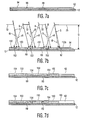
- a second photoresist layer 94 is applied on the interior surface of the faceplate panel 12, as shown in FIG. 7a and indicated in step 95 of FIG. 4b.
- the second photoresist layer 94 is exposed to light, through the mask 25, from the GR source positions 51, within a lighthouse (not shown).
- the color first source position, +B is asymmetrically located a distance, 2X- ⁇ X, about 8.99 mm (354 mils) relative to the central source position, 0.
- the position -X and 2X are known as the primary and secondary source positions for blue, respectively.
- the second color source position, -B is asymmetrically located a distance, -X+ ⁇ X, about -3.61 mm (-142 mils), relative to a central source position, 0.
- the third position is the primary source position for blue, -X, -212 mils (or otherwise known as the standard blue position used in printing blue phosphors lines in a screening process and printing the blue matrix opening in a conventional matrix process.
- this third source position can be from at least one position between -X- ⁇ X and -X+ ⁇ X.
- the Q-spacing between the mask 25 and the inner surface of the faceplate panel 12 is about 449 mils.
- the light emanating from the GR source positions selectively alters the solubility of the illuminate areas of the second photoresist layer 94, thereby producing regions 150 of lesser solubility.
- the areas of the second photoresist layer 94 that are shaded by the mask strands 32 are unchanged and constitute regions 152 and 152a of greater solubility.
- the photoresist is developed with water, removing regions 152 of greater solubility and uncovering areas 154 of the inner surface of the faceplate panel 12. Regions 150 of the second photoresist layer 94 with lesser solubility are retained.
- the matrix is formed, as shown in FIG. 7d and indicated in step 100 of FIG. 4b, by overcoating the uncovered areas 154 and the retained regions 150 of lesser solubility on the inner surface of the faceplate panel 12 with a second layer of light-absorbing material 156.
- the second layer of light-absorbing material 156 preferably has a similar composition, thickness, etc, as the first layer of light-absorbing material 59 and may be applied using a similar process.
- the second layer of the light-absorbing material 156 is dried, as indicated in step 102 of FIG. 4b, and retained regions 150 of the second photoresist layer 94 as well as the second layer of light-absorbing material 156 thereon, are removed.
- the retained regions 150 of the second photoresist layer 94 are removed by rinsing the faceplate panel 12 using a suitable solvent, such as aqueous periodic acid, or the equivalent.
- a suitable solvent such as aqueous periodic acid, or the equivalent.
- the process is repeated for a third time when a third layer of photoresist material 210 is provided on the inner surface of the faceplate panel 12, as shown in FIG. 9a and indicated in step 200 of FIG. 4c.
- the third photoresist layer 210 is exposed to light, through the mask 25, from the GB source positions, within a lighthouse (not shown).
- the first color source position, +R is asymmetrically located a distance, X- ⁇ X, about 3.61 mm (142 mils) relative to the central source position, 0.
- the second color source position, -R is asymmetrically located a distance, -2X+ ⁇ X, about -8.99 mm (-354 mils), relative to a central source position, 0.
- the position X and -2X is also known as the primary and secondary source positions for red, respectively.
- the third source position is the primary source position red, X, 212 mils (5,38 mm) (or otherwise known as the standard red position used in printing blue phosphors lines in a screening process and printing the blue matrix opening in a conventional matrix process).
- this third source position can be from at least one position between X- ⁇ X and X+ ⁇ X.
- the Q-spacing between the mask 25 and the inner surface of the faceplate panel 12, on which the third photoresist layer 210 is disposed remains at about 449 mils (11,4 mm).
- the light emanating from the GB source positions selectively alters the solubility of the illuminated areas of the third photoresist layer 210, thereby producing regions 506 of lesser solubility.
- the areas of the third photoresist layer 210 that are shaded by the mask strands 32 are unchanged and constitute regions 508 and 508a of greater solubility.
- the third photoresist layer 210 is developed with water, thereby removing the regions of greater solubility 508 and 508a, thereby uncovering areas 510 of the inner surface of the faceplate panel 12. Regions 506 of the third photoresist layer 210 with lesser solubility are retained.
- the matrix is formed, as shown in FIG. 9d and indicated in step 206 of FIG. 4c, by overcoating uncovered areas 510 as well as retained regions 506 of the third photoresist layer 210 on the faceplate panel 12 with a third layer of light-absorbing material 215.
- the third layer of light-absorbing material 215 preferably has a similar composition, thickness, etc, as the first layer of light-absorbing material 59 and second layer of light-absorbing material 156.
- the third layer of light-absorbing material is dried, as indicated in step 207 of FIG. 4c, and the retained regions 506 of the third photoresist layer 210 as well as the light-absorbing material 206 thereon, are removed.
- the retained regions 506 of the third photoresist layer 210 are removed by rinsing the faceplate panel 12 using a suitable solvent, such as aqueous periodic acid, or the equivalent.
- a suitable solvent such as aqueous periodic acid, or the equivalent.
- a potassium silicate coating (not shown) may be disposed atop the matrix.
- deionized water Prior to the application of the silicate, deionized water is applied to the first guardbands RB, second guardbands GB, and third guardbands GR, as well as the areas between the guardbands. These areas are otherwise known as matrix openings.
- the deionized water is preferably held a temperature of about 40 °C. Excess deionized water is then spun off, and the potassium silicate solution, also at about 40 °C, is applied.
- the potassium silicate solution has a concentration of about 3.5 % by weight in deionized water.
- Excess potassium silicate is spun off at a rate of about 130 rpm for a time period of about 30 seconds.
- the potassium silicate film is then dried at a temperature of about 40 °C to about 60 °C for a time period of about 5 minutes.
- Suitable potassium silicate compositions are commercially available such as KASIL® brand, available from the PQ Corporation, Valley Forge, PA.
- the potassium silicate coating preferably has a thickness of about 0.5 ⁇ m to about 1.0 ⁇ m. The presence of the potassium silicate coating on the guardbands and the matrix openings prevents the deterioration of the guardbands during subsequent processing.
- FIGS. 11a-11 c illustrate different orientations of the faceplate panel 12 at the onset of photoresist layer formation, wherein the major axis 13 of the faceplate panel 12 is oriented relative to the fixed X-axis of the spin coat machine.
- the first layer of light-absorbing material 59, the second layer of light-absorbing material 156, and the third layer of light-absorbing material 215 may also be applied using different orientations, ⁇ D, ⁇ E, and ⁇ F, with respect to each other.
- FIGS. 11a-11c may also illustrate different orientations of the faceplate panel at the onset of light-absorbing material application, wherein the major axis 13 of the faceplate panel 12 is oriented relative to the fixed X-axis of the spin coat machine.
- first photoresist layer 56, the second photoresist layer 94, and the third photoresist layer 210 may also be applied on the faceplate panel 12 using different spin rates, A', B', and C'. Spin rates such as, for example, 90 rpm, 110 rpm, and 130 rpm, may be used for A', B', and C', respectively.
- first light-absorbing material 59, the second light-absorbing material 156, and the third first light-absorbing material 215 may be applied on the faceplate panel 12 using different spin rates, D', E', and F'. Again, spin rates such as, for example, 90 rpm, 110 rpm, and 130 rpm, may also be used for D', E', F'.
- Modulating the orientation and/or spin rates of the photoresist layers and/or the light-absorbing materials creates multiple streak patterns in the light-absorbing material that are mismatched with respect to one another. The result is the human eye has difficulty resolving any net streak pattern in the finished CRT faceplate panel. This "optical confusion" generated using the techniques described above reduces or eliminates the perception of unappealing patterns on the display screen.
- the exposure sequence of the current invention also represents an improvement over U.S. patent 6,013,400 in that, the third exposure (i. e., the central source position, 0 for guardband RB, B in guardband GR, and R in guardband GB) in the deposition sequence for each guardband is novel.
- the third exposure is novel in that this exposure prevents anomalous or extra guardbands from being printed, particularly at lower mask transmissions.
- anomalous guardbands may be printed.
- the first exposure i. e., -G, -B and -R
- the second exposure i. e., +G, +B, and +R
- the incorporation of the third exposure i. e., 0, B, and R
Landscapes
- Engineering & Computer Science (AREA)
- Manufacturing & Machinery (AREA)
- Formation Of Various Coating Films On Cathode Ray Tubes And Lamps (AREA)
- Cathode-Ray Tubes And Fluorescent Screens For Display (AREA)
Claims (13)
- Verfahren zum Ausbilden einer lichtabsorbierenden Matrix für eine Kathodenstrahlröhre (CRT) mit dem Exponieren gegenüber Licht und selektivem Härten von Fotolackmaterialschichten auf der inneren Oberfläche der Schirmträgerplatte der Kathodenstrahlröhre (CRT), mit den folgenden Schritten:(a) Projizieren von mindestens drei Lichtquellen für eine erste Exposition auf eine erste Fotolackmaterialschicht durch Schlitze einer Maske zwischen den Lichtquellen und der inneren Oberfläche der Schirmträgerplatte, wobei eine der Lichtquellen auf eine Position der Quelle der ersten Farbe G entlang einer zentralen Farbquellenposition 0 ausgerichtet ist und die übrigen Lichtquellen von mindestens zwei symmetrisch versetzten Positionen -ΔX und +ΔX auf beiden Seiten der zentralen Farbquellenposition 0 positioniert sind;(b) Projizieren der Lichtquellen für eine zweite Exposition auf eine zweite Fotolackmaterialschicht durch Schlitze der Maske, wobei mindestens eine der Lichtquellen auf eine Position der Quelle der zweiten Farbe B in einer Entfernung -X von der zentralen Farbquellenposition 0 ausgerichtet ist und zwei Lichtquellen an Positionen -X+ΔX und 2X-ΔX von der zentralen Farbquellenposition 0 liegen; und(c) Projizieren der Lichtquellen für eine dritte Exposition auf eine dritte Fotolackmaterialschicht durch Schlitze der Maske, wobei mindestens eine der Lichtquellen auf eine Position der Quelle der dritten Farbe R in einer Entfernung X von der zentralen Farbquellenposition 0 ausgerichtet ist und zwei Lichtquellen an Positionen X-ΔX und -2X+ΔX von der zentralen Farbquellenposition 0 liegen.
- Verfahren nach Anspruch 1, wobei nach der Exposition jeder der ersten Fotolackmaterialschicht, der zweiten Fotolackmaterialschicht und der dritten Fotolackmaterialschicht, dadurch gekennzeichnet, daß es weiter die folgenden Schritte umfaßt:(i) Entfernen unexponierter Abschnitte einer der ersten, zweiten und dritten Fotolackmaterialschicht;(ii) Überziehen der inneren Oberfläche der Schirmträgerplatte mit einem lichtabsorbierenden Matrixmaterial und(iii)Entfernen zurückbehaltener Abschnitte einer der ersten, zweiten und dritten Fotolackmaterialschicht, um eines des ersten, zweiten und dritten Schutzbands aus lichtabsorbierendem Material auf der inneren Oberfläche der Schirmträgerplatte auszubilden.
- Verfahren nach Anspruch 2, dadurch gekennzeichnet, daß es weiterhin den Schritt des Aufbringens einer Schutzbeschichtung auf der lichtabsorbierenden Matrix nach der Ausbildung der dritten Schutzbänder auf der Oberfläche der Schirmträgerplatte umfaßt.
- Verfahren nach Anspruch 3, dadurch gekennzeichnet, daß die Schutzbeschichtung Kaliumsilikat umfaßt.
- Verfahren nach Anspruch 2, dadurch gekennzeichnet, daß das lichtabsorbierende Matrixmaterial Graphit umfaßt.
- Verfahren nach Anspruch 5, dadurch gekennzeichnet, daß das Graphit mit einer Oxidationsbarriere beschichtet ist.
- Verfahren nach Anspruch 6, dadurch gekennzeichnet, daß die Oxidationsbarriere ausgewählt ist aus der Gruppe bestehend aus Siliziumoxid (SiO2) und Aluminiumoxid (Al2O3).
- Verfahren nach Anspruch 2, dadurch gekennzeichnet, daß Schritt (ii) weiterhin das Erhitzen des auf der Oberfläche der Schirmträgerplatte aufgezogenen lichtabsorbierenden Materials auf eine Temperatur in einem Bereich von etwa 40°C bis etwa 60°C umfaßt.
- Verfahren nach Anspruch 2, dadurch gekennzeichnet, daß das auf der Oberfläche der Schirmträgerplatte aufgezogene lichtabsorbierende Material einen Feststoffgehalt in einem Bereich von etwa 5 Gew.-% bis etwa 8 Gew.-% aufweist.
- Verfahren nach Anspruch 1, dadurch gekennzeichnet, daß die zweite Fotolackschicht und die dritte Fotolackschicht bei Aufschleudergeschwindigkeiten aufgebracht werden, die voneinander sowie von der ersten Fotolackschicht verschieden sind.
- Verfahren nach Anspruch 2, dadurch gekennzeichnet, daß die zweite lichtabsorbierende Materialschicht und die dritte lichtabsorbierende Materialschicht bei Aufschleudergeschwindigkeiten aufgebracht werden, die voneinander sowie von der ersten lichtabsorbierenden Materialschicht verschieden sind.
- Verfahren nach Anspruch 1, dadurch gekennzeichnet, daß die erste Fotolackschicht, die zweite Fotolackschicht und die dritte Fotolackschicht jeweils auf der Schrimträgerplatte unter Verwendung verschiedener Orientierungen für die Schirmträgerplatte bezüglich einer festen Achse aufgebracht werden.
- Verfahren nach Anspruch 2, dadurch gekennzeichnet, daß die erste lichtabsorbierende Materialschicht, die zweite lichtabsorbierende Materialschicht und die dritte lichtabsorbierende Materialschicht jeweils auf der Schrimträgerplatte unter Verwendung verschiedener Orientierungen für die Schirmträgerplatte bezüglich einer festen Achse aufgebracht werden.
Applications Claiming Priority (3)
| Application Number | Priority Date | Filing Date | Title |
|---|---|---|---|
| US962520 | 2001-09-25 | ||
| US09/962,520 US20030059692A1 (en) | 2001-09-25 | 2001-09-25 | Method of manufacturing a matrix for cathode-ray tube |
| PCT/US2002/029277 WO2003028063A1 (en) | 2001-09-25 | 2002-09-16 | Method of manufacturing a matrix for cathode-ray tube |
Publications (2)
| Publication Number | Publication Date |
|---|---|
| EP1430504A1 EP1430504A1 (de) | 2004-06-23 |
| EP1430504B1 true EP1430504B1 (de) | 2006-06-07 |
Family
ID=25505999
Family Applications (1)
| Application Number | Title | Priority Date | Filing Date |
|---|---|---|---|
| EP02780310A Expired - Lifetime EP1430504B1 (de) | 2001-09-25 | 2002-09-16 | Verfahren zur herstellung einer matrix für kathodenstrahlröhre |
Country Status (8)
| Country | Link |
|---|---|
| US (2) | US20030059692A1 (de) |
| EP (1) | EP1430504B1 (de) |
| JP (1) | JP2005504418A (de) |
| KR (1) | KR20040031105A (de) |
| CN (1) | CN1559076A (de) |
| DE (1) | DE60212157T2 (de) |
| MX (1) | MXPA04002635A (de) |
| WO (1) | WO2003028063A1 (de) |
Families Citing this family (1)
| Publication number | Priority date | Publication date | Assignee | Title |
|---|---|---|---|---|
| US20090041923A1 (en) * | 2007-08-06 | 2009-02-12 | Abbott Cardiovascular Systems Inc. | Medical device having a lubricious coating with a hydrophilic compound in an interlocking network |
Family Cites Families (7)
| Publication number | Priority date | Publication date | Assignee | Title |
|---|---|---|---|---|
| US3767395A (en) * | 1971-09-13 | 1973-10-23 | Zenith Radio Corp | Multiple exposure color tube screening |
| US3767396A (en) * | 1971-09-13 | 1973-10-23 | Zenith Radio Corp | Method of screening a color image reproducer |
| US3779760A (en) * | 1972-10-02 | 1973-12-18 | Sony Corp | Method of producing a striped cathode ray tube screen |
| NL7510272A (nl) * | 1975-09-01 | 1977-03-03 | Philips Nv | Werkwijze voor het vervaardigen van een kathode- straalbuis voor het weergeven van gekleurde beel- den en kathodestraalbuis vervaardigd volgens deze werkwijze. |
| US4778738A (en) * | 1986-08-14 | 1988-10-18 | RCA Licensing | Method for producing a luminescent viewing screen in a focus mask cathode-ray tube |
| JPH09114397A (ja) * | 1995-10-19 | 1997-05-02 | Mitsubishi Electric Corp | ディスプレイデバイスおよびディスプレイ装置 |
| US6013400A (en) * | 1998-02-09 | 2000-01-11 | Thomson Consumer Electronics, Inc. | Method of manufacturing a luminescent screen assembly for a cathode-ray tube |
-
2001
- 2001-09-25 US US09/962,520 patent/US20030059692A1/en not_active Abandoned
-
2002
- 2002-09-16 CN CNA028187911A patent/CN1559076A/zh active Pending
- 2002-09-16 EP EP02780310A patent/EP1430504B1/de not_active Expired - Lifetime
- 2002-09-16 WO PCT/US2002/029277 patent/WO2003028063A1/en not_active Ceased
- 2002-09-16 MX MXPA04002635A patent/MXPA04002635A/es active IP Right Grant
- 2002-09-16 JP JP2003531497A patent/JP2005504418A/ja active Pending
- 2002-09-16 DE DE60212157T patent/DE60212157T2/de not_active Expired - Fee Related
- 2002-09-16 KR KR10-2004-7004286A patent/KR20040031105A/ko not_active Withdrawn
-
2003
- 2003-08-01 US US10/632,289 patent/US20040067425A1/en not_active Abandoned
Also Published As
| Publication number | Publication date |
|---|---|
| MXPA04002635A (es) | 2004-06-07 |
| EP1430504A1 (de) | 2004-06-23 |
| DE60212157T2 (de) | 2007-04-12 |
| US20040067425A1 (en) | 2004-04-08 |
| DE60212157D1 (de) | 2006-07-20 |
| WO2003028063A1 (en) | 2003-04-03 |
| US20030059692A1 (en) | 2003-03-27 |
| JP2005504418A (ja) | 2005-02-10 |
| CN1559076A (zh) | 2004-12-29 |
| KR20040031105A (ko) | 2004-04-09 |
Similar Documents
| Publication | Publication Date | Title |
|---|---|---|
| US3569761A (en) | Color phosphor electroluminescent screen with filters for color cathode-ray display tubes | |
| JPS6174244A (ja) | 扁平型カラ−陰極線管 | |
| US6013400A (en) | Method of manufacturing a luminescent screen assembly for a cathode-ray tube | |
| US20030059692A1 (en) | Method of manufacturing a matrix for cathode-ray tube | |
| JP2000502504A (ja) | カラーフィルタ層を具えるカラー表示装置 | |
| US5871873A (en) | Method of manufacturing a color display device comprising color-filter layers | |
| US4778738A (en) | Method for producing a luminescent viewing screen in a focus mask cathode-ray tube | |
| US3631576A (en) | Method of producing a color kinescope | |
| US6531252B1 (en) | Method of manufacturing a matrix for cathode-ray tube | |
| WO1998018148A1 (en) | Color display device having color-filter layers | |
| US3767395A (en) | Multiple exposure color tube screening | |
| US3988632A (en) | Black-surround color picture tube | |
| US6300022B2 (en) | Method for fabricating screen in color CRT | |
| KR100258916B1 (ko) | 칼라음극선관과 그 형광막 형성방법 | |
| US6642664B2 (en) | Method of producing a screen for a color display tube | |
| KR100298386B1 (ko) | 칼라 음극선관의 형광막 제조방법 | |
| JPH0676754A (ja) | カラーブラウン管蛍光面及びその形成方法 | |
| JPH08329852A (ja) | カラー受像管及びその製造方法 | |
| KR950003647B1 (ko) | 음극선관의 블랙 매트릭스 및 그 형성방법 | |
| JPH10302666A (ja) | カラー受像管およびその製造方法 | |
| KR100209649B1 (ko) | 칼라 음극선관의 스크린 제조방법 | |
| MXPA00007682A (en) | Method of manufacturing a luminescent screen assembly for a cathode-ray tube | |
| Rebar et al. | Liang et al. | |
| JPH10199441A (ja) | 陰極線管 | |
| JPH08236034A (ja) | 表示面及びその製造方法 |
Legal Events
| Date | Code | Title | Description |
|---|---|---|---|
| PUAI | Public reference made under article 153(3) epc to a published international application that has entered the european phase |
Free format text: ORIGINAL CODE: 0009012 |
|
| 17P | Request for examination filed |
Effective date: 20040316 |
|
| AK | Designated contracting states |
Kind code of ref document: A1 Designated state(s): AT BE BG CH CY CZ DE DK EE ES FI FR GB GR IE IT LI LU MC NL PT SE SK TR |
|
| AX | Request for extension of the european patent |
Extension state: AL LT LV MK RO SI |
|
| 17Q | First examination report despatched |
Effective date: 20041202 |
|
| RAP1 | Party data changed (applicant data changed or rights of an application transferred) |
Owner name: THOMSON LICENSING |
|
| GRAP | Despatch of communication of intention to grant a patent |
Free format text: ORIGINAL CODE: EPIDOSNIGR1 |
|
| GRAS | Grant fee paid |
Free format text: ORIGINAL CODE: EPIDOSNIGR3 |
|
| GRAA | (expected) grant |
Free format text: ORIGINAL CODE: 0009210 |
|
| AK | Designated contracting states |
Kind code of ref document: B1 Designated state(s): DE FR GB |
|
| REG | Reference to a national code |
Ref country code: GB Ref legal event code: FG4D |
|
| REF | Corresponds to: |
Ref document number: 60212157 Country of ref document: DE Date of ref document: 20060720 Kind code of ref document: P |
|
| ET | Fr: translation filed | ||
| PLBE | No opposition filed within time limit |
Free format text: ORIGINAL CODE: 0009261 |
|
| STAA | Information on the status of an ep patent application or granted ep patent |
Free format text: STATUS: NO OPPOSITION FILED WITHIN TIME LIMIT |
|
| 26N | No opposition filed |
Effective date: 20070308 |
|
| PGFP | Annual fee paid to national office [announced via postgrant information from national office to epo] |
Ref country code: GB Payment date: 20080828 Year of fee payment: 7 |
|
| PGFP | Annual fee paid to national office [announced via postgrant information from national office to epo] |
Ref country code: DE Payment date: 20080924 Year of fee payment: 7 |
|
| PGFP | Annual fee paid to national office [announced via postgrant information from national office to epo] |
Ref country code: FR Payment date: 20091021 Year of fee payment: 8 |
|
| GBPC | Gb: european patent ceased through non-payment of renewal fee |
Effective date: 20090916 |
|
| PG25 | Lapsed in a contracting state [announced via postgrant information from national office to epo] |
Ref country code: DE Free format text: LAPSE BECAUSE OF NON-PAYMENT OF DUE FEES Effective date: 20100401 |
|
| PG25 | Lapsed in a contracting state [announced via postgrant information from national office to epo] |
Ref country code: GB Free format text: LAPSE BECAUSE OF NON-PAYMENT OF DUE FEES Effective date: 20090916 |
|
| REG | Reference to a national code |
Ref country code: FR Ref legal event code: ST Effective date: 20110531 |
|
| PG25 | Lapsed in a contracting state [announced via postgrant information from national office to epo] |
Ref country code: FR Free format text: LAPSE BECAUSE OF NON-PAYMENT OF DUE FEES Effective date: 20100930 |