EP1432041A2 - Transitor bipolaire à courant latéral et émetteur ayant un rapport perimètre/surface élevé - Google Patents
Transitor bipolaire à courant latéral et émetteur ayant un rapport perimètre/surface élevé Download PDFInfo
- Publication number
- EP1432041A2 EP1432041A2 EP03104650A EP03104650A EP1432041A2 EP 1432041 A2 EP1432041 A2 EP 1432041A2 EP 03104650 A EP03104650 A EP 03104650A EP 03104650 A EP03104650 A EP 03104650A EP 1432041 A2 EP1432041 A2 EP 1432041A2
- Authority
- EP
- European Patent Office
- Prior art keywords
- region
- internal
- conductive region
- external
- emitter
- Prior art date
- Legal status (The legal status is an assumption and is not a legal conclusion. Google has not performed a legal analysis and makes no representation as to the accuracy of the status listed.)
- Withdrawn
Links
Images


Classifications
-
- H—ELECTRICITY
- H10—SEMICONDUCTOR DEVICES; ELECTRIC SOLID-STATE DEVICES NOT OTHERWISE PROVIDED FOR
- H10D—INORGANIC ELECTRIC SEMICONDUCTOR DEVICES
- H10D10/00—Bipolar junction transistors [BJT]
- H10D10/60—Lateral BJTs
-
- H—ELECTRICITY
- H10—SEMICONDUCTOR DEVICES; ELECTRIC SOLID-STATE DEVICES NOT OTHERWISE PROVIDED FOR
- H10D—INORGANIC ELECTRIC SEMICONDUCTOR DEVICES
- H10D62/00—Semiconductor bodies, or regions thereof, of devices having potential barriers
- H10D62/10—Shapes, relative sizes or dispositions of the regions of the semiconductor bodies; Shapes of the semiconductor bodies
- H10D62/124—Shapes, relative sizes or dispositions of the regions of semiconductor bodies or of junctions between the regions
- H10D62/126—Top-view geometrical layouts of the regions or the junctions
-
- H—ELECTRICITY
- H10—SEMICONDUCTOR DEVICES; ELECTRIC SOLID-STATE DEVICES NOT OTHERWISE PROVIDED FOR
- H10D—INORGANIC ELECTRIC SEMICONDUCTOR DEVICES
- H10D62/00—Semiconductor bodies, or regions thereof, of devices having potential barriers
- H10D62/10—Shapes, relative sizes or dispositions of the regions of the semiconductor bodies; Shapes of the semiconductor bodies
- H10D62/13—Semiconductor regions connected to electrodes carrying current to be rectified, amplified or switched, e.g. source or drain regions
- H10D62/133—Emitter regions of BJTs
- H10D62/134—Emitter regions of BJTs of lateral BJTs
Definitions
- the present invention relates to a lateral-current-flow bipolar transistor with high emitter perimeter/area ratio.
- bipolar transistors may be made with vertical or lateral current flow.
- first case vertical current flow
- second case lateral current flow
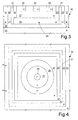
- lateral current flow it is possible to save on the production of some dedicated layers or regions, but the area required for integration is wider, as may be noted from the comparison between Figures 1 to 4 regarding PNP transistors.
- Figures 1 and 2 illustrate a vertical-current-flow PNP transistor formed in a body 1 and comprising an epitaxial layer 2 of N - type accommodating a first buried layer 3, of P + type; a second buried layer 4, of N + type, on top of the first buried layer 3; an insulation region 5, of N + type and annular shape, extending from the surface of the body 1 as far as the second buried layer 4 and surrounding an insulated region 6; a collector well 7, of P type, inside the insulated region 6; a collector contact region 8, of P + type and an annular shape, extending inside the collector well 6; a base well 10, of N type, extending inside the collector well 6 and surrounded by the collector-contact region 8; and an emitter region 11, of P + type, inside the base well 10.
- Figures 3 and 4 illustrate a lateral-current-flow PNP transistor formed in a body 20, comprising an epitaxial layer 21, of N - type, accommodating a first buried layer 22, of P + type; an insulation region 23, of P + type and annular shape, extending from the surface of the body 20 as far as the first buried layer 22 and surrounding an insulated region 26; a second buried layer 24, of N + type, on top of the first buried layer 22 inside the insulated region 26; a deep base region 25, of N + type and annular shape, extending inside the insulated region 26 as far as the second buried layer 24; a base well 27, of N type, surrounded by the deep base region 25 and, underneath, by the second buried layer 24; a collector region 28, of P + type and annular shape, inside the base well 27; and an emitter region 29, of P + type, surrounded by the collector region 28.
- the electrical performance of the lateral-current-flow transistor is regulated mainly by the geometry of the collector region 28 and of the emitter region 29, which are annular and concentric.
- the current gain h FE depends upon the distance between the collector region 28 and the emitter region 29 and upon the charge of the base well 27, whereas the current that can be carried depends upon the facing area between the collector region 28 and the emitter region 29, which is proportional to the perimeter or circumference thereof.
- the aim of the present invention is to provide a lateral-current-flow bipolar transistor able to carry a greater amount of current than known solutions, without increasing significantly the surface area.
- a lateral-current-flow bipolar transistor as defined in claim 1.
- the transistor comprises a base well with a first conductivity type, which accommodates conductive regions with a second conductivity type forming emitter and collector regions.
- One of the emitter and collector regions comprises an internal conductive region and an external conductive region, wherein the external conductive region has an annular shape and the internal conductive region extends internally and at a distance from the external conductive region, and another of the emitter and collector regions comprises an intermediate conductive region, of an annular shape, which extends between and at a distance from the internal and external conductive regions.
- Figures 5 and 6 illustrate an embodiment of a lateral-current-flow PNP transistor formed in a body 50 comprising a substrate 51, of N + type, and an epitaxial layer 52, of N - type, formed by a bottom portion 52a and by a top portion 52b.
- a first buried layer 53, of P + type extends between the bottom portion 52a and the top portion 52b of the epitaxial layer 52;
- an insulation region 54, of P + type and annular shape extends from the surface of the body 50 as far as the first buried layer 53, and delimits, together with the latter, an insulated region 56.
- a second buried layer 55, of N + type, extends inside the insulated region 56 on top of and in contact with the first buried layer 53; a deep base region 57, of N + type and annular shape, extends inside the insulated region 56 as far as the second buried layer 55, and delimits, in the top portion 52b of the epitaxial layer 52, a base well 58.
- the base well 58 accommodates an external collector region 60, of P + type and annular shape; an emitter region 61, of P + type and annular shape, surrounded by the external collector region 60; and an internal collector region 62, of P + type and circular shape, surrounded by the emitter region 61.
- An insulating layer 70 extends on top of the body 50 and accommodates metal contacts and connection lines, enabling electrical connection of the various regions; in particular, the collector regions 60, 62 are electrically connected to a same collector electrode C by a collector-connection region 64 comprising a portion 64b overlying the internal collector region 62; a portion 64c overlying the external collector region 60; and a connection portion 64a extending on top of the emitter region 61.
- the emitter region 61 is connected to an emitter electrode E through a C-shaped emitter-connection region 65 (represented hatched in Figure 6) to enable, in the open area, the passage of the connection portion 64a and the connection between the collector regions 60, 62.
- the collector-connection region 64 and the emitter-connection region 65 are formed in a same metal layer.
- the emitter-collector facing area is considerably increased, without this leading, on the other hand, to any significant increase in the total area.
- a bottom portion 52a of the epitaxial layer 52 is grown.
- concentration and thickness of the bottom portion 52a are chosen appropriately according to the voltage levels required for operation of the finished device.
- the first and second buried layers 53, 55 are then formed on the bottom portion 52a of the epitaxial layer, by ion implantation and a subsequent diffusion, the second buried layer 55 being made with a smaller area and set on top of the first buried layer 53.
- a top portion 52b of the epitaxial layer 52 is grown; then, the insulation region 54 is formed in the top portion 52b of the epitaxial layer 52, by ion implantation and subsequent diffusion step, the insulation region 54 reaching the first buried layer 53 and delimiting, together with the latter, the insulated region 56.
- the deep base region 57 is formed once again by ion implantation and subsequent diffusion step; the deep base region 57 reaches the second buried layer 55 on its edge and delimits, in the top portion 52b of the epitaxial layer 52, the base well 58.
- the collector regions 60, 62 and the emitter region 61, of P + type are formed by ion implantation, in a concentric way with respect to one another.
- the electrical contacts, the electrical-connection regions, and the electrodes E, B, C associated to the different regions of the transistor, are formed on the front surface of the wafer 50, using photolithography and deposition techniques.
- annular-shaped emitter region 61 enables division of the collector region into internal and external portions (collector regions 62, 60), which are electrically connected in parallel by a metal connection region, and hence enables maximization of the facing area between emitter and collector, which now comprises both the external and the internal lateral surfaces of the emitter region. Consequently, the emitter current is higher than in a known PNP transistor thanks to the ratio between the total length of the respective circumferences (a total length which, for the emitter region 61, comprises both the internal and the external circumferences, as indicated in the figure).
- the area of silicon occupied by the transistor according to the invention is much smaller in known PNP transistors.
- the described structure enables two PNP transistors to be obtained which have the same emitter and independent collectors, the currents whereof are in proportion to the internal circumference/external circumference of the emitter region. In this way, the so-called "matched transistors" solution is obtained, without, on the other hand, any need to design two transistors close to one another, which calls for more space.
- the structure described herein enables, as indicated, provision of two transistors with different values of h FE .
- each of the collector regions at an appropriate distance from the emitter region, thereby effectively adjusting the facing area between the emitter and each collector region, it is possible to obtain any combination of h FE gains, with a considerable advantage in space as compared to a traditional solution that uses two distinct transistors having different gains.
- the same solution may be used for NPN transistors by reversing the conductivity type of the various regions, should the process envisage corresponding layers and steps, or by adding a single layer.
- the exact shape of the different regions may vary.
- an additional emitter ring and an additional collector ring may be provided outside the regions 60-62.
Landscapes
- Bipolar Transistors (AREA)
- Bipolar Integrated Circuits (AREA)
Applications Claiming Priority (2)
| Application Number | Priority Date | Filing Date | Title |
|---|---|---|---|
| ITTO20021090 | 2002-12-17 | ||
| IT001090A ITTO20021090A1 (it) | 2002-12-17 | 2002-12-17 | Transistore bipolare a flusso di corrente laterale con alto rapporto perimetro/area di emettitore. |
Publications (2)
| Publication Number | Publication Date |
|---|---|
| EP1432041A2 true EP1432041A2 (fr) | 2004-06-23 |
| EP1432041A3 EP1432041A3 (fr) | 2005-04-27 |
Family
ID=32375574
Family Applications (1)
| Application Number | Title | Priority Date | Filing Date |
|---|---|---|---|
| EP03104650A Withdrawn EP1432041A3 (fr) | 2002-12-17 | 2003-12-11 | Transitor bipolaire à courant latéral et émetteur ayant un rapport perimètre/surface élevé |
Country Status (3)
| Country | Link |
|---|---|
| US (1) | US20040178474A1 (fr) |
| EP (1) | EP1432041A3 (fr) |
| IT (1) | ITTO20021090A1 (fr) |
Cited By (1)
| Publication number | Priority date | Publication date | Assignee | Title |
|---|---|---|---|---|
| WO2009057003A1 (fr) * | 2007-11-01 | 2009-05-07 | Nxp B.V. | Transistor bipolaire à niveau de bruit thermique et de bruit de grenaille réduits |
Families Citing this family (1)
| Publication number | Priority date | Publication date | Assignee | Title |
|---|---|---|---|---|
| FR2987938A1 (fr) * | 2012-03-12 | 2013-09-13 | St Microelectronics Sa | Dispositif electronique de protection contre les decharges electrostatiques, a structure concentrique |
Family Cites Families (6)
| Publication number | Priority date | Publication date | Assignee | Title |
|---|---|---|---|---|
| US4794277A (en) * | 1986-01-13 | 1988-12-27 | Unitrode Corporation | Integrated circuit under-voltage lockout |
| DE3638923A1 (de) * | 1986-11-14 | 1988-05-26 | Telefunken Electronic Gmbh | Integrierte schaltungsanordnung |
| DE69326340T2 (de) * | 1993-09-27 | 2000-01-13 | Stmicroelectronics S.R.L., Agrate Brianza | Geräuscharmer pnp-Transistor |
| JPH0964053A (ja) * | 1995-08-18 | 1997-03-07 | Mitsubishi Electric Corp | ラテラル型トランジスタ |
| FR2762139B1 (fr) * | 1997-04-15 | 1999-07-02 | Sgs Thomson Microelectronics | Transistor pnp lateral dans une technologie bicmos |
| JP2002203956A (ja) * | 2000-12-28 | 2002-07-19 | Mitsubishi Electric Corp | 半導体装置 |
-
2002
- 2002-12-17 IT IT001090A patent/ITTO20021090A1/it unknown
-
2003
- 2003-12-11 EP EP03104650A patent/EP1432041A3/fr not_active Withdrawn
- 2003-12-12 US US10/735,286 patent/US20040178474A1/en not_active Abandoned
Cited By (1)
| Publication number | Priority date | Publication date | Assignee | Title |
|---|---|---|---|---|
| WO2009057003A1 (fr) * | 2007-11-01 | 2009-05-07 | Nxp B.V. | Transistor bipolaire à niveau de bruit thermique et de bruit de grenaille réduits |
Also Published As
| Publication number | Publication date |
|---|---|
| EP1432041A3 (fr) | 2005-04-27 |
| ITTO20021090A1 (it) | 2004-06-18 |
| US20040178474A1 (en) | 2004-09-16 |
Similar Documents
| Publication | Publication Date | Title |
|---|---|---|
| US8492867B2 (en) | Semiconductor device including cell region and peripheral region having high breakdown voltage structure | |
| US6818947B2 (en) | Buried gate-field termination structure | |
| JPH077094A (ja) | BiCDMOS構造及びその製造方法 | |
| JPH0336311B2 (fr) | ||
| US20040048428A1 (en) | Semiconductor device and method of manufacturing the same | |
| US4652895A (en) | Zener structures with connections to buried layer | |
| JP2005322700A (ja) | 半導体装置及びその製造方法 | |
| KR20010106231A (ko) | 반도체장치 | |
| JPH0646638B2 (ja) | 縦型バイポーラ・トランジスタ及びその製造方法 | |
| JP4416288B2 (ja) | 逆導通サイリスタ | |
| US20050127470A1 (en) | Dielectric isolation type semiconductor device and method for manufacturing the same | |
| CN119342872B (zh) | 半导体器件、功率模块、转换电路、车辆及器件制备方法 | |
| US20040178474A1 (en) | Lateral-current-flow bipolar transistor with high emitter perimeter/area ratio | |
| CN217691182U (zh) | 电子装置 | |
| JP3180672B2 (ja) | 半導体装置 | |
| JPWO2003092078A1 (ja) | 半導体素子及びその製造方法 | |
| US6137147A (en) | Bipolar transistor and semiconductor integrated circuit device | |
| JPH10135489A (ja) | ダイオード | |
| KR100216733B1 (ko) | 집적주입논리형 바이폴라 트랜지스터 | |
| JP3149513B2 (ja) | 半導体装置 | |
| JP4287419B2 (ja) | 半導体装置 | |
| JP2004335758A (ja) | ダイオード素子及びその製法 | |
| JP3152290B2 (ja) | 容量素子を含む半導体装置の製造方法 | |
| JP2521745Y2 (ja) | フォトサイリスタ | |
| KR0163924B1 (ko) | 수평형 트랜지스터 및 그 제조방법 |
Legal Events
| Date | Code | Title | Description |
|---|---|---|---|
| PUAI | Public reference made under article 153(3) epc to a published international application that has entered the european phase |
Free format text: ORIGINAL CODE: 0009012 |
|
| AK | Designated contracting states |
Kind code of ref document: A2 Designated state(s): AT BE BG CH CY CZ DE DK EE ES FI FR GB GR HU IE IT LI LU MC NL PT RO SE SI SK TR |
|
| AX | Request for extension of the european patent |
Extension state: AL LT LV MK |
|
| PUAL | Search report despatched |
Free format text: ORIGINAL CODE: 0009013 |
|
| AK | Designated contracting states |
Kind code of ref document: A3 Designated state(s): AT BE BG CH CY CZ DE DK EE ES FI FR GB GR HU IE IT LI LU MC NL PT RO SE SI SK TR |
|
| AX | Request for extension of the european patent |
Extension state: AL LT LV MK |
|
| AKX | Designation fees paid | ||
| REG | Reference to a national code |
Ref country code: DE Ref legal event code: 8566 |
|
| STAA | Information on the status of an ep patent application or granted ep patent |
Free format text: STATUS: THE APPLICATION IS DEEMED TO BE WITHDRAWN |
|
| 18D | Application deemed to be withdrawn |
Effective date: 20051028 |