EP1432064A1 - HF Modul und Methode zur Anordnung von Durchgangslöchern in einem HF Modul - Google Patents
HF Modul und Methode zur Anordnung von Durchgangslöchern in einem HF Modul Download PDFInfo
- Publication number
- EP1432064A1 EP1432064A1 EP03028710A EP03028710A EP1432064A1 EP 1432064 A1 EP1432064 A1 EP 1432064A1 EP 03028710 A EP03028710 A EP 03028710A EP 03028710 A EP03028710 A EP 03028710A EP 1432064 A1 EP1432064 A1 EP 1432064A1
- Authority
- EP
- European Patent Office
- Prior art keywords
- holes
- hole
- attenuance
- radius
- electromagnetic wave
- Prior art date
- Legal status (The legal status is an assumption and is not a legal conclusion. Google has not performed a legal analysis and makes no representation as to the accuracy of the status listed.)
- Withdrawn
Links
- 238000000034 method Methods 0.000 title claims description 19
- 230000014509 gene expression Effects 0.000 claims description 21
- 230000005540 biological transmission Effects 0.000 claims description 14
- 230000005672 electromagnetic field Effects 0.000 claims description 4
- 239000000758 substrate Substances 0.000 abstract description 15
- 230000000644 propagated effect Effects 0.000 abstract description 4
- 238000005259 measurement Methods 0.000 description 35
- 238000010586 diagram Methods 0.000 description 16
- 230000005855 radiation Effects 0.000 description 9
- 239000004020 conductor Substances 0.000 description 7
- 230000008878 coupling Effects 0.000 description 5
- 238000010168 coupling process Methods 0.000 description 5
- 238000005859 coupling reaction Methods 0.000 description 5
- 230000003247 decreasing effect Effects 0.000 description 3
- 230000007423 decrease Effects 0.000 description 2
- 230000000694 effects Effects 0.000 description 2
- 239000000463 material Substances 0.000 description 2
- 239000002184 metal Substances 0.000 description 2
- 230000001902 propagating effect Effects 0.000 description 2
- 229920006395 saturated elastomer Polymers 0.000 description 2
- 239000003989 dielectric material Substances 0.000 description 1
- 230000001788 irregular Effects 0.000 description 1
- 238000004519 manufacturing process Methods 0.000 description 1
- 238000012986 modification Methods 0.000 description 1
- 230000004048 modification Effects 0.000 description 1
Images







Classifications
-
- H—ELECTRICITY
- H01—ELECTRIC ELEMENTS
- H01P—WAVEGUIDES; RESONATORS, LINES, OR OTHER DEVICES OF THE WAVEGUIDE TYPE
- H01P3/00—Waveguides; Transmission lines of the waveguide type
- H01P3/12—Hollow waveguides
- H01P3/121—Hollow waveguides integrated in a substrate
-
- H—ELECTRICITY
- H01—ELECTRIC ELEMENTS
- H01P—WAVEGUIDES; RESONATORS, LINES, OR OTHER DEVICES OF THE WAVEGUIDE TYPE
- H01P3/00—Waveguides; Transmission lines of the waveguide type
- H01P3/12—Hollow waveguides
- H01P3/127—Hollow waveguides with a circular, elliptic, or parabolic cross-section
Definitions
- the present invention relates to an RF module used for propagating a signal in a high frequency band of microwaves, millimeter waves, or the like and a method for arranging through holes in an RF module.
- a strip line, a waveguide, a dielectric waveguide, and the like are known. They are also known as components of a resonator and a filter for high frequency.
- An example of a module formed by using any of the components for high frequency is an MMIC (Monolithic Microwave Integrated Circuit).
- a dielectric waveguide line is formed by a layer stacking technique in a circuit board of a multilayer structure.
- the structure has a plurality of ground conductors stacked while sandwiching dielectrics and through holes having metalized inner face and provided to make the ground conductors conductive, and electromagnetic waves propagate in a region surrounded by the ground conductors and the through holes.
- the intervals of providing through holes are generally determined in consideration of signal wavelength and dielectric constant of a dielectric substrate.
- Japanese Unexamined Patent Application No. Hei 6-53711 discloses a technique of a waveguide in which through holes are provided at intervals each of which is smaller than a cut-off wavelength.
- Japanese Unexamined Patent Application No. Hei 11-284409 discloses a technique of a waveguide in which through holes are provided at intervals each of which is smaller than the half of a guide wavelength in a travel direction of electromagnetic waves.
- the intervals of providing through holes are determined in consideration of, mainly, a signal wavelength.
- a signal wavelength mainly, a signal wavelength
- the relation between the intervals of providing through holes and a conductor loss, a radiation loss, and the like has not been accurately clarified from mathematic viewpoint.
- the arrangement of through holes considering only the signal wavelength is not always in a true optimum state.
- the present invention has been achieved in consideration of such a problem and its object is to provide an RF module in which arrangement of through holes is optimized so that electromagnetic waves can propagate efficiently and a method of arranging through holes in the RF module.
- an RF module having a plurality of through holes, in which an electromagnetic wave propagates by using a region surrounded by the through holes, wherein the plurality of through holes are arranged so as to satisfy the following conditional expression (A) where d denotes an interval between centers of neighboring through holes and r indicates a radius of each of the through holes. 2.0r ⁇ d ⁇ 10.0r
- arrangement of through holes is specified by the relation between the interval d between centers of neighboring through holes and the radius r of each through hole.
- arrangement of through holes can be optimized irrespective of a signal wavelength and the like.
- the plurality of through holes be arranged so as to satisfy the following conditional expression (A-1). 3.6r ⁇ d ⁇ 4.0r
- the RF module is constructed as a transmission line of which side wall is formed by the plurality of through holes
- the plurality of through holes be arranged so as to satisfy the following conditional expression (A-2). 3.6r ⁇ d ⁇ 10.0r
- the plurality of through holes may be arranged so that attenuation of an electromagnetic wave in a non-propagation region between neighboring through holes is 20 dB or higher.
- the plurality of through holes may be arranged so that attenuation of an electromagnetic wave in a non-propagation region between neighboring through holes is 15 dB or higher.
- the RF module according to the invention and the method of arranging through holes in the RF module according to a first aspect of the invention the RF module having a non-uniform electromagnetic wave intensity distribution, it is preferable that the plurality of through holes be arranged so that the higher the electromagnetic field intensity is in a region, the smaller a center interval d is with respect to the radius r of each through hole.
- the relation between the center interval d and the radius r of each through hole is obtained from the required attenuance of an electromagnetic wave.
- arrangement of the through holes is determined.
- arrangement of through holes is optimized.
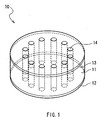
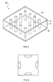
- Figs. 1 and 2 are diagrams for explaining the configuration of an RF module according to an embodiment of the invention and show simplified main components of the RF module.
- the RF modules have a layer-stacked-type waveguide structure using through holes.
- an electromagnetic wave propagation region has a cylindrical shape as a whole.
- an electromagnetic wave propagation region has a rectangular parallelepiped shape as a whole.
- An RF module using any of the layer-stacked-type waveguide is combined with another transmission line, a resonator, and the like and is used as, for example, a transmission line, a filter, or the like for a high frequency signal.
- a cylindrical waveguide 10 has a dielectric substrate 11, ground electrodes 12 and 13 which face each other while sandwiching the dielectric substrate 11, and a plurality of through holes 14 for bringing the ground electrodes 12 and 13 into conduction.
- the inner face of the through hole 14 is metalized.
- the sectional shape of the through hole 14 is an almost circular shape.
- a pseudo conductor wall for electromagnetic waves is formed by the plurality of through holes 14.
- the plurality of through holes 14 are arranged in an almost circular shape as a whole, so that the electromagnetic wave propagation region formed by the through holes 14 and the ground electrodes 12 and 13 has an almost circular shape as a whole.
- the cylindrical waveguide 10 may have a configuration of a dielectric waveguide in which the electromagnetic wave propagation region is filled with a dielectric or a configuration of a cavity waveguide.
- a coupling window for connecting/coupling is provided in a part of the ground electrodes 12 and 13 or a part of a side wall formed by the through holes 14, and another transmission line or the like is connected/coupled via the coupling window indirectly or directly.
- the connecting/coupling structure is not particularly limited to the above but a conventional common technique can be used.
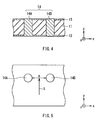
- Figs. 4 and 5 are a partial cross section and a partial plan view of the cylindrical waveguide 10. It can be said that, when seen partially, the cylindrical waveguide 10 has a simple waveguide structure which is covered with electrodes from four sides (up, down, left, and right) by neighboring two through holes 14A and 14B and the ground electrodes 12 and 13.
- the thickness (height) direction of the waveguide is expressed as "z"
- the width direction is expressed as "x”
- a direction orthogonal to the directions "z” and "x” is indicated as “y”.
- center positions in the through holes 14A and 14B will be described as C1 and C2, respectively, the interval of centers of the through holes 14A and 14B will be expressed as “d”, the radius of each of the through holes 14A and 14B will be expressed as "r”, and the shortest distance (through hole gap) between the peripheries of the through holes 14A and 14B will be indicated as "g".
- the through hole gap "g" When it is assumed that the through hole gap "g" is equal to or less than the cut-off wavelength in such a waveguide structure, an electromagnetic wave S propagating in the y direction of Fig. 5 in the through hole gap "g", generally, attenuates exponentially.
- the through holes 14 are arranged so as to satisfy the following conditional expression (A) so that the electromagnetic wave S is not leaked excessively from the gap between the neighboring two through holes 14A and 14B.
- the frequency band of electromagnetic waves is, for example, about 20 GHz to 120 GHz, more preferably, about 20 GHz to 60 GHz. 2.0r ⁇ d ⁇ 10.0r
- the through holes 14 are arranged so as to satisfy the following conditional expression (A-1). 3.6r ⁇ d ⁇ 4.0r
- the through holes 14 are arranged so as to satisfy the following conditional expression (A-2). 3.6r ⁇ d ⁇ 10.0r
- the through holes 14 may be arranged so as to satisfy the following conditional expression together with any of the above conditional expressions.
- ⁇ 0 denotes a wavelength corresponding to a cut-off frequency f0 of frequencies of at least a part of a frequency band used.
- the cylindrical waveguide 10 as a resonator, generally, it is preferable to arrange the plurality of through holes 14 so that attenuation of electromagnetic waves in a non-propagation region between neighboring through holes becomes 20 dB or higher. More preferably, the plurality of through holes 14 are arranged so that the attenuation lies in a range from 25 dB to 30 dB.
- the permissible attenuance may be generally lower than that of a resonator.
- the through holes 14 are arranged so that attenuation of electromagnetic waves is 5 dB or higher, more preferably, 15 dB or higher.
- a rectangular-parallelepiped-shaped waveguide 20 shown in Fig. 2 has a structure substantially similar to that of the cylindrical waveguide 10 shown in Fig. 1 except that the electromagnetic wave propagation region has a rectangular parallelepiped shape.
- the rectangular-parallelepiped-shaped waveguide 20 similarly has a dielectric substrate 21, ground electrodes 22 and 23 which face each other while sandwiching the dielectric substrate 21, and a plurality of through holes 24 for bringing the ground electrodes 22 and 23 into conduction.
- the plurality of through holes 24 are arranged in an almost square shape as a whole. Accordingly, an electromagnetic wave propagation region surrounded by the through holes 24 and the ground electrodes 22 and 23 has an almost rectangular-parallelepiped shape as a whole.
- the through holes 24 have to be provided at intervals each of which is equal to or less than a certain value so that electromagnetic waves do not leak to the outside of the propagation region. In this case, basically, it is sufficient to provide the through holes 24 at intervals similar to those of the cylindrical waveguide 10. In the rectangular-parallelepiped-shaped waveguide 20, however, since the intensity distribution of electromagnetic waves in a wall face portion formed by the through holes 24 is non-uniform, it is desirable to dispose the through holes 24 in consideration of the intensity distribution of the electromagnetic waves.
- Fig. 3 shows an example of the intensity distribution of a magnetic field in an H plane (plane parallel to the magnetic field) in a mode of the lowest order in the rectangular-parallelepiped-shaped waveguide 20.
- the magnetic intensity is high.
- the magnetic field intensity is relatively strong in a center portion of a wall face. It is considered that electromagnetic waves leak more in the region where the electromagnetic wave intensity is strong in the side wall portion formed by the through holes 24.
- the higher the electromagnetic field intensity is the narrower the intervals of providing the through holes 24 are set.
- the center interval "d" to be a value smaller with respect to the radius "r" of a through hole.
- arrangement of the through holes 14 and 24 is specified on the basis of the relation between the interval "d" of centers of neighboring through holes and the radius "r" of each through hole. In such a manner, the arrangement of the through holes 14 and 24 is optimized irrespective of a signal wavelength and the like.
- the attenuance was measured when the interval "d" of centers of neighboring through holes (refer to Fig. 6) was continuously varied while the dielectric constant ⁇ r of the dielectric substrate 11 was fixed to 7.3, the signal frequency f was fixed at 25 GHz, and the through hole radius "r" was fixed to 0.1 mm.
- Fig. 8 is a graph showing the measurement result, in which the horizontal axis indicates frequency (GHz) and the vertical axis denotes the attenuance A (dB). It is understood from the results of the measurement that the value of the attenuance A hardly changes up to around 120 GHz. In particular, up to around 60 GHz, the attenuance A is almost flat. That is, it is understood that the attenuance A hardly depends on the frequency from 20 GHz up to around 120 GHz. A normal frequency used in the waveguide is in a range from 20 GHz to 30 GHz. When the frequency lies in the frequency range, the frequency dependency is at an ignorable level.
- Fig. 9 is a graph showing the measurement result, in which the horizontal axis denotes the dielectric constant ⁇ r and the vertical axis indicates the attenuance A (dB). It is understood from Fig. 9 that the attenuance of the waveguide using the through holes 14 hardly depends on the material of the dielectric substrate 11 within the range of the dielectric which is usually used.
- the attenuance hardly depends on the frequency and the dielectric constant. It is different from the conventional idea, and the results are very interesting. It is estimated that, in the waveguide structure using the through holes 14, the cut-off wavelength is much shorter than the wavelength of an actual signal frequency, so that the attenuance hardly depends on the frequency and the dielectric constant of the substrate but depends on only the cut-off wavelength of the waveguide using the through holes 14.
- Fig. 10 is a graph showing the measurement results, in which the horizontal axis denotes the through hole center interval "d" (mm) and the vertical axis denotes the attenuance A (dB).
- Fig. 11 is a graph obtained by normalizing the through hole interval "d" with the through hole radius "r” and plotting again the measurement results shown in Fig. 10 by using the horizontal axis as d/r. Measurement results are also obtained from the graph that when the ratio between the through hole radius "r” and the through hole center interval "d" is constant, the attenuance is almost the same. The meaning of the phenomenon will now be considered from the physical viewpoint.
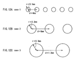
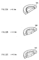
- the arrangements of Figs. 12A, 12B, and 12C will be described below as case 1, case 2, and case 3, respectively.
- the electromagnetic waves passing through the waveguides attenuate at the same attenuance in the cases 1, 2, and 3.
- the case 3 (Fig. 12C) and the case 1 (Fig. 12A) are compared with each other, the interval between through holes in the case 3 is wider, so that an attenuation constant is low.
- the diameter of the through hole 14 in the case 3 is larger, so that the attenuation distance is three times as long as that in the case 1. That is, in the case 3, as compared with the case 1, the interval between the through holes is wide, so that the attenuance per unit length is low.
- the attenuation distance is long, so that the low attenuance is canceled off and the attenuance as a whole becomes the same as that in the case 1.
- the attenuance of the electromagnetic waves by the through holes can be understood to a certain degree. There must be some correlation between the attenuance A and the no load Q of the resonator.
- the no load Q in a dominant mode in the case where the cylindrical waveguide 10 is used as a resonator was measured and the result of measurement was verified.
- Figs. 13A to 13G show arrangement patterns of the through holes 14 in the cylindrical waveguide resonator to be measured.
- the through holes 14 are arranged so as to have rotation symmetry of an angle ⁇ .
- the angles ⁇ in the arrangement patterns in Figs. 13A to 13G are 30°, 24°, 20°, 18°, 15°, 12°, and 10°, respectively.
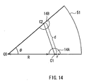
- the angle ⁇ denotes an angle formed by, as shown in Fig. 14, two straight lines connecting the center position C0 of the whole resonator and the center positions C1 and C2 of neighboring through holes 14A and 14B.
- the cylindrical waveguide resonators of Figs. 13A to 13G are designed so as to resonate when the radius "r" of each through hole is 0.1 mm, the dielectric constant ⁇ r of a dielectric (s39 material) is 7.3, and the frequency is about 25 GHz.
- the length from the center position C0 of the whole resonator to the outermost face 51 of the resonator (refer to Fig. 14) is 3.0 mm and the length R from the resonator center C0 to the through hole 14 is 1.7 mm.
- the cylindrical resonator is used as a measurement model, the following points can be mentioned; a point that the dominant mode of the cylindrical resonator does not have dependency on the angle direction and the condition is the same with respect to all of the through holes 14 (in the case of the rectangular-parallelepiped-shaped resonator, the magnetic field intensity distributes in an sin function on the waveguide wall face) and a point that the electromagnetic wave is perpendicularly incident on the waveguide wall face constructed by the through holes 14.
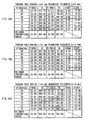
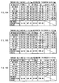
- Figs. 15A to 15C show the measurement results. Measurement was conducted with respect to three kinds of the thickness "h" of the resonator of 0.2 mm, 0.3 mm, and 0.4 mm.
- "f” and “Q” are values of the resonance frequency and the no load Q, respectively, in the case where the outermost surface 51 of the resonator is covered with a metal (in the case where ⁇ is 3.0E7, that is, zero radiation loss).
- "fr” and “Qr” denote values in the case where the electric conductivity ⁇ of the outermost surface 51 is set to 1 (that is, with a radiation loss).
- Fig. 16 shows the relation between the rotation symmetry angle ⁇ and r/d in the cylindrical waveguide resonators of Figs. 13A to 13G.
- the value of the radius "r" of a through hole in this case is 0.1 mm as described above.
- the rotation symmetrical angle ⁇ has to be increased.
- the no load Q is saturated at a value around the theoretical value when the attenuance A is about 26 dB in the non-propagation region between the through holes 14A and 14B.
- the center interval "d" is wide (the angle ⁇ is large) and sufficient attenuation is not obtained, electromagnetic waves are leaked and a radiation loss occurs. Consequently, as compared with the no load Q (Q) measured with no radiation loss, the no load Q (Qr) deteriorates more conspicuously.
- Fig. 20 is a graph showing the relation between the attenuance A in a through hole part and the no load Q (Qr) obtained from the measurement results, in which the horizontal axis denotes the attenuance A (dB) and the vertical axis indicates the no load Q.
- through holes are arranged at intervals each of which is equal to or less than the cut-off wavelength.
- the interval is not limited to the cut-off wavelength or less.
- the through holes may be arranged so as to satisfy, for example, the following conditional expression together with the above-described conditional expressions.
- ⁇ 0 denotes a wavelength corresponding to a cut-off frequency f0 of at least a part of the frequencies in a frequency band used.
- Figs. 21A to 21C and Figs. 22A to 22C show concrete configuration examples of a preferred cylindrical resonator obtained from the above-described measurement results. In the diagrams, the configurations are simplified and shown partially. The basic general configuration is similar to that of the cylindrical waveguide 10 shown in Fig. 1.
- the cylindrical resonators are structure examples in which attenuation of about 38 dB is obtained in a through hole part, and thickness "h" is 0.4 mm.
- the radiuses "r" of through holes 54A, 54B, and 54C are 0.1 mm, 0.2 mm, and 0.3 mm, respectively.
- the no load Q is about 530 which is almost the same as the no load Q of the theoretical value.
- an equivalent no load Q is obtained in the case where the radius "r" of the through hole is set to be large, by accordingly widening the center interval "d", an equivalent no load Q is obtained. That is, it means that it was proved that by increasing the through hole radius, the number of through holes can be decreased.
- the interval of the through holes 14 provided in the substrate 11 has to be considered on the basis of, not the wavelength, but the ratio between the through hole radius "r" and the through hole center interval "d".
- arrangement of through holes is specified on the basis of the relation between the interval "d" of centers of neighboring through holes and the radius "r" of each through hole.
- arrangement of through holes can be optimized irrespective of a signal wavelength and the like.
- the present invention is not limited to the foregoing embodiments but can be variously modified.
- the example of the configuration that the ground electrode is formed by two layers has been described in the foregoing embodiment, the invention can be also applied to a multilayered structure having a ground electrode of three or more layers.
- the method of arranging through holes according to the invention can be applied not only to the cylindrical waveguide 10 and the rectangular-parallelepiped waveguide 20 but also other waveguides each having a layer-stacked structure using through holes.
- sectional shape of a through hole is a circle
- sectional shape may be a polygonal shape similar to a circle, an oval shape close to a circle, or the like, by using similar arrangement, similar effects may be obtained. It can be also considered that even when the radiuses "r" of through holes are not the same but are at least in a range of a manufacture error or the like, by using similar arrangement, similar effects may be obtained.
- arrangement of through holes is specified on the basis of the relation between the center interval "d" of neighboring through holes and the radius "r" of a through hole. Consequently, arrangement of the through holes can be optimized irrespective of a signal wavelength and the like.
- electromagnetic waves can be propagated efficiently.
- the relation between the center interval "d" of neighboring through holes and the radius "r" of a through hole is obtained from the required attenuance of electromagnetic waves.
- arrangement of through holes is determined.
- arrangement of through holes can be optimized irrespective of a signal wavelength and the like.
Landscapes
- Control Of Motors That Do Not Use Commutators (AREA)
- Waveguides (AREA)
Applications Claiming Priority (2)
| Application Number | Priority Date | Filing Date | Title |
|---|---|---|---|
| JP2002364054 | 2002-12-16 | ||
| JP2002364054A JP4015938B2 (ja) | 2002-12-16 | 2002-12-16 | 共振器 |
Publications (1)
| Publication Number | Publication Date |
|---|---|
| EP1432064A1 true EP1432064A1 (de) | 2004-06-23 |
Family
ID=32376213
Family Applications (1)
| Application Number | Title | Priority Date | Filing Date |
|---|---|---|---|
| EP03028710A Withdrawn EP1432064A1 (de) | 2002-12-16 | 2003-12-12 | HF Modul und Methode zur Anordnung von Durchgangslöchern in einem HF Modul |
Country Status (4)
| Country | Link |
|---|---|
| US (1) | US6992548B2 (de) |
| EP (1) | EP1432064A1 (de) |
| JP (1) | JP4015938B2 (de) |
| CN (1) | CN1277332C (de) |
Families Citing this family (13)
| Publication number | Priority date | Publication date | Assignee | Title |
|---|---|---|---|---|
| JP3845394B2 (ja) * | 2003-06-24 | 2006-11-15 | Tdk株式会社 | 高周波モジュール |
| US7205948B2 (en) * | 2005-05-24 | 2007-04-17 | Raytheon Company | Variable inclination array antenna |
| US7965251B2 (en) * | 2006-09-20 | 2011-06-21 | Alcatel-Lucent Usa Inc. | Resonant cavities and method of manufacturing such cavities |
| US8324989B2 (en) * | 2006-09-20 | 2012-12-04 | Alcatel Lucent | Re-entrant resonant cavities and method of manufacturing such cavities |
| CN100444461C (zh) * | 2006-09-22 | 2008-12-17 | 东南大学 | 基片集成波导准感性通孔滤波器 |
| CN100433449C (zh) * | 2006-10-17 | 2008-11-12 | 东南大学 | 双通带频率选择表面 |
| CN100433448C (zh) * | 2006-10-17 | 2008-11-12 | 东南大学 | 超薄单边陡降滤波特性频率选择表面 |
| WO2009081504A1 (en) * | 2007-12-25 | 2009-07-02 | Nec Corporation | Differential-common mode resonant filters |
| CA2629035A1 (en) * | 2008-03-27 | 2009-09-27 | Her Majesty The Queen In Right Of Canada, As Represented By The Minister Of Industry, Through The Communications Research Centre Canada | Waveguide filter with broad stopband based on sugstrate integrated waveguide scheme |
| CN105226360B (zh) * | 2015-08-24 | 2018-05-29 | 上海交通大学 | 基片集成同轴波导互连阵列结构 |
| JP6680928B1 (ja) | 2019-05-10 | 2020-04-15 | 株式会社フジクラ | モード変換器及びモード変換器の製造方法 |
| JP7129499B2 (ja) * | 2020-01-16 | 2022-09-01 | 株式会社フジクラ | 基板及びアンテナモジュール |
| EP4270633A4 (de) | 2020-12-25 | 2024-11-13 | Kyocera Corporation | Leiterplatte, gestapelter resonator und gestapeltes filter |
Citations (3)
| Publication number | Priority date | Publication date | Assignee | Title |
|---|---|---|---|---|
| JPH0653711A (ja) * | 1992-07-28 | 1994-02-25 | Fukushima Nippon Denki Kk | 導波管線路 |
| JPH11284409A (ja) * | 1998-03-27 | 1999-10-15 | Kyocera Corp | 導波管型帯域通過フィルタ |
| US6356172B1 (en) * | 1999-12-29 | 2002-03-12 | Nokia Networks Oy | Resonator structure embedded in mechanical structure |
Family Cites Families (9)
| Publication number | Priority date | Publication date | Assignee | Title |
|---|---|---|---|---|
| JPS6271305A (ja) * | 1985-09-24 | 1987-04-02 | Murata Mfg Co Ltd | 誘電体共振器 |
| FR2671232B1 (fr) * | 1990-12-27 | 1993-07-30 | Thomson Csf | Charge pour ligne triplaque hyperfrequences a substrat dielectrique. |
| JP3493265B2 (ja) | 1996-09-30 | 2004-02-03 | 京セラ株式会社 | 誘電体導波管線路および配線基板 |
| US6133805A (en) * | 1996-10-31 | 2000-10-17 | The Whitaker Corporation | Isolation in multi-layer structures |
| JP3464104B2 (ja) | 1996-10-31 | 2003-11-05 | 京セラ株式会社 | 積層型導波管線路の結合構造 |
| JP3366552B2 (ja) * | 1997-04-22 | 2003-01-14 | 京セラ株式会社 | 誘電体導波管線路およびそれを具備する多層配線基板 |
| US6057747A (en) * | 1997-08-22 | 2000-05-02 | Kyocera Corporation | Dielectric waveguide line and its branch structure |
| JPH1168416A (ja) | 1997-08-22 | 1999-03-09 | Kyocera Corp | 誘電体導波管線路 |
| DE60208244T2 (de) * | 2001-01-12 | 2006-06-29 | Murata Manufacturing Co., Ltd., Nagaokakyo | Übertragungsleitunganordnung, integrierte Schaltung und Sender-Empfängergerät |
-
2002
- 2002-12-16 JP JP2002364054A patent/JP4015938B2/ja not_active Expired - Fee Related
-
2003
- 2003-12-12 US US10/733,349 patent/US6992548B2/en not_active Expired - Lifetime
- 2003-12-12 EP EP03028710A patent/EP1432064A1/de not_active Withdrawn
- 2003-12-16 CN CNB2003101206535A patent/CN1277332C/zh not_active Expired - Fee Related
Patent Citations (3)
| Publication number | Priority date | Publication date | Assignee | Title |
|---|---|---|---|---|
| JPH0653711A (ja) * | 1992-07-28 | 1994-02-25 | Fukushima Nippon Denki Kk | 導波管線路 |
| JPH11284409A (ja) * | 1998-03-27 | 1999-10-15 | Kyocera Corp | 導波管型帯域通過フィルタ |
| US6356172B1 (en) * | 1999-12-29 | 2002-03-12 | Nokia Networks Oy | Resonator structure embedded in mechanical structure |
Non-Patent Citations (4)
| Title |
|---|
| ITO M ET AL: "A 60 GHZ-BAND PLANAR DIELECTRIC WAVEGUIDE FILTER FOR FLIP-CHIP MODULES", 2001 IEEE MTT-S INTERNATIONAL MICROWAVE SYMPOSIUM DIGEST.(IMS 2001). PHOENIX, AZ, MAY 20 - 25, 2001, IEEE MTT-S INTERNATIONAL MICROWAVE SYMPOSIUM, NEW YORK, NY: IEEE, US, vol. 3 OF 3, 20 May 2001 (2001-05-20), pages 1597 - 1600, XP001067527, ISBN: 0-7803-6538-0 * |
| PATENT ABSTRACTS OF JAPAN vol. 018, no. 280 (E - 1555) 27 May 1994 (1994-05-27) * |
| PATENT ABSTRACTS OF JAPAN vol. 2000, no. 01 31 January 2000 (2000-01-31) * |
| UCHIMURA H ET AL: "DEVELOPMENT OF A LAMINATED WAVEGUIDE", IEEE TRANSACTIONS ON MICROWAVE THEORY AND TECHNIQUES, IEEE INC. NEW YORK, US, vol. 46, no. 12, PART 2, December 1998 (1998-12-01), pages 2438 - 2443, XP000805624, ISSN: 0018-9480 * |
Also Published As
| Publication number | Publication date |
|---|---|
| JP2004200783A (ja) | 2004-07-15 |
| JP4015938B2 (ja) | 2007-11-28 |
| CN1508904A (zh) | 2004-06-30 |
| US6992548B2 (en) | 2006-01-31 |
| US20040145434A1 (en) | 2004-07-29 |
| CN1277332C (zh) | 2006-09-27 |
Similar Documents
| Publication | Publication Date | Title |
|---|---|---|
| US5986527A (en) | Planar dielectric line and integrated circuit using the same line | |
| US7199680B2 (en) | RF module using mode converting structure having short-circuiting waveguides and connecting windows | |
| US6977566B2 (en) | Filter and method of arranging resonators | |
| US7227428B2 (en) | RF module and mode converting structure having magnetic field matching and penetrating conductor patterns | |
| US6992548B2 (en) | RF module and method for arranging through holes in RF module | |
| KR100287258B1 (ko) | 유전체공진기,유전체필터,듀플렉서및통신장치 | |
| US11158919B2 (en) | Band-pass filter comprising a substrate enclosed by conductive layer pairs and a post wall to define a plurality of resonators having recesses of different depths | |
| JP2991076B2 (ja) | 平面誘電体線路及び集積回路 | |
| KR100276012B1 (ko) | 유전체필터와 송수신듀플렉서 및 통신기기 | |
| KR100540933B1 (ko) | 고주파 회로 장치 및 송수신 장치 | |
| CN114788087B (zh) | 多层带通滤波器 | |
| US7403085B2 (en) | RF module | |
| US6525625B1 (en) | Dielectric duplexer and communication apparatus | |
| US6498543B2 (en) | Monoblock dielectric duplexer | |
| KR100297346B1 (ko) | 유전체필터및이를이용한통신장치 | |
| JP3264214B2 (ja) | 非放射性平面誘電体線路およびその集積回路 | |
| US6166614A (en) | Nonradiative planar dielectric line and integrated circuit | |
| JPH09246821A (ja) | 誘電体共振器および帯域通過フィルタ | |
| HK40081933A (en) | A multi-layer bandpass filter | |
| JP2004032471A (ja) | 分波回路および分波装置 |
Legal Events
| Date | Code | Title | Description |
|---|---|---|---|
| PUAI | Public reference made under article 153(3) epc to a published international application that has entered the european phase |
Free format text: ORIGINAL CODE: 0009012 |
|
| AK | Designated contracting states |
Kind code of ref document: A1 Designated state(s): AT BE BG CH CY CZ DE DK EE ES FI FR GB GR HU IE IT LI LU MC NL PT RO SE SI SK TR |
|
| AX | Request for extension of the european patent |
Extension state: AL LT LV MK |
|
| 17P | Request for examination filed |
Effective date: 20041025 |
|
| AKX | Designation fees paid |
Designated state(s): DE FR GB SE |
|
| 17Q | First examination report despatched |
Effective date: 20050217 |
|
| STAA | Information on the status of an ep patent application or granted ep patent |
Free format text: STATUS: THE APPLICATION IS DEEMED TO BE WITHDRAWN |
|
| 18D | Application deemed to be withdrawn |
Effective date: 20060719 |