EP1432843B1 - Verfahren zur herstellung eines films aus kohlenstoffdotiertem oxid - Google Patents
Verfahren zur herstellung eines films aus kohlenstoffdotiertem oxid Download PDFInfo
- Publication number
- EP1432843B1 EP1432843B1 EP02800893A EP02800893A EP1432843B1 EP 1432843 B1 EP1432843 B1 EP 1432843B1 EP 02800893 A EP02800893 A EP 02800893A EP 02800893 A EP02800893 A EP 02800893A EP 1432843 B1 EP1432843 B1 EP 1432843B1
- Authority
- EP
- European Patent Office
- Prior art keywords
- carbon doped
- doped oxide
- oxygen
- substrate
- sccm
- Prior art date
- Legal status (The legal status is an assumption and is not a legal conclusion. Google has not performed a legal analysis and makes no representation as to the accuracy of the status listed.)
- Expired - Lifetime
Links
Images



Classifications
-
- H—ELECTRICITY
- H10—SEMICONDUCTOR DEVICES; ELECTRIC SOLID-STATE DEVICES NOT OTHERWISE PROVIDED FOR
- H10P—GENERIC PROCESSES OR APPARATUS FOR THE MANUFACTURE OR TREATMENT OF DEVICES COVERED BY CLASS H10
- H10P14/00—Formation of materials, e.g. in the shape of layers or pillars
- H10P14/60—Formation of materials, e.g. in the shape of layers or pillars of insulating materials
- H10P14/69—Inorganic materials
- H10P14/692—Inorganic materials composed of oxides, glassy oxides or oxide-based glasses
- H10P14/6921—Inorganic materials composed of oxides, glassy oxides or oxide-based glasses containing silicon
- H10P14/6922—Inorganic materials composed of oxides, glassy oxides or oxide-based glasses containing silicon the material containing Si, O and at least one of H, N, C, F or other non-metal elements, e.g. SiOC, SiOC:H or SiONC
-
- C—CHEMISTRY; METALLURGY
- C23—COATING METALLIC MATERIAL; COATING MATERIAL WITH METALLIC MATERIAL; CHEMICAL SURFACE TREATMENT; DIFFUSION TREATMENT OF METALLIC MATERIAL; COATING BY VACUUM EVAPORATION, BY SPUTTERING, BY ION IMPLANTATION OR BY CHEMICAL VAPOUR DEPOSITION, IN GENERAL; INHIBITING CORROSION OF METALLIC MATERIAL OR INCRUSTATION IN GENERAL
- C23C—COATING METALLIC MATERIAL; COATING MATERIAL WITH METALLIC MATERIAL; SURFACE TREATMENT OF METALLIC MATERIAL BY DIFFUSION INTO THE SURFACE, BY CHEMICAL CONVERSION OR SUBSTITUTION; COATING BY VACUUM EVAPORATION, BY SPUTTERING, BY ION IMPLANTATION OR BY CHEMICAL VAPOUR DEPOSITION, IN GENERAL
- C23C16/00—Chemical coating by decomposition of gaseous compounds, without leaving reaction products of surface material in the coating, i.e. chemical vapour deposition [CVD] processes
- C23C16/22—Chemical coating by decomposition of gaseous compounds, without leaving reaction products of surface material in the coating, i.e. chemical vapour deposition [CVD] processes characterised by the deposition of inorganic material, other than metallic material
- C23C16/30—Deposition of compounds, mixtures or solid solutions, e.g. borides, carbides, nitrides
- C23C16/40—Oxides
- C23C16/401—Oxides containing silicon
-
- H—ELECTRICITY
- H10—SEMICONDUCTOR DEVICES; ELECTRIC SOLID-STATE DEVICES NOT OTHERWISE PROVIDED FOR
- H10P—GENERIC PROCESSES OR APPARATUS FOR THE MANUFACTURE OR TREATMENT OF DEVICES COVERED BY CLASS H10
- H10P14/00—Formation of materials, e.g. in the shape of layers or pillars
- H10P14/60—Formation of materials, e.g. in the shape of layers or pillars of insulating materials
- H10P14/63—Formation of materials, e.g. in the shape of layers or pillars of insulating materials characterised by the formation processes
- H10P14/6326—Deposition processes
- H10P14/6328—Deposition from the gas or vapour phase
- H10P14/6334—Deposition from the gas or vapour phase using decomposition or reaction of gaseous or vapour phase compounds, i.e. chemical vapour deposition
- H10P14/6336—Deposition from the gas or vapour phase using decomposition or reaction of gaseous or vapour phase compounds, i.e. chemical vapour deposition in the presence of a plasma [PECVD]
-
- H—ELECTRICITY
- H10—SEMICONDUCTOR DEVICES; ELECTRIC SOLID-STATE DEVICES NOT OTHERWISE PROVIDED FOR
- H10P—GENERIC PROCESSES OR APPARATUS FOR THE MANUFACTURE OR TREATMENT OF DEVICES COVERED BY CLASS H10
- H10P14/00—Formation of materials, e.g. in the shape of layers or pillars
- H10P14/60—Formation of materials, e.g. in the shape of layers or pillars of insulating materials
- H10P14/66—Formation of materials, e.g. in the shape of layers or pillars of insulating materials characterised by the type of materials
- H10P14/668—Formation of materials, e.g. in the shape of layers or pillars of insulating materials characterised by the type of materials the materials being characterised by the deposition precursor materials
- H10P14/6681—Formation of materials, e.g. in the shape of layers or pillars of insulating materials characterised by the type of materials the materials being characterised by the deposition precursor materials the precursor containing a compound comprising Si
- H10P14/6684—Formation of materials, e.g. in the shape of layers or pillars of insulating materials characterised by the type of materials the materials being characterised by the deposition precursor materials the precursor containing a compound comprising Si the compound comprising silicon and oxygen
- H10P14/6686—Formation of materials, e.g. in the shape of layers or pillars of insulating materials characterised by the type of materials the materials being characterised by the deposition precursor materials the precursor containing a compound comprising Si the compound comprising silicon and oxygen the compound being a molecule comprising at least one silicon-oxygen bond and the compound having hydrogen or an organic group attached to the silicon or oxygen, e.g. a siloxane
Definitions
- the present invention relates to semiconductor layer deposition.
- the present invention relates to carbon doped oxide deposition.
- capacitance (C) can be viewed as k ⁇ A d where (d) is the distance between the conductive lines 275 as shown in Fig. 2c, (A), the area of each conductive line interface, ( ⁇ ), the permeability of the ILD, and (k), the dielectric constant (a factor of how much effect the ILD material has on capacitor value).
- the dielectric constant (k) noted above has no units of measure. For example, where the dielectric is of a vacuum or air, the dielectric constant (k) is about equal to 1, having no effect on capacitance. However, most intra-layer dielectric materials have a degree of polarity with a dielectric constant (k) above 1. For example, silicon dioxide, a common ILD material, has a dielectric constant generally exceeding about 4. Due to the decreasing size of semiconductor features (e.g., reduced distance (d) leading to increased capacitance (C)), efforts have recently been made to reduce the dielectric constant (k) of the ILD as a means by which to reduce capacitance (C). That is, where capacitance (C) is k ⁇ A d and all other factors remaining constant, reduction of the dielectric constant (k) can reduce capacitance (C).
- Low dielectric constant (k) materials i.e. 'low k' materials
- FSG fluorinated silica glass
- SILKTM carbon doped oxides
- CDO's carbon doped oxides
- EP-A-1 077 477 discloses a method for forming an insulation layer over a substrate. The method forms a carbon-doped silicone oxide layer by thermal chemical vapor deposition using an organosilane and is particularly suitable for deposition of low dielectric constant films, i.e. where k is less or equal to 3.0.
- US-B 1-6 258 735 discloses a method for depositing a carbon-doped silicon oxide film having a low dielectric constant (k).
- concentration of oxygen is controlled to produce soft plasma conditions inside the chamber while a precursor gas is diverted through a bypass to stabilize the precursor gas flow prior to routing the precursor into the chamber and using a back-to-back plasma deposition scheme.
- WO 99 38202 A discloses a method for treating a substrate, which method comprises positioning the substrate in a chamber, introducing into the chamber in the gaseous or vapor state a silicon-containing compound, a further compound containing peroxide bonding, and a substance which associates readily the compound containing peroxide bonding, the method further comprising the step of reacting the silicon containing compound with the further compound and the soluble substance to provide an isolating layer on the substance.
- the associating substance may be an oxidizing agent such as oxygen.
- Fig. 1 is a side cross-sectional view of an embodiment of a semiconductor substrate in a reactor.
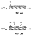
- Fig. 2A is a side cross-sectional view of the substrate of Fig. 1 following deposition of a CDO film.
- Fig. 2B is a side cross-sectional view of the substrate of Fig. 2A following trench etch.
- Fig. 2C is a side cross-sectional view of the substrate of Fig. 2B following formation of conductive metal lines.
- Fig. 3 is a flowchart summarizing an embodiment of semiconductor substrate processing.
- Embodiments described below are generally applicable to processing of a semiconductor substrate. Once a substrate has been obtained, initial processing can include the formation of a dielectric layer above a surface of the substrate. Embodiments described here focus on the deposition of CDO dielectric material, in particular, by introduction of oxygen in the presence of a CDO precursor to increase the rate of CDO deposition.
- a substrate 100 that is exposed to a gas mixture 160 that includes a CDO precursor.
- Oxygen is also included in the gas mixture 160 to increase the rate of CDO deposition on the substrate 100 when, for example, the gas mixture 160 is excited to cause deposition as described further herein.
- the substrate 100 includes an initial dielectric etch-stop layer 120.
- the substrate 100 can be of silicon and other conventional materials.
- the etch-stop layer 120 is not required but is shown for illustration as described further herein. Additionally, in other embodiments of the invention various other insulating or conducting layers and features may be present on the substrate 100 that are not necessarily described here.
- the substrate 100 is placed within a reactor 180 for deposition of a material on the substrate 100.
- the material to be formed on the substrate 100 is a Carbon Doped Oxide (CDO) to act as an ILD.
- CDO material is a material that has incorporated silicon (Si), carbon (C), and oxygen (O), providing relatively reduced polarity, density, and conductivity.
- Si silicon
- C carbon
- O oxygen
- CDO material can have a dielectric constant (k) that is less than about 3.0. Therefore, CDO materials are generally considered 'low k' materials, and useful for lowering capacitance when used as ILD's as discussed further herein.
- the reactor 180 is a conventional chemical vapor deposition (CVD) apparatus.
- the CVD apparatus may be plasma enhanced (i.e. a PECVD apparatus) and operated by conventional means.
- the PECVD apparatus is provided with a shower plate 150 coupled to a power source 155.
- the substrate 100 is grounded and positioned adjacent the shower plate 150.
- the substrate 100 is positioned between about 15mm and about 40mm from the shower plate 150, preferably between about 24mm and about 26mm.
- the gas mixture 160 is introduced into the apparatus in vapor form. Simultaneously, radio frequency (RF) is applied through the PECVD apparatus such that the gas mixture 160 is excited to a plasma state to cause deposition on the surface of the substrate 100.
- RF radio frequency
- at least a portion of the gas mixture 160 is excited to a plasma state at a remote location prior to introduction to the PECVD apparatus. In such an embodiment, this portion of the gas mixture 160 can enter the PECVD apparatus already in a plasma state.
- the gas mixture 160 referenced above includes a CDO precursor and a deposition enhancing gas such as oxygen. As discussed further herein, the inclusion of oxygen increases the rate of deposition and formation of the CDO material.
- An inert gas such as helium (He) can also be provided as part of the gas mixture 160 to serve as a volume-filler within the PECVD apparatus during deposition.
- the inert gas can also be a good heat conductor to promote thermal uniformity. However, it does not actually take part, chemically, in the deposition process.
- other inert gasses such as argon (Ar), neon (Ne), krypton (Kr), and xenon (Xe) can be used as a background gas.
- a CDO precursor which is a part of the gas mixture 160 described above, supplies a source of carbon (C) and silicon (Si) for the formation of CDO features.
- a CDO precursor can also supply a source of oxygen (O). However, this is not required, as oxygen (O) is separately provided according to embodiments described herein.
- Embodiments of CDO precursors include tetramethylcyclotetrasiloxane ((HSiOCH 3 ) 4 ) or (CH 3 ) x Si(OCH 3 ) 4-x .
- dimethyldimethoxysilane (CH 3 ) 2 Si(OCH 3 ) 2 is used as the CDO precursor.
- Such CDO precursors result in a CDO material with a dielectric constant (k) that is less than about 3.0 as described above.
- oxygen gas is supplied to the PECVD apparatus and excited (e.g. O*) by application of RF.
- the oxygen gas supplied as part of the gas mixture 160 can initially be in the form of ionic oxygen (e.g. O 2- ), molecularly stable oxygen (O 2 ), elementally stable oxygen (O), or ozone (O 3 ).
- RF is applied affecting the oxygen gas as it enters the PECVD apparatus such that at least a portion of the oxygen molecules will be in an excited state (e.g. O*).
- the excited oxygen molecules interact with the CDO precursor to increase the rate of CDO deposition.
- oxygen, in the form of ozone (O 3 ) is excited thermally without use of RF to increase the rate of CDO deposition.
- the ozone (O 3 ) form of the oxygen gas is more readily excitable in this manner.
- the oxygen gas is excited, along with the background gas, at a remote location separate from the CDO precursor of the gas mixture 160.
- the CDO precursor is excited upon introduction to the PECVD apparatus, where it combines with the already excited oxygen gas.
- the gas mixture 160 enters the PECVD apparatus, which is energized by introduction of RF.
- the process can proceed within the PECVD apparatus at conventional pressures, temperatures, radio frequency (RF) and power
- pressure is maintained between 266 Pa (2.0 Torr) and 1,333.10 3 Pa (0.0 Torr), preferably between 399 Pa (3.0 Torr) and about 798 Pa (6.0 Torr)
- temperature of the susceptor 135 supporting the substrate 100 is maintained between about 250°C and about 450°C
- RF is maintained at standard frequencies and between about 1,600 watts and about 1,800 watts are supplied.
- the oxygen gas is in an amount that is less than about 5% of the volume taken up by the oxygen- and CDO precursor.
- flow rates, in standard cubic centimeters per minute (sccm) for the individual gasses of the gas mixture 160 can be as follows: Precursor gas flow rate 50-200 sccm Background gas flow rate 20-200 sccm Oxygen gas flow rate 1.0-20 sccm
- CDO deposition rate is between about 562 nm (5,620 angstroms) per minute and about 960 nm (9,600 angstroms) per minute, preferably up to about 958 nm (9,580 angstroms) per minute. This can translate into about a 70% increase in CDO deposition rate as compared to conventional PECVD deposition of CDO without the introduction of oxygen.
- the substrate 100 of the embodiment of Fig. 1 is shown with a CDO film 200 deposited above an etch-stop layer 120.
- the CDO film 200 has a dielectric constant that is less than about 3.0. In one embodiment the CDO film dielectric constant is less than about 2.7. Additionally, deposition of the CDO film 200 in the presence of oxygen may provide a slightly lower dielectric constant, when compared to the deposition of the same CDO film 200 in the absence of oxygen. In the embodiment shown the CDO film 200 is to form a CDO ILD (see Fig. 3). However this is not required.
- the CDO film 200 can be used for a variety of insulating purposes.
- the CDO film 200 is etched to form trenches 250.
- the CDO film 200 is patterned and etched by conventional means.
- a protective mask pattern can be placed above the CDO film 200 exposing areas to form the parallel trenches 250.
- a chemical etchant is then applied to etch through exposed portions of the CDO film 200.
- the etch-stop layer 120 is of a material resistant to chemical etchant and helps control the depth of the etched trenches 250.
- the etch-stop layer 120 can be of silicon nitride (SiN), silicon carbide (SiC), or other conventional etch-stop material.
- the deposited CDO film 200 provides structural support and isolation of conductive lines 275 in the form of a CDO ILD.
- the conductive lines 275 are deposited upon etch of the CDO film 200 to form a CDO ILD down to the etch-stop layer 120.
- the conductive lines 275 are of copper (Cu).
- the etch-stop layer 120 also acts as a barrier to prevent diffusion of copper ions (Cu + ) to below the etch-stop layer 120, therefore maintaining a degree of isolation of the conductive lines 275.
- the conductive lines 275 can be deposited by conventional means.
- an ionized form of conductive line material e.g. Cu +
- RF can be applied to the apparatus to generate a plasma and effect deposition of a conductive layer including the conductive lines 275.
- Other excess of the conductive layer can be removed by conventional Chemical-Mechanical Polishing (CMP) techniques such that the substrate 100 includes a smooth upper surface 290 and further isolating the conductive lines 275 as shown in Fig. 2C.
- CMP Chemical-Mechanical Polishing
- the deposited conductive lines 275 are separated by a distance (d) wherein ILD material 200 is present isolating the conductive lines 275.
- ILD material 200 is present isolating the conductive lines 275.
- capacitance (C) is k ⁇ A d
- reduction in the distance (d) can increase capacitance (C).
- embodiments described here include the use of 'low k' CDO ILD material 200 to compensate for this problem in a manner that does not sacrifice reasonable thruput (e.g. semiconductor processing time) due to lengthy CDO deposition times.
- a substrate is placed in a reactor where a CDO precursor and oxygen are introduced 310.
- Deposition results to form a CDO film on the substrate.
- the deposition takes place in an otherwise conventional manner, such as within a PECVD apparatus operated under conventional conditions. Deposition in this manner takes place at an increased rate due to the presence of oxygen.
- the CDO film is then etched 320.
- Etching 320 of the CDO is achieved by conventional methods, with conventional etchants applied to the CDO film.
- conductive lines 275 are deposited 330, again by conventional means such as within a PECVD apparatus operated under conventional conditions.
- CMP 340 is then applied and the substrate is available for completion of further processing and packaging 350.
- Embodiments described above include CDO deposition in the presence of oxygen. Additionally, embodiments include reference to particular 'low k' materials deposited to form ILD's. Although exemplary embodiments describe particular CDO materials deposited to form ILD's, additional embodiments are possible. For example, CDO films can be formed at an increased rate according to embodiments discussed above for insulating purposes apart from ILD formation. Furthermore, many changes, modifications, and substitutions may be made without departing from the scope of these embodiments.
Landscapes
- Chemical & Material Sciences (AREA)
- Inorganic Chemistry (AREA)
- General Chemical & Material Sciences (AREA)
- Chemical Kinetics & Catalysis (AREA)
- Engineering & Computer Science (AREA)
- Materials Engineering (AREA)
- Mechanical Engineering (AREA)
- Metallurgy (AREA)
- Organic Chemistry (AREA)
- Chemical Vapour Deposition (AREA)
- Formation Of Insulating Films (AREA)
- Carbon And Carbon Compounds (AREA)
Claims (13)
- Verfahren, welches umfaßt:- Bereitstellen eines Substrats, welches eine dielektrische Ätzstopschicht umfaßt;- Zuführen von Sauerstoff zu einem kohlenstoffdotierten Oxidvorläufer, welcher Silizium umfaßt und aus einer einzigen Verbindung besteht; und- Aufbringen eines kohlenstoffdotierten Oxidfilmes auf die dielektrische Ätzstopschicht, wobei der Sauerstoff mit einer Flußrate zwischen 1,0 sccm und 20 sccm zugeführt wird und der kohlenstoffdotierte Oxidvorläufer Tetramethylcyclotetrasiloxan oder ein Vorläufer ist, welcher eine Formel (CH3)x Si (OCH3)4-x aufweist.
- Verfahren nach Anspruch 1, wobei der Sauerstoff aus einer Gruppe gewählt ist, die aus ionischem Sauerstoff, molekularstabilem Sauerstoff, elementarstabilem Sauerstoff und Ozon besteht.
- Verfahren nach Anspruch 1 oder 2, wobei das Zuführen das Zufügen eines ersten Hintergrundgases in der Anwesenheit des Substrates umfaßt, um einen Volumenfüller zum Aufbringen des kohlenstoffdotierten Oxidfilmes zur Verfügung zu stellen.
- Verfahren nach einem der vorhergehenden Ansprüche, wobei das Zuführen mittels einer Gasphasenabscheidungseinrichtung geschieht.
- Verfahren nach einem der vorhergehenden Ansprüche, wobei der kohlenstoffdotierte Oxidfilm eine dielektrische Konstante von weniger als 3,0 aufweist.
- Verfahren nach einem der vorhergehenden Ansprüche, wobei das Aufbringen des kohlenstoffdotierten Oxidfilms mit einer Rate von über 562 nm (5620 Ångström) pro Minute geschieht.
- Verfahren nach einem der vorhergehenden Ansprüche, welches des weiteren ein ätzen des kohlenstoffdotierten Oxidfilmes zum Aufbringen leitfähiger Zuleitungen umfaßt, wobei der kohlenstoffdotierte Oxidfilm als ein Interlayer Dielektrikum zwischen den leitfähigen Zuleitungen dient.
- Verfahren nach einem der vorhergehenden Ansprüche, welches umfaßt:Anordnen des Substrats auf einem Suszeptor einer Gasphasenabscheidungseinrichtung;Zuführen eines Hintergrundgases in die Einrichtung gemeinsam mit dem kohlenstoffdotierten Oxidvorläufer und Sauerstoff; undBetreiben der Einrichtung unter Bedingungen, unter denen bewirkt wird, daß sich der kohlenstoffdotierte Oxidfilm auf dem Substrat bildet.
- Verfahren nach Anspruch 8, wobei die Bedingungen eine Temperatur des Suszeptors zwischen etwa 250°C und etwa 450°C umfassen.
- Verfahren nach Anspruch 8 oder 9, wobei die Bedingungen einen Druck in der Einrichtung zwischen 266 Pa (2 Torr) und 1,3 x 10³ Pa (10 Torr) umfassen.
- Verfahren nach einem der Ansprüche 8 bis 10, wobei das Hintergrundgas inertes Helium ist.
- Verfahren nach einem der Ansprüche 8 bis 11, wobei das Zuführen ein Flußrate zwischen 50 sccm und 200 sccm des kohlenstoffdotierten Oxidvorläufers, eine Flußrate zwischen 20 sccm und 200 sccm des Hintergrundgases und eine Flußrate zwischen 1,0 sccm und 20 sccm des Sauerstoffs umfaßt.
- Verfahren nach einem der Ansprüche 8 bis 12, wobei die Gasphasenabscheidungseinrichtung eine Plasma-unterstützte Gasphasenabscheidungseinrichtung ist.
Applications Claiming Priority (3)
| Application Number | Priority Date | Filing Date | Title |
|---|---|---|---|
| US972228 | 2001-10-05 | ||
| US09/972,228 US6677253B2 (en) | 2001-10-05 | 2001-10-05 | Carbon doped oxide deposition |
| PCT/US2002/031525 WO2003031676A1 (en) | 2001-10-05 | 2002-10-01 | Method for making carbon doped oxide film |
Publications (2)
| Publication Number | Publication Date |
|---|---|
| EP1432843A1 EP1432843A1 (de) | 2004-06-30 |
| EP1432843B1 true EP1432843B1 (de) | 2006-03-29 |
Family
ID=25519375
Family Applications (1)
| Application Number | Title | Priority Date | Filing Date |
|---|---|---|---|
| EP02800893A Expired - Lifetime EP1432843B1 (de) | 2001-10-05 | 2002-10-01 | Verfahren zur herstellung eines films aus kohlenstoffdotiertem oxid |
Country Status (8)
| Country | Link |
|---|---|
| US (2) | US6677253B2 (de) |
| EP (1) | EP1432843B1 (de) |
| CN (1) | CN1723295A (de) |
| AT (1) | ATE321899T1 (de) |
| DE (1) | DE60210337T2 (de) |
| MY (1) | MY122888A (de) |
| TW (1) | TWI297738B (de) |
| WO (1) | WO2003031676A1 (de) |
Families Citing this family (21)
| Publication number | Priority date | Publication date | Assignee | Title |
|---|---|---|---|---|
| US6800571B2 (en) * | 1998-09-29 | 2004-10-05 | Applied Materials Inc. | CVD plasma assisted low dielectric constant films |
| US6887780B2 (en) * | 2001-08-31 | 2005-05-03 | Intel Corporation | Concentration graded carbon doped oxide |
| US7060330B2 (en) * | 2002-05-08 | 2006-06-13 | Applied Materials, Inc. | Method for forming ultra low k films using electron beam |
| US6936551B2 (en) * | 2002-05-08 | 2005-08-30 | Applied Materials Inc. | Methods and apparatus for E-beam treatment used to fabricate integrated circuit devices |
| US7056560B2 (en) * | 2002-05-08 | 2006-06-06 | Applies Materials Inc. | Ultra low dielectric materials based on hybrid system of linear silicon precursor and organic porogen by plasma-enhanced chemical vapor deposition (PECVD) |
| US7125583B2 (en) | 2002-05-23 | 2006-10-24 | Intel Corporation | Chemical vapor deposition chamber pre-deposition treatment for improved carbon doped oxide thickness uniformity and throughput |
| US20050214457A1 (en) * | 2004-03-29 | 2005-09-29 | Applied Materials, Inc. | Deposition of low dielectric constant films by N2O addition |
| US7622400B1 (en) | 2004-05-18 | 2009-11-24 | Novellus Systems, Inc. | Method for improving mechanical properties of low dielectric constant materials |
| US7138323B2 (en) * | 2004-07-28 | 2006-11-21 | Intel Corporation | Planarizing a semiconductor structure to form replacement metal gates |
| US20060105581A1 (en) * | 2004-11-18 | 2006-05-18 | Bielefeld Jeffery D | Glycol doping agents in carbon doped oxide films |
| US20070134435A1 (en) * | 2005-12-13 | 2007-06-14 | Ahn Sang H | Method to improve the ashing/wet etch damage resistance and integration stability of low dielectric constant films |
| US7297376B1 (en) | 2006-07-07 | 2007-11-20 | Applied Materials, Inc. | Method to reduce gas-phase reactions in a PECVD process with silicon and organic precursors to deposit defect-free initial layers |
| DE102007023970A1 (de) * | 2007-05-23 | 2008-12-04 | Aixtron Ag | Vorrichtung zum Beschichten einer Vielzahl in dichtester Packung auf einem Suszeptor angeordneter Substrate |
| US8247332B2 (en) | 2009-12-04 | 2012-08-21 | Novellus Systems, Inc. | Hardmask materials |
| US9337068B2 (en) | 2012-12-18 | 2016-05-10 | Lam Research Corporation | Oxygen-containing ceramic hard masks and associated wet-cleans |
| US9847221B1 (en) | 2016-09-29 | 2017-12-19 | Lam Research Corporation | Low temperature formation of high quality silicon oxide films in semiconductor device manufacturing |
| TW202425290A (zh) | 2017-11-30 | 2024-06-16 | 美商英特爾股份有限公司 | 用於先進積體電路結構製造之互連線的插塞 |
| KR20250070116A (ko) * | 2017-11-30 | 2025-05-20 | 인텔 코포레이션 | 진보된 집적 회로 구조체 제조를 위한 핀 패터닝 |
| CN112513321A (zh) * | 2018-08-29 | 2021-03-16 | 应用材料公司 | 非uv高硬度低介电常数膜沉积 |
| KR20210028093A (ko) * | 2019-08-29 | 2021-03-11 | 에이에스엠 아이피 홀딩 비.브이. | 유전체 층을 포함하는 구조체 및 이를 형성하는 방법 |
| JP2024508893A (ja) * | 2021-03-02 | 2024-02-28 | バーサム マテリアルズ ユーエス,リミティド ライアビリティ カンパニー | シリコン誘電体膜の選択的堆積 |
Family Cites Families (25)
| Publication number | Priority date | Publication date | Assignee | Title |
|---|---|---|---|---|
| US5872401A (en) | 1996-02-29 | 1999-02-16 | Intel Corporation | Deposition of an inter layer dielectric formed on semiconductor wafer by sub atmospheric CVD |
| US6211096B1 (en) | 1997-03-21 | 2001-04-03 | Lsi Logic Corporation | Tunable dielectric constant oxide and method of manufacture |
| US6077764A (en) | 1997-04-21 | 2000-06-20 | Applied Materials, Inc. | Process for depositing high deposition rate halogen-doped silicon oxide layer |
| GB9801359D0 (en) | 1998-01-23 | 1998-03-18 | Poulton Limited | Methods and apparatus for treating a substrate |
| US6593247B1 (en) | 1998-02-11 | 2003-07-15 | Applied Materials, Inc. | Method of depositing low k films using an oxidizing plasma |
| US6627532B1 (en) | 1998-02-11 | 2003-09-30 | Applied Materials, Inc. | Method of decreasing the K value in SiOC layer deposited by chemical vapor deposition |
| US6068884A (en) | 1998-04-28 | 2000-05-30 | Silcon Valley Group Thermal Systems, Llc | Method of making low κ dielectric inorganic/organic hybrid films |
| US6147009A (en) | 1998-06-29 | 2000-11-14 | International Business Machines Corporation | Hydrogenated oxidized silicon carbon material |
| US6251770B1 (en) * | 1999-06-30 | 2001-06-26 | Lam Research Corp. | Dual-damascene dielectric structures and methods for making the same |
| DE69940114D1 (de) | 1999-08-17 | 2009-01-29 | Applied Materials Inc | Oberflächenbehandlung von kohlenstoffdotierten SiO2-Filmen zur Erhöhung der Stabilität während der O2-Veraschung |
| US6159845A (en) | 1999-09-11 | 2000-12-12 | United Microelectronics Corp. | Method for manufacturing dielectric layer |
| US6350670B1 (en) | 1999-12-17 | 2002-02-26 | Intel Corporation | Method for making a semiconductor device having a carbon doped oxide insulating layer |
| US6331494B1 (en) | 1999-12-30 | 2001-12-18 | Novellus Systems, Inc. | Deposition of low dielectric constant thin film without use of an oxidizer |
| US6362091B1 (en) | 2000-03-14 | 2002-03-26 | Intel Corporation | Method for making a semiconductor device having a low-k dielectric layer |
| US6410462B1 (en) * | 2000-05-12 | 2002-06-25 | Sharp Laboratories Of America, Inc. | Method of making low-K carbon doped silicon oxide |
| US6258735B1 (en) | 2000-10-05 | 2001-07-10 | Applied Materials, Inc. | Method for using bypass lines to stabilize gas flow and maintain plasma inside a deposition chamber |
| US6440876B1 (en) * | 2000-10-10 | 2002-08-27 | The Boc Group, Inc. | Low-K dielectric constant CVD precursors formed of cyclic siloxanes having in-ring SI—O—C, and uses thereof |
| US6441491B1 (en) * | 2000-10-25 | 2002-08-27 | International Business Machines Corporation | Ultralow dielectric constant material as an intralevel or interlevel dielectric in a semiconductor device and electronic device containing the same |
| US6531398B1 (en) * | 2000-10-30 | 2003-03-11 | Applied Materials, Inc. | Method of depositing organosillicate layers |
| US6423630B1 (en) * | 2000-10-31 | 2002-07-23 | Lsi Logic Corporation | Process for forming low K dielectric material between metal lines |
| US6436822B1 (en) * | 2000-11-20 | 2002-08-20 | Intel Corporation | Method for making a carbon doped oxide dielectric material |
| US6737727B2 (en) | 2001-01-12 | 2004-05-18 | International Business Machines Corporation | Electronic structures with reduced capacitance |
| US6407013B1 (en) * | 2001-01-16 | 2002-06-18 | Taiwan Semiconductor Manufacturing Co., Ltd | Soft plasma oxidizing plasma method for forming carbon doped silicon containing dielectric layer with enhanced adhesive properties |
| US6482754B1 (en) | 2001-05-29 | 2002-11-19 | Intel Corporation | Method of forming a carbon doped oxide layer on a substrate |
| US6887780B2 (en) | 2001-08-31 | 2005-05-03 | Intel Corporation | Concentration graded carbon doped oxide |
-
2001
- 2001-10-05 US US09/972,228 patent/US6677253B2/en not_active Expired - Lifetime
-
2002
- 2002-10-01 AT AT02800893T patent/ATE321899T1/de not_active IP Right Cessation
- 2002-10-01 EP EP02800893A patent/EP1432843B1/de not_active Expired - Lifetime
- 2002-10-01 WO PCT/US2002/031525 patent/WO2003031676A1/en not_active Ceased
- 2002-10-01 CN CNA028118103A patent/CN1723295A/zh active Pending
- 2002-10-01 DE DE60210337T patent/DE60210337T2/de not_active Expired - Lifetime
- 2002-10-03 MY MYPI20023703A patent/MY122888A/en unknown
- 2002-10-04 TW TW091122990A patent/TWI297738B/zh not_active IP Right Cessation
-
2003
- 2003-09-02 US US10/654,109 patent/US20040043555A1/en not_active Abandoned
Also Published As
| Publication number | Publication date |
|---|---|
| DE60210337D1 (de) | 2006-05-18 |
| US20030077921A1 (en) | 2003-04-24 |
| US6677253B2 (en) | 2004-01-13 |
| TWI297738B (en) | 2008-06-11 |
| WO2003031676A1 (en) | 2003-04-17 |
| US20040043555A1 (en) | 2004-03-04 |
| MY122888A (en) | 2006-05-31 |
| ATE321899T1 (de) | 2006-04-15 |
| EP1432843A1 (de) | 2004-06-30 |
| DE60210337T2 (de) | 2006-12-14 |
| CN1723295A (zh) | 2006-01-18 |
Similar Documents
| Publication | Publication Date | Title |
|---|---|---|
| US6677253B2 (en) | Carbon doped oxide deposition | |
| JP3688726B2 (ja) | 半導体装置の製造方法 | |
| US6077574A (en) | Plasma CVD process for forming a fluorine-doped SiO2 dielectric film | |
| KR100896160B1 (ko) | 실리콘 카바이드 플라즈마 식각 방법 | |
| KR100407012B1 (ko) | 반도체 장치 및 그 제조 방법 | |
| EP0584252B1 (de) | VERFAHREN ZUR BESCHICHTUNG EINES SIOx FILMES MIT REDUZIERTER INTRINSISCHER SPANNUNG UND/ODER REDUZIERTEM WASSERSTOFFGEHALT | |
| US7117064B2 (en) | Method of depositing dielectric films | |
| JP3857730B2 (ja) | フッ素添加二酸化ケイ素膜の成膜法 | |
| JPH1174257A (ja) | フッ素含有酸化ケイ素薄膜及びその製造方法 | |
| US6777171B2 (en) | Fluorine-containing layers for damascene structures | |
| US20030036280A1 (en) | Low dielectric constant etch stop films | |
| JP3463416B2 (ja) | 絶縁膜の製造方法および半導体装置 | |
| JP3178375B2 (ja) | 絶縁膜の形成方法 | |
| US7001854B1 (en) | Hydrogen-based phosphosilicate glass process for gap fill of high aspect ratio structures | |
| US6034418A (en) | Semiconductor device having improved insulation film and manufacturing method thereof | |
| JPH10163192A (ja) | 半導体装置およびその製造方法 | |
| KR20060123144A (ko) | 포토레지스트 스트립 동안의 배리어 재료의 손실 최소화 | |
| US5281557A (en) | Soluble oxides for integrated circuit fabrication formed by the incomplete dissociation of the precursor gas | |
| US20020142104A1 (en) | Plasma treatment of organosilicate layers | |
| US6165897A (en) | Void forming method for fabricating low dielectric constant dielectric layer | |
| KR102747012B1 (ko) | 비-uv 고경도 저 k 막 증착 | |
| JP3440714B2 (ja) | シリコン化合物系絶縁膜の成膜方法 | |
| JPH11233500A (ja) | 絶縁膜の形成方法及びそれを用いた半導体装置と半導体装置製造方法 |
Legal Events
| Date | Code | Title | Description |
|---|---|---|---|
| PUAI | Public reference made under article 153(3) epc to a published international application that has entered the european phase |
Free format text: ORIGINAL CODE: 0009012 |
|
| 17P | Request for examination filed |
Effective date: 20031217 |
|
| AK | Designated contracting states |
Kind code of ref document: A1 Designated state(s): AT BE BG CH CY CZ DE DK EE ES FI FR GB GR IE IT LI LU MC NL PT SE TR |
|
| AX | Request for extension of the european patent |
Extension state: AL LT LV MK RO SI |
|
| 17Q | First examination report despatched |
Effective date: 20040601 |
|
| GRAP | Despatch of communication of intention to grant a patent |
Free format text: ORIGINAL CODE: EPIDOSNIGR1 |
|
| GRAS | Grant fee paid |
Free format text: ORIGINAL CODE: EPIDOSNIGR3 |
|
| GRAA | (expected) grant |
Free format text: ORIGINAL CODE: 0009210 |
|
| AK | Designated contracting states |
Kind code of ref document: B1 Designated state(s): AT BE BG CH CY CZ DE DK EE ES FI FR GB GR IE IT LI LU MC NL PT SE TR |
|
| PG25 | Lapsed in a contracting state [announced via postgrant information from national office to epo] |
Ref country code: AT Free format text: LAPSE BECAUSE OF FAILURE TO SUBMIT A TRANSLATION OF THE DESCRIPTION OR TO PAY THE FEE WITHIN THE PRESCRIBED TIME-LIMIT Effective date: 20060329 Ref country code: CH Free format text: LAPSE BECAUSE OF FAILURE TO SUBMIT A TRANSLATION OF THE DESCRIPTION OR TO PAY THE FEE WITHIN THE PRESCRIBED TIME-LIMIT Effective date: 20060329 Ref country code: IT Free format text: LAPSE BECAUSE OF FAILURE TO SUBMIT A TRANSLATION OF THE DESCRIPTION OR TO PAY THE FEE WITHIN THE PRESCRIBED TIME-LIMIT;WARNING: LAPSES OF ITALIAN PATENTS WITH EFFECTIVE DATE BEFORE 2007 MAY HAVE OCCURRED AT ANY TIME BEFORE 2007. THE CORRECT EFFECTIVE DATE MAY BE DIFFERENT FROM THE ONE RECORDED. Effective date: 20060329 Ref country code: LI Free format text: LAPSE BECAUSE OF FAILURE TO SUBMIT A TRANSLATION OF THE DESCRIPTION OR TO PAY THE FEE WITHIN THE PRESCRIBED TIME-LIMIT Effective date: 20060329 Ref country code: BE Free format text: LAPSE BECAUSE OF FAILURE TO SUBMIT A TRANSLATION OF THE DESCRIPTION OR TO PAY THE FEE WITHIN THE PRESCRIBED TIME-LIMIT Effective date: 20060329 |
|
| REG | Reference to a national code |
Ref country code: GB Ref legal event code: FG4D |
|
| REG | Reference to a national code |
Ref country code: CH Ref legal event code: EP |
|
| REG | Reference to a national code |
Ref country code: IE Ref legal event code: FG4D |
|
| REF | Corresponds to: |
Ref document number: 60210337 Country of ref document: DE Date of ref document: 20060518 Kind code of ref document: P |
|
| PG25 | Lapsed in a contracting state [announced via postgrant information from national office to epo] |
Ref country code: SE Free format text: LAPSE BECAUSE OF FAILURE TO SUBMIT A TRANSLATION OF THE DESCRIPTION OR TO PAY THE FEE WITHIN THE PRESCRIBED TIME-LIMIT Effective date: 20060629 Ref country code: BG Free format text: LAPSE BECAUSE OF FAILURE TO SUBMIT A TRANSLATION OF THE DESCRIPTION OR TO PAY THE FEE WITHIN THE PRESCRIBED TIME-LIMIT Effective date: 20060629 Ref country code: DK Free format text: LAPSE BECAUSE OF FAILURE TO SUBMIT A TRANSLATION OF THE DESCRIPTION OR TO PAY THE FEE WITHIN THE PRESCRIBED TIME-LIMIT Effective date: 20060629 |
|
| PG25 | Lapsed in a contracting state [announced via postgrant information from national office to epo] |
Ref country code: ES Free format text: LAPSE BECAUSE OF FAILURE TO SUBMIT A TRANSLATION OF THE DESCRIPTION OR TO PAY THE FEE WITHIN THE PRESCRIBED TIME-LIMIT Effective date: 20060710 |
|
| PG25 | Lapsed in a contracting state [announced via postgrant information from national office to epo] |
Ref country code: PT Free format text: LAPSE BECAUSE OF FAILURE TO SUBMIT A TRANSLATION OF THE DESCRIPTION OR TO PAY THE FEE WITHIN THE PRESCRIBED TIME-LIMIT Effective date: 20060829 |
|
| REG | Reference to a national code |
Ref country code: CH Ref legal event code: PL |
|
| PG25 | Lapsed in a contracting state [announced via postgrant information from national office to epo] |
Ref country code: IE Free format text: LAPSE BECAUSE OF NON-PAYMENT OF DUE FEES Effective date: 20061002 |
|
| PG25 | Lapsed in a contracting state [announced via postgrant information from national office to epo] |
Ref country code: MC Free format text: LAPSE BECAUSE OF NON-PAYMENT OF DUE FEES Effective date: 20061031 |
|
| PLBE | No opposition filed within time limit |
Free format text: ORIGINAL CODE: 0009261 |
|
| STAA | Information on the status of an ep patent application or granted ep patent |
Free format text: STATUS: NO OPPOSITION FILED WITHIN TIME LIMIT |
|
| 26N | No opposition filed |
Effective date: 20070102 |
|
| EN | Fr: translation not filed | ||
| PG25 | Lapsed in a contracting state [announced via postgrant information from national office to epo] |
Ref country code: FR Free format text: LAPSE BECAUSE OF FAILURE TO SUBMIT A TRANSLATION OF THE DESCRIPTION OR TO PAY THE FEE WITHIN THE PRESCRIBED TIME-LIMIT Effective date: 20070309 Ref country code: CZ Free format text: LAPSE BECAUSE OF FAILURE TO SUBMIT A TRANSLATION OF THE DESCRIPTION OR TO PAY THE FEE WITHIN THE PRESCRIBED TIME-LIMIT Effective date: 20060329 Ref country code: GR Free format text: LAPSE BECAUSE OF FAILURE TO SUBMIT A TRANSLATION OF THE DESCRIPTION OR TO PAY THE FEE WITHIN THE PRESCRIBED TIME-LIMIT Effective date: 20060630 |
|
| PG25 | Lapsed in a contracting state [announced via postgrant information from national office to epo] |
Ref country code: EE Free format text: LAPSE BECAUSE OF FAILURE TO SUBMIT A TRANSLATION OF THE DESCRIPTION OR TO PAY THE FEE WITHIN THE PRESCRIBED TIME-LIMIT Effective date: 20060329 Ref country code: FI Free format text: LAPSE BECAUSE OF FAILURE TO SUBMIT A TRANSLATION OF THE DESCRIPTION OR TO PAY THE FEE WITHIN THE PRESCRIBED TIME-LIMIT Effective date: 20060329 |
|
| PG25 | Lapsed in a contracting state [announced via postgrant information from national office to epo] |
Ref country code: TR Free format text: LAPSE BECAUSE OF FAILURE TO SUBMIT A TRANSLATION OF THE DESCRIPTION OR TO PAY THE FEE WITHIN THE PRESCRIBED TIME-LIMIT Effective date: 20060329 Ref country code: LU Free format text: LAPSE BECAUSE OF NON-PAYMENT OF DUE FEES Effective date: 20061001 |
|
| PG25 | Lapsed in a contracting state [announced via postgrant information from national office to epo] |
Ref country code: FR Free format text: LAPSE BECAUSE OF FAILURE TO SUBMIT A TRANSLATION OF THE DESCRIPTION OR TO PAY THE FEE WITHIN THE PRESCRIBED TIME-LIMIT Effective date: 20060329 Ref country code: CY Free format text: LAPSE BECAUSE OF FAILURE TO SUBMIT A TRANSLATION OF THE DESCRIPTION OR TO PAY THE FEE WITHIN THE PRESCRIBED TIME-LIMIT Effective date: 20060329 |
|
| PGFP | Annual fee paid to national office [announced via postgrant information from national office to epo] |
Ref country code: NL Payment date: 20111021 Year of fee payment: 10 |
|
| REG | Reference to a national code |
Ref country code: NL Ref legal event code: V1 Effective date: 20130501 |
|
| PG25 | Lapsed in a contracting state [announced via postgrant information from national office to epo] |
Ref country code: NL Free format text: LAPSE BECAUSE OF NON-PAYMENT OF DUE FEES Effective date: 20130501 |
|
| PGFP | Annual fee paid to national office [announced via postgrant information from national office to epo] |
Ref country code: GB Payment date: 20130925 Year of fee payment: 12 |
|
| GBPC | Gb: european patent ceased through non-payment of renewal fee |
Effective date: 20141001 |
|
| PG25 | Lapsed in a contracting state [announced via postgrant information from national office to epo] |
Ref country code: GB Free format text: LAPSE BECAUSE OF NON-PAYMENT OF DUE FEES Effective date: 20141001 |
|
| PGFP | Annual fee paid to national office [announced via postgrant information from national office to epo] |
Ref country code: DE Payment date: 20160927 Year of fee payment: 15 |
|
| REG | Reference to a national code |
Ref country code: DE Ref legal event code: R119 Ref document number: 60210337 Country of ref document: DE |
|
| PG25 | Lapsed in a contracting state [announced via postgrant information from national office to epo] |
Ref country code: DE Free format text: LAPSE BECAUSE OF NON-PAYMENT OF DUE FEES Effective date: 20180501 |