EP1434066B1 - Optisches filtermodul - Google Patents
Optisches filtermodul Download PDFInfo
- Publication number
- EP1434066B1 EP1434066B1 EP02800727A EP02800727A EP1434066B1 EP 1434066 B1 EP1434066 B1 EP 1434066B1 EP 02800727 A EP02800727 A EP 02800727A EP 02800727 A EP02800727 A EP 02800727A EP 1434066 B1 EP1434066 B1 EP 1434066B1
- Authority
- EP
- European Patent Office
- Prior art keywords
- filter
- optical
- substrate
- groove
- optical fiber
- Prior art date
- Legal status (The legal status is an assumption and is not a legal conclusion. Google has not performed a legal analysis and makes no representation as to the accuracy of the status listed.)
- Expired - Lifetime
Links
- 230000003287 optical effect Effects 0.000 title claims abstract description 90
- 239000000758 substrate Substances 0.000 claims abstract description 158
- 239000013307 optical fiber Substances 0.000 claims abstract description 125
- 238000003780 insertion Methods 0.000 claims abstract description 73
- 230000037431 insertion Effects 0.000 claims abstract description 73
- 239000000853 adhesive Substances 0.000 claims description 23
- 230000001070 adhesive effect Effects 0.000 claims description 23
- 239000000835 fiber Substances 0.000 claims description 21
- 238000000016 photochemical curing Methods 0.000 claims description 4
- 239000004838 Heat curing adhesive Substances 0.000 claims 1
- 238000004519 manufacturing process Methods 0.000 description 25
- 238000000034 method Methods 0.000 description 24
- 239000010432 diamond Substances 0.000 description 14
- 229910003460 diamond Inorganic materials 0.000 description 14
- 230000008878 coupling Effects 0.000 description 9
- 238000010168 coupling process Methods 0.000 description 9
- 238000005859 coupling reaction Methods 0.000 description 9
- 230000005540 biological transmission Effects 0.000 description 8
- 239000011521 glass Substances 0.000 description 7
- 239000000463 material Substances 0.000 description 7
- XUIMIQQOPSSXEZ-UHFFFAOYSA-N Silicon Chemical compound [Si] XUIMIQQOPSSXEZ-UHFFFAOYSA-N 0.000 description 5
- 229910052710 silicon Inorganic materials 0.000 description 5
- 239000010703 silicon Substances 0.000 description 5
- VYPSYNLAJGMNEJ-UHFFFAOYSA-N Silicium dioxide Chemical compound O=[Si]=O VYPSYNLAJGMNEJ-UHFFFAOYSA-N 0.000 description 4
- 239000006061 abrasive grain Substances 0.000 description 4
- 230000000694 effects Effects 0.000 description 4
- 238000004891 communication Methods 0.000 description 3
- 238000010438 heat treatment Methods 0.000 description 3
- 238000003754 machining Methods 0.000 description 3
- 229910052751 metal Inorganic materials 0.000 description 3
- 239000002184 metal Substances 0.000 description 3
- 239000011347 resin Substances 0.000 description 3
- 229920005989 resin Polymers 0.000 description 3
- 238000005422 blasting Methods 0.000 description 2
- 239000011248 coating agent Substances 0.000 description 2
- 238000000576 coating method Methods 0.000 description 2
- 238000005520 cutting process Methods 0.000 description 2
- 230000007423 decrease Effects 0.000 description 2
- 238000010586 diagram Methods 0.000 description 2
- 238000006073 displacement reaction Methods 0.000 description 2
- 238000001312 dry etching Methods 0.000 description 2
- YBMRDBCBODYGJE-UHFFFAOYSA-N germanium dioxide Chemical compound O=[Ge]=O YBMRDBCBODYGJE-UHFFFAOYSA-N 0.000 description 2
- 238000000227 grinding Methods 0.000 description 2
- 239000000843 powder Substances 0.000 description 2
- 238000005086 pumping Methods 0.000 description 2
- 238000001039 wet etching Methods 0.000 description 2
- 229910052691 Erbium Inorganic materials 0.000 description 1
- 239000004642 Polyimide Substances 0.000 description 1
- 238000010521 absorption reaction Methods 0.000 description 1
- 230000002238 attenuated effect Effects 0.000 description 1
- 229910052681 coesite Inorganic materials 0.000 description 1
- 238000010276 construction Methods 0.000 description 1
- 229910052906 cristobalite Inorganic materials 0.000 description 1
- 238000001723 curing Methods 0.000 description 1
- 230000000593 degrading effect Effects 0.000 description 1
- UYAHIZSMUZPPFV-UHFFFAOYSA-N erbium Chemical compound [Er] UYAHIZSMUZPPFV-UHFFFAOYSA-N 0.000 description 1
- 230000005284 excitation Effects 0.000 description 1
- 238000012544 monitoring process Methods 0.000 description 1
- 238000005498 polishing Methods 0.000 description 1
- 229920001721 polyimide Polymers 0.000 description 1
- 238000002360 preparation method Methods 0.000 description 1
- 238000012545 processing Methods 0.000 description 1
- 230000005855 radiation Effects 0.000 description 1
- 239000000377 silicon dioxide Substances 0.000 description 1
- 229910052682 stishovite Inorganic materials 0.000 description 1
- PBCFLUZVCVVTBY-UHFFFAOYSA-N tantalum pentoxide Inorganic materials O=[Ta](=O)O[Ta](=O)=O PBCFLUZVCVVTBY-UHFFFAOYSA-N 0.000 description 1
- 229910052905 tridymite Inorganic materials 0.000 description 1
Images


Classifications
-
- G—PHYSICS
- G02—OPTICS
- G02B—OPTICAL ELEMENTS, SYSTEMS OR APPARATUS
- G02B6/00—Light guides; Structural details of arrangements comprising light guides and other optical elements, e.g. couplings
- G02B6/24—Coupling light guides
- G02B6/26—Optical coupling means
- G02B6/28—Optical coupling means having data bus means, i.e. plural waveguides interconnected and providing an inherently bidirectional system by mixing and splitting signals
- G02B6/293—Optical coupling means having data bus means, i.e. plural waveguides interconnected and providing an inherently bidirectional system by mixing and splitting signals with wavelength selective means
- G02B6/29346—Optical coupling means having data bus means, i.e. plural waveguides interconnected and providing an inherently bidirectional system by mixing and splitting signals with wavelength selective means operating by wave or beam interference
- G02B6/29361—Interference filters, e.g. multilayer coatings, thin film filters, dichroic splitters or mirrors based on multilayers, WDM filters
- G02B6/29368—Light guide comprising the filter, e.g. filter deposited on a fibre end
Definitions
- the present invention relates to an optical filter module for optical communication including an optical fiber and an optical wave guide having an optical filter integrated therein.
- An optical fiber attenuates light due to radiation or absorption in the fiber in an optical information communication system.
- An optical fiber amplifier is employed as a system for amplifying the attenuated light.
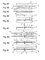
- a configuration of the system is shown in Fig. 9A .
- the optical fiber amplifier includes an optical isolator 53, an optical fiber 51 doped with erbium, a pumping laser 54 for radiating laser beam for excitation, a photo diode (PD) 52 for monitoring an output, and a filter 55 for adjusting a gain.
- the optical fiber amplifier can amplify a light output without converting an optical signal to an electrical signal, thus being indispensable to an optical communication network.
- a wavelength of the pumping laser 54 in a single mode fiber is 1.48 ⁇ m.
- the gain depends on a frequency as characteristic A of Fig. 9B . Therefore, a gain flattening filter (GFF) 55 having a characteristic reverse to characteristic A, namely having characteristic B, must be inserted into a transmission path after amplifying an optical output to flatten the gain as total characteristic C.
- GFF gain flattening filter
- the GFF 55 is usually inserted between fibers integrally, thus being formed in a module.
- the structure of the module is shown in Fig. 9C .
- Optical fibers 56, condensing lenses 57, and a GFF 58 are mounted and sealed into a metal case 59 after their optical axes are aligned.
- the optical fibers 56 are temporarily fixed to the metal case 59.
- the condensing lenses 57 for condensing light diffused from the optical fibers 56 and the GFF 58 are then mounted. Then, while optical signals radiated from the optical fiber 56 at an input side and output from the optical fiber 56 at an output side is measured by a power meter, their optical axes are aligned so as to obtain maximum optical signals. Then, the condensing lenses 57 and the GFF 58 are caulked and fixed to the metal case 59.
- optical axes i.e., an axis between the optical fiber 56 on the incoming side and the condensing lens 57, an axis between the condensing lens 57 and the gain flattening filter 58, an axis between the gain flattening filter and the condensing lens 57, and an axis between the condensing lens and the optical fiber 56 on the outgoing side must be aligned, thereby increasing cost.
- Japanese Patent No. 3175814 discloses a system for addressing the problem discussed above.
- a structure of the system is shown in Fig. 10A and Fig. 10B .
- a multi-layer film filter is inserted in an insertion groove crossing a built-in optical wave guide formed in a silicon substrate, thus providing a multiplexer/demultiplexer for wavelength division multiplexing (WDM).
- the filter system including a silicon substrate 31, a clad member 32, a wave guide 33 for input, a common port 331, a first wave guide 34 for output, a first output port 341, a second wave guide 35 for output, a second output port 351, an insertion groove 36 for a multi-layer film filter, and the multi-layer film filter 37.
- the filter system includes passages guiding light as the wave-guides and is formed in one plane.
- the filter insertion groove 36 crossing the wave guides allows respective optical axes of the wave guides 33, 35, and 34 not to be required to adjust.
- the filter insertion groove 36 having a width (W) a thickness (Df), and a width (Dg) satisfies, with the multi-layer film filter 37 having a camber of a curvature radius (R), the relation: R ⁇ W 2 / 8 ⁇ Dg - Df .
- the multi-layer film filter 37 can be securely fixed in the filter insertion groove 36 due to the camber of the filter.
- the built-in optical wave-guide forms an optical wave guide path, and a various filter is integrally inserted into the path.
- the multi-layer film filter 37 in this filter system necessarily has the camber of a curvature.
- the camber makes incidence angle to the multi-layer film filter shift largely due to its mounting displacement.
- the built-in optical wave guide upon being employed as the optical wave guide path, creates gaps formed inevitably between the wave guides 33, 35 and the multi-layer film filter 37 in the filter insertion groove 36. Light diffuses from wave-guides 33, 35 through the gaps and disappears. In addition, it is difficult to mechanically hold a component having a camber and to insert it into a micro groove.
- a similar construction but with fibres held in V-grooves of a main substrate via presser plates is also known in the art (see e.g. EP1008879 , US4958897 , or JP10300936 ).
- the groove receiving the filter can be tilted towards the upper surface of the substrate ( JP10300936 ).
- a separate holder can be provided (see e.g. JP09021912 or JP10307221 ) .
- filter receiving groove with one side wall being perpendicular to the substrate surface and the opposing side surface being oblique towards the substrate surface and guiding a fixing wedge abutting the filter to the side wall with the perpendicular orientation (see EP0908746 ).
- An optical filter module includes features of claim 1. Another optical filter module includes features of claim 2
- the multi-layer film filter can be securely fixed and mounted to an end surface of the optical fiber without relying on a camber of the filter.
- An upper plane substrate grapples the multi-layer film filter, so that the camber of the multi-layer film filter is corrected, and incident angles for the optical fiber and the multi-layer film filter are stabilized.
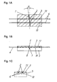
- Fig. 1A is a twin-core optical filter module in accordance with the exemplary embodiment of the present invention.
- Fig. 1B is a side view of the optical filter module, and
- Fig. 1C is a sectional view of the optical filter module.
- the module includes an insertion groove 1 for a multi-layer film filter, a multi-layer film filter 2, an upper plane substrate 3, an optical path 4, a lower plane substrate 5, and an optical adhesive 6.
- Respective main surfaces of the upper plane substrate 3 and the lower plane substrate 5 have V-shaped- grooves 10 and 11 formed therein.
- the multi-layer film filter 2 includes, for example, many dielectric films made of SiO 2 or Ta 2 O 5 and laminated on a resin substrate made of glass or polyimide.
- the upper plane substrate 3 and the lower plane substrate 5 are made of glass or silicon, and their linear expansion coefficients are preferably close to that of the optical path 4.
- a resin-based adhesive upon fixing the substrates, however, has elasticity to moderate stress caused by difference between the linear expansion coefficients.
- a photo-curing adhesive upon being used, is preferably made of light-transmittable material.
- the optical adhesive 6 has a refractive index equivalent to material of the optical path 4 so as to prevent light from dispersing from end surfaces of the optical path.
- refractive index of the optical adhesive 6 is preferably close to refractive index of 1.44 of the quartz glass.
- the optical path 4 is implemented, for exapmle, by an optical fiber, and the upper plane substrate 3 and the lower plane substrate 5 have V-grooves 10 and 11 for mounting and fixing the optical fiber, repectively.
- the V-grooves 10 and 11 have uniform depths and angles.
- the V-grooves 10 and 11 having certain depths and angles in the plane substrates 3 and 5 enables the plane substrates 3 and 5 to hold the optical fiber without displacement.
- the relation allows the center of the optical fiber to align at the surfaces of the plane substrates 3 and 5.
- a clad as the optical path of a glass-based optical fiber typically has a diameter of 125 ⁇ m. If each of the V-grooves 10 and 11 has a tip angle of 90 degrees a depth of about 180 ⁇ m, the upper and lower plane substrates 3, 5 grapple the optical fiber, thereby securely fixing the optical fiber.
- the V-grooves 10 and 11 formed in the upper and lower plane substrates 3, 5 do not necessarily have the same depth and angle.
- the angle and depth of the V-groove 11 formed in one plane substrate for grappling the optical fiber may be more than a projection amount of the optical fiber from the main surface of another plane substrate having the optical fiber mounted in the V-groove 10 formed in another substrate.
- This arrangement enables the optical fiber to be securely mounted and fixed onto the upper and lower plane substrates 3, 5.
- the V-grooves 10, 11 formed in the main surfaces of the plane substrates 3, 5 for grappling the optical fiber are larger than necessary, the upper plane substrate 3 does not function as a guide effectively in a manufacturing method described below. Therefore, the angles and depths of the V-grooves 10 and 11 ranges appropriately.
- the depth of the V-groove 11 formed in another plane substrate should be 10% longer than that of the V-groove 10.
- the filter insertion groove 1 formed in the lower plane substrate 5 is aligned by a predetermined angle ⁇ with respect to the optical fiber.
- the angle ⁇ prevents light incoming through the optical fiber to the multi-layer film filter 2 from being reflected, and depends on the wavelength of guided light.
- the angle ⁇ is preferably about 5 to 10 degrees.
- a core radius expansion fiber which includes a core partially expanded for confining and guiding the light, upon used as the optical fiber, can further reduce the coupling loss between the optical fiber and the multi-layer film filter 2.
- the multi-layer film filter 2 is inserted into the filter insertion groove 1 crossing optical path 4. Therefore, path of the optical fiber is divided by the filter insertion groove 1, and a gap having a width G identical to that of the filter insertion groove 1 is provided between end surfaces of the optical fibers via the multi-layer film filter 2.
- the core radius expansion fiber is represented by a thermally expanded core (TEC) fiber.
- the TEC fiber is a special fiber having a radius of a core substantially expanded by diffusing dope elements, such as GeO 2 , for controlling a refractive index of the core. The dope elements are diffused by heating a portion of a clad of the fiber.
- the TEC fiber can increase the spot size of the light from the end surfaces of the optical fibers.
- the filter insertion groove 1 preferably be machined and formed so as to cross a portion of the largest radius of the expanded core of the optical fiber.
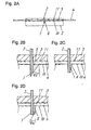
- the filter insertion groove 1 can have various shapes shown in Fig. 2B through Fig. 2D .
- one wall of the wall is shallow, and the other wall of the groove is deep at the bottom of the filter insertion groove 1.
- one wall of the groove is formed from the bottom of the filter insertion groove 1 to the main surface of the lower plane substrate 5 at a constant angle ⁇ 2.
- the bottom of the filter insertion groove 1 includes a flat portion.
- the bottom of the filter insertion groove 1 includes a flat portion, and a part of one wall of the groove slopes at a small angle ⁇ 4.
- the filter insertion groove 1 is formed with, for example, a diamond grindstone having its tip previously formed in the shape of the groove.
- the shape of the filter insertion groove 1 is the same as that of the tip of the diamond grindstone, so that the shape of the groove 1 largely depends on the accuracy of the diamond grindstone. If the width of the grindstone is 0.1mm or less, it is difficult to form the groove 1 due to a size of available diamond grain. If the width of the grindstone exceeds 0.1mm, the groove 1 is relatively easily formed.
- the filter insertion groove 1 has one wall sloping and another wall gentler than one wall, as shown in Fig. 2B to Fig. 2D , the multi-layer film filter 2 after insertion is prevented from tilting. While the filter insertion groove 1 is formed, the end surface of the upper plane substrate 3 having the fiber mounted thereon, i.e., a reference surface in a manufacturing method discussed below, receives a force in a direction that the diamond grindstone is pressed to the upper plane substrate 3 as the reference surface. This operation prevents the forming accuracy of the filter insertion groove 1 from degrading due to meandering of the diamond grindstone.
- the module includes two optical fibers, however, the module may include a multiple array having more fibers.
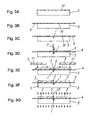
- the optical filter module according to the embodiment of the invention can be manufactured by various methods .
- the optical filter module includes an insertion groove 1 for a multi-layer film filter, a multi-layer film filter 2, an upper plane substrate 3, an optical fiber 4 as an optical path, a lower plane substrate 5, and an optical adhesive 6, a precise V-groove 10 formed in the main surface of the lower plane substrate 5, and a precise V-groove 11 formed in the main surface of the upper plane substrate 3.
- Reference numeral 12 denotes a light source, such as ultraviolet ray, or a heat source.
- the upper plane substrate 3 and the lower plane substrate 5 having precise V-grooves 10 and 11 in their main surfaces are prepared.
- the plane substrates 3 and 5 preferably are preferably made of material having a linear expansion coefficient equivalent to that of the optical fiber 4 mounted and fixed in a subsequent process, and being light-transmittable since the plane substrates 3 and 5 are fixed with a photo-curing adhesive.
- the optical fiber 4 is mounted and fixed on the lower plane substrate_5.
- the mounted portion of the optical fiber 4 is preferably a clad having no coating in consideration of mounting accuracy.
- the angle and depth of the V-groove 10 are determined so as to project the mounted optical fiber 4 from the main surface of the lower plane substrate 5.
- the optical fiber 4 projecting as a guide rail enables the upper plane substrate 3 to be positioned easily.
- the core radius expansion fiber may be used as the projecting optical fibers 4, thereby expanding a spot size at the end surfaces of the optical fibers 4 and reducing transmission loss or coupling loss between the optical fibers 4.
- the filter insertion groove 1 crossing the optical fibers 4 is formed in the main surface of the lower plane substrate 5 having the optical fiber 4 mounted thereon.
- the multi-layer film filter 2 is inserted into the filter insertion groove 1 in a subsequent process.
- the optical fibers 4 and the filter insertion groove 1 are crossed each other at a certain angle for preventing reflection of light at a surface of the multi-layer film filter 2.
- the angle of the crossing which depends on the wavelength of light, generally ranges from 5 through 10 degrees. If the core radius expansion fiber is used as the projecting optical fiber 4, the filter insertion groove 1 preferable crosses a portion having the largest radius of the core.
- the filter insertion groove 1 may be formed by grinding using a grindstone, or by powder machining, such as blasting.
- the grindstone for example, is formed in the shape of the groove and employs cBN or diamond as abrasive grain.
- the plane substrates may be made of silicon, thus allowing the groove to be formed by wet etching or dry etching.
- the cross section of the filter insertion groove 1 formed as discussed in the exemplary embodiment has its shape relatively freely formed by the grindstone.
- the filter insertion groove 1 is formed simultaneously to dividing of the optical fiber 4. For reducing roughness of the end surfaces of the cut and divided optical fiber 4, an abrasive grain size of the grindstone is as small as possible for machining.
- the filter insertion groove 1 is formed with a diamond grindstone according to the embodiment, and the diamond grain of #3000 or more, i.e., average diameter of 4 ⁇ m to 5 ⁇ m or more provides substantially-specular end surfaces of the optical fiber 4.
- the entire main surface of the lower plane substrate 5 is coated with the optical adhesive 6, and the multi-layer film filter 2 is inserted into the filter insertion groove 1 filled with the optical adhesive 6.
- the multi-layer film filter 2 has its size for having its upper portion project from the main surface of the lower plane substrate 5.
- the amount of the projected portion of the multi-layer film filter 2 is preferably at least one half or more of the thickness of the upper plane substrate.
- the optical adhesive 6 is put also into the filter insertion groove 1 formed in the previous process.
- the optical adhesive 6 has a refractive index equivalent to that of material of the core of the optical fiber 4, thereby reducing coupling loss between the fibers.
- the optical adhesive 6 may be cured with light, such as ultraviolet ray, or heating, however, be preferably cured with the light for reducing a manufacturing time.
- the upper plane substrates 3 having the V-grooves 11 in its main surfaces are moved from respective sides of the multi-layer film filter 2 projecting from the filter insertion groove 1.
- the optical fiber 4 projecting from the main surface of the lower plane substrate 5 functions as a guide rail.
- the multi-layer film filter 2 inserted into the filter insertion groove 1 is then grappled from both sides and fixed.
- one upper plane substrate 3 has a side surface contact a wall of the filter insertion groove 1, thereby mounting and fixing the inserted multi-layer film filter 2 along the wall of the filter insertion groove 1. This operation prevents the multi-layer film filter 2 from breaking when the filter is grappled with the other upper plane substrate 3.
- the projecting portion of the multi-layer film filter 2 is grappled. If the multi-layer film filter 2 cambers, the amount of the projecting portion thereof may be extended to have an area of the portion grappled with the upper plane substrate 3 enlarged to correct the camber.
- the multi-layer film filter 2 includes a substrate of glass can be prevented from breakage by stress since the glass has a large elastic coefficient.
- the angle and depth of the V-groove 11 formed in the main surface of upper plane substrate 3 are determined according to the amount of the projecting portion of the optical fiber 4. Tolerances of the angle and depth of the V-groove 11 against the amount of the projecting portion of the fiber reduces an effect as the guide rail of the optical fiber 4.
- the V-groove 11 smaller than the projecting amount of the optical fiber 4 reduces the effect as the guide rail and reliability. The reliability is reduced since the upper plane substrates 3 are mounted to the lower plane substrate 5 inclinedly about the optical fiber 4.
- Fig. 3G light, such as ultraviolet ray, is radiated or heat is applied from one side or both sides of the upper and lower plane substrates 3, 5 to cure and finish the optical filter module.
- the optical fiber 4 is mounted and fixed to the lower plane substrate 5, and is then cut simultaneously to forming of the filter insertion groove 1 in the processes discussed above. This process allows the optical axis of the end surfaces of the optical fiber 4 divided into two not to be required to align. Additionally, the cutting of the optical fiber 4 and the forming of the filter insertion groove 1 are simultaneously performed, thereby reducing manufacturing time.
- a precise V-groove 10 is formed in the main surface of the lower plane substrate 5, as shown in Fig. 4A .
- a filter insertion groove 1 crossing the precise V-groove 10 is then formed in the main surface of the lower plane substrate 5, as shown in Fig. 4B .
- the main surface of the lower plane substrate 5 is coated with an optical adhesive 6, and the multi-layer film filter 2 is inserted into the filter insertion groove 1.
- Fig. 4D previously divided optical fibers 4 are mounted and fixed along the V-groove 10 formed in main surface of the lower plane substrate 5.
- the multi-layer film filter 2 contacts a wall of the filter insertion groove 1, thus being prevented from breakage when the multi-layer film filter 2 is grappled with upper plane substrates 3.
- the optical fibers 4 have the end surfaces finished previously specularly, thus having a reduced transmission loss and coupling loss between the optical fibers 4.
- the end surfaces of the optical fibers 4 contact the main surface of the inserted multi-layer film filter 2, thereby further reducing the transmission loss and coupling loss between the optical fibers 4.
- Processes shown in Fig. 4E through Fig. 4G are the same as those of Fig. 3E through Fig. 3G , thus not being described.
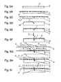
- plane substrates 3 and 5 having precise V-grooves 10 and 11 in their main surfaces, respectively, are prepared, as shown in Fig. 5A .
- the plane substrates 3 and 5 is preferably made of material having a linear expansion coefficient equivalent to that of an optical fiber 4 mounted and fixed in a subsequent process.
- the material may preferably be light-transmittable since the upper and lower plane substrates 3, 5 are fixed with a photo-curing adhesive.
- the optical fiber 4 is mounted and fixed in the precise V-groove 11 formed in the main surface of the upper plane substrate 3.
- the mounted portion of the optical fiber 4 may preferably includes a clad having no coating, such as resin, in consideration of the mounting accuracy
- the angle and depth of the V-groove 11 are determined to allow the mounted and fixed optical fiber 4 to project from the main surface of the lower plane substrate 5.
- the upper plane substrate 3 is thus easily positioned using the projecting optical fiber 4 as a guide rail.
- a core radius expansion fiber may be used as the projecting optical fiber 4, thereby expanding a spot size at the end surfaces of the optical fiber 4 and reducing the transmission loss or coupling loss between the optical fibers 4.
- the upper plane substrate 3 having optical fiber 4 mounted and fixed thereon in the previous process is cut and divided. If the core radius expansion fiber is used as the optical fiber 4, a portion having the largest radius of a core is cut. Finishing the cut surface of the optical fibers 4 in specular reduces the coupling loss between the optical fibers 4. When the cut surfaces are used as they are, the cutting condition must be considered. If the upper plane substrate 3 is cut with a diamond grindstone or the like, the grindstone has small abrasive grain size determined so that the end surface of cut optical fibers 4 is as specular as possible. According to this method, the diamond grindstone is used to form a filter insertion groove 1. The diamond grindstone includes diamond grain of #3000 or more, thereby allowing the end surfaces of the optical fibers 4 to be substantially specular.
- the filter insertion groove 1 crossing the precise V-groove 10 at a certain angle is formed in the main surface of the lower plane substrate 5.
- the crossing angle which is determined according to the wavelength of employed light, generally ranging from 5 to 10 degrees.
- the filter insertion groove 1 may be formed by grinding with a grindstone, or by powder machining, such as blasting.
- the grindstone for example, has the shape of the groove and employs cBN and diamond as abrasive grain.
- the plane substrates made of silicon enabling the groove 1 to be formed by wet etching or dry etching.
- the entire main surface of the lower plane substrate 5 is coated with an optical adhesive 6.
- the optical adhesive 6 is put also into the filter insertion groove 1 formed in the previous process.
- the optical adhesive 6 has a refractive index equivalent to that of material of a core of the optical fibers 4, thereby reducing the coupling loss between the optical fibers 4.
- the optical adhesive 6 is cured with light, such as ultraviolet ray, or heating. The curing with the light is more advantageous for reducing manufacturing time.
- the multi-layer film filter 2 is inserted into the filter insertion groove 1 filled with the optical adhesive 6.
- the multi-layer film filter 2 has its size to allowing the upper part of the inserted multi-layer film filter 2 to project from the main surface of the lower plane substrate 5.
- the amount a projecting portion of the multi-layer film filter 2 is preferably at least one half or more of the thickness of the upper plane substrate 3.
- the upper plane substrates 3 having the V-groove 11 in the main surface are moved from respective sides of the multi-layer film filter 2 projecting from the filter insertion groove 1.
- the optical fiber 4 projecting from the main surface of the lower plane substrate 5 functions as a guide rail.
- the multi-layer film filter 2 inserted into the filter insertion groove 1 is grappled from their both sides and fixed.
- one upper plane substrate 3 is mounted so that a side surface of the upper plane substrate 3 is aligned to a wall of the filter insertion groove 1, thereby mounting and fixing the inserted multi-layer film filter 2 on the wall of the filter insertion groove 1. This operation prevents the multi-layer film filter 2 from breakage when the filter is grappled with the other upper plane substrate 3.
- the multi-layer film filter 2 is grappled at its projecting potion. If the multi-layer film filter 2 cambers, the amount of its projecting portion has an enlarged area of a portion grappled by the upper plane substrate 3 to correct the camber.
- the multi-layer film filter 2 including a substrate of glass can be prevented from breakage due to stress since the glass has a large elastic coefficient.
- the angle and depth of the V-groove 11 formed in the main surface of each upper plane substrate 3 are determined according to the amount of the projecting portion of the optical fiber 4. Tolerances of the angle and depth of the V-groove for the projecting amount reduces an effect as the guide rail of the optical fiber 4.
- the V-groove 11 smaller than the projecting amount of the optical fiber 4 reduces the effect as the guide rail and reliability The reliability may is reduced since the upper plane substrates 3 are mounted to the lower plane substrate 5 inclinedly about the optical fiber 4.
- Fig. 5I light 12, such as ultraviolet ray, is radiated, or heat 12 is applied from one side or both sides of the upper and lower plane substrates 3, 5 to cure and finish the optical filter module.
- the upper plane substrates 3 previously having the optical fibers 4 mounted thereon are prepared as discussed above. This preparation enables the process of applying the optical adhesive 6, the process of inserting the multi-layer film filter 2, and the process of grappling the multi-layer film filter 2 by the upper plane substrates 3 to be executed continuously, and facilitates manufacturing control.
- a precise V-groove 11 is formed in the main surface of an upper plane substrate 3, as shown in Fig. 6A .
- the upper plane substrate 3 is then divided into two, as shown in Fig. 6B , and two optical fibers 4 are mounted to the respective upper plane substrates 3 divided so that an end surface of each optical fiber 4 fits to an end surface of each upper plane substrate 3.
- a special processing such as specular finish or spherical polishing, can be applied to the end surfaces of the optical fibers 4, so that the coupling loss between the optical fibers 4 can advantageously reduced.
- the subsequent processes shown in Fig. 6C through Fig. 6I are the same as those of Fig. 5C through Fig. 5I , and their descriptions are therefore omitted.
- a filter insertion groove 1 crossing a precise V-groove 10 at a certain angle is formed in the main surface of the lower plane substrate 5.
- Processes shown in Fig. 7A through Fig. 7D are the same as those of Fig. 5A through Fig. 5D .
- Fig. 7E one upper plane substrate 3 having the optical fiber 4 mounted thereon is guided by the precise V-groove 10 formed in the main surface of the lower plane substrate 5 and contacts the main surface of the lower plane substrate 5.
- the upper plane substrate 3 is positioned and fixed so that the end surface of the optical fiber 4 mounted on the upper plane substrate 3 contacts a wall of the filter insertion groove 1.
- an optical adhesive 6 is then applied to the main surface of the lower plane substrate 5 before having upper plane substrate 3 mounted thereon. At this moment, the optical adhesive 6 is also put into the filter insertion groove 1.
- a multi-layer film filter 2 is then inserted into the filter insertion groove 1 to contact the end surface of the fixed upper plane substrate 3. The multi-layer film filter 2 contacts the filter insertion groove 1 and the end surface of the upper plane substrate 3, thus being prevented from breaking when the filter is grappled with the other upper plane substrate 3.
- the other upper plane substrate 3 is then disposed on a portion of the main surface of the lower plane substrate 5 having no upper plane substrate 3 mounted thereon.
- the upper plane substrate 3 moves so as to make the optical fiber 4 projecting from the main surface of the upper plane substrate 3 slide along the precise V-groove formed in the main surface of the lower plane substrate 5. Then, the substrate 3 abuts on the multi-layer film filter 2 inserted into the filter insertion groove 1 to grapple and fix the filter 2.
- Fig. 7I finally, light 12, such as ultraviolet ray, is radiated, or heat 12 is applied from one side or both sides of the upper and lower plane substrates 3, 5 to cure and finish the optical filter module.
- the inserted multi-layer film filter 2 is fixed on the upper plane substrate 3 and the wall of the filter insertion groove 1, thus being prevented from breaking. Since one upper plane substrate 3 is previously fixed, the other upper plane substrate 3 is easily positioned.
- FIG. 8A through Fig. 8I Another manufacturing method shown in Fig. 8A through Fig. 8I includes processes shown in Fig. 8A through Fig. 8C which are the same as those in the manufacturing method shown in Figs. 7A to 7C .
- Fig. 8D upper plane substrate 3 having an optical fiber 4 mounted thereon is mounted and fixed on the main surface of the lower plane substrate 5.
- the lower plane substrate 5 is mounted and fixed so that the optical fiber 4 projecting from the main surface of the upper plane substrate 3 is taken, as a guide rail, along a precise V-groove 10 formed in the main surface of the lower plane substrate 5.
- a filter insertion groove 1 is formed in the main surface of the lower plane substrate 5 along an end surface of the mounted upper plane substrate 3 at a certain angle with respect to a precise V-groove 11 formed in the main surface.
- the filter insertion groove 1 is formed after one upper plane substrate 3 is mounted and fixed on the main surface of the lower plane substrate 5, thus allowing the upper plane substrate 3 to be easily positioned.
- the method shown in Fig. 8A through Fig. 8E can be applicable to the manufacturing methods shown in Fig. 3A through Fig. 3G and shown in Fig. 4A through Fig. 4G .
- the optical fiber 4 is mounted on the lower plane substrate 5, then one upper plane substrate 3 having the precise V-groove 11 in its main surface is mounted and fixed.
- the filter insertion groove 1 is formed in the lower plane substrate 5 with reference to an end surface of the upper plane substrate 3.
- the subsequent processes shown in Fig. 8F through Fig. 8I are the same as those in the manufacturing method shown in Figs. 7F to 7I , and therefore, their explanations are omitted.
- precise V-grooves are formed in main surfaces of upper and lower plane substrates, and an optical fiber is mounted in the V-grooves, thereby allowing the optical fiber to me mounted easily on the main surface.
- the precise V-groove formed in the main surface of one plane substrate functions as a guide rail, the other plane substrate grapples a multi-layer film filter inserted into an insertion groove.
- This arrangement provides an optical filter module in which shape deformation, such as camber, of the multi-layer film filter does not affect, the upper plane substrate is easily positioned, and adjustment of an optical axis is not required.
Landscapes
- Physics & Mathematics (AREA)
- General Physics & Mathematics (AREA)
- Optics & Photonics (AREA)
- Optical Couplings Of Light Guides (AREA)
- Mechanical Coupling Of Light Guides (AREA)
- Light Guides In General And Applications Therefor (AREA)
Claims (5)
- Optisches Filtermodul, das umfasst:ein Filter (2);eine erste und eine zweite Lichtleitfaser (4), die jeweils Querschnitte haben, die einander an jeweiligen Seiten des Filters (2) zugewandt sind;ein erstes Substrat (5), das eine Fläche hat, in der eine erste Nut (10) und eine Filtereinführnut (1) ausgebildet sind, wobei in der ersten Nut (10) die erste und die zweite Lichtleitfaser (4) gehalten werden, und in der Filtereinführnut (1) das Filter (2) befestigt ist und sie die erste Nut (10) schneidet;ein zweites Substrat (3), das die erste Lichtleitfaser (4) mit dem ersten Substrat (1) festhält, wobei in dem zweiten Substrat (3) eine zweite Nut (11) ausgebildet ist, um die erste Lichtleitfaser (4) darin aufzunehmen; undein drittes Substrat (3), das die zweite Lichtleitfaser (4) mit dem ersten Substrat (5) festhält, das Filter (2) mit dem zweiten Substrat (3) festhält und in dem eine dritte Nut (11) ausgebildet ist, in der die zweite Lichtleitfaser (4) aufgenommen wird.dadurch gekennzeichnet, dass:die Filtereinführnut (1) besteht aus:einer ersten Seitenwand (2), an der das Filter anliegt und die im Wesentlichen senkrecht zu der Oberfläche des ersten Substrats (5) ist; undeiner zweiten Seitenwand (2), die der ersten Seitenwand (2) gegenüberliegt und in einem Winkel (θ2, 64) in Bezug auf die Oberfläche des ersten Substrats (5) ausgebildet ist.
- Optisches Filtermodul, das umfasst:ein Filter (2);eine erste und eine zweite Lichtleitfaser (4), die jeweils Querschnitte haben, die einander an jeweiligen Seiten des Filters (2) zugewandt sind;ein erstes Substrat (5), das eine Fläche hat, in der eine erste Nut (10) und eine Filtereinführnut (1) ausgebildet sind, wobei in der ersten Nut (10) die erste und die zweite Lichtleitfaser (4) gehalten werden, und in der Filtereinführnut (1) das Filter (2) befestigt ist und sie die erste Nut (10) schneidet;ein zweites Substrat (3), das die erste Lichtleitfaser (4) mit dem ersten Substrat (1) festhält, wobei in dem zweiten Substrat (3) eine zweite Nut (11) ausgebildet ist, um die erste Lichtleitfaser (4) darin aufzunehmen; undein drittes Substrat (3), die die zweite Lichtleitfaser (4) mit dem ersten Substrat (5) festhält, das Filter (2) mit dem zweiten Substrat (3) festhält und in dem eine dritte Nut (11) ausgebildet ist, in der die zweite Lichtleitfaser (4) aufgenommen wird.dadurch gekennzeichnet, dass:die Filtereinführnut (1) besteht aus:einer ersten Seitenwand, die im Wesentlichen senkrecht zu der Oberfläche des ersten Substrats (5) ist;einer zweiten Seitenwand, die der ersten Wand gegenüberliegt und in einem Winkel (θ2, θ4) in Bezug auf die Oberfläche des ersten Substrats (5) ausgebildet ist; undeinem flachen Bodenabschnitt, der die erste und die zweite Seitenwand verbindet;wobei das Filter (2) an der ersten Seitenwand und dem flachen Bodenabschnitt der Filtereinführnut (1) anliegt.
- Optisches Filtermodul nach Anspruch 1 oder 2, wobei die erste und die zweite Lichtleitfaser (4) Fasern zum Aufweiten des Kernradius umfassen.
- Optisches Filtermodul nach Anspruch 1 oder 2, wobei jeweilige Endflächen der ersten und der zweiten Lichtleitfaser (4), die dem Filter zugewandt sind, aufgeweitete Radien von Kernen derselben aufweisen.
- Optisches Filtermodul nach Anspruch 1 oder 2, wobei das erste bis dritte Substrat (3, 5) und die erste sowie die zweite Lichtleitfaser (4) über einen lichthärtenden Klebstoff oder einen wärmehärtenden Klebstoff verbunden sind.
Applications Claiming Priority (3)
| Application Number | Priority Date | Filing Date | Title |
|---|---|---|---|
| JP2001308310 | 2001-10-04 | ||
| JP2001308310A JP2003114335A (ja) | 2001-10-04 | 2001-10-04 | 光フィルタモジュールおよびその製造方法 |
| PCT/JP2002/010258 WO2003032030A1 (en) | 2001-10-04 | 2002-10-02 | Optical filter module and manufacturing method thereof |
Publications (3)
| Publication Number | Publication Date |
|---|---|
| EP1434066A1 EP1434066A1 (de) | 2004-06-30 |
| EP1434066A4 EP1434066A4 (de) | 2005-05-11 |
| EP1434066B1 true EP1434066B1 (de) | 2012-04-11 |
Family
ID=19127643
Family Applications (1)
| Application Number | Title | Priority Date | Filing Date |
|---|---|---|---|
| EP02800727A Expired - Lifetime EP1434066B1 (de) | 2001-10-04 | 2002-10-02 | Optisches filtermodul |
Country Status (6)
| Country | Link |
|---|---|
| US (1) | US7172344B2 (de) |
| EP (1) | EP1434066B1 (de) |
| JP (1) | JP2003114335A (de) |
| CN (1) | CN1252497C (de) |
| TW (1) | TW579442B (de) |
| WO (1) | WO2003032030A1 (de) |
Cited By (1)
| Publication number | Priority date | Publication date | Assignee | Title |
|---|---|---|---|---|
| US12158610B2 (en) | 2019-10-25 | 2024-12-03 | Commscope Technologies Llc | Integrated optical wavelength division multiplexing devices |
Families Citing this family (9)
| Publication number | Priority date | Publication date | Assignee | Title |
|---|---|---|---|---|
| JP2003114334A (ja) * | 2001-10-04 | 2003-04-18 | Matsushita Electric Ind Co Ltd | 光フィルタモジュールおよびその製造方法 |
| FR2842915B1 (fr) * | 2002-07-26 | 2004-10-08 | Atmel Grenoble Sa | Procede et dispositif de positionnement d'un composant optique entre deux fibres optiques |
| JP4682111B2 (ja) * | 2006-09-14 | 2011-05-11 | 富士通株式会社 | 導波路型光デバイス及びその製造方法 |
| FR2936739B1 (fr) | 2008-10-03 | 2013-03-22 | Bic Soc | Instrument d'ecriture comprenant un organe d'extremite monte par emmanchement. |
| JP6810076B2 (ja) * | 2018-03-13 | 2021-01-06 | 日本電信電話株式会社 | ファイバモジュール |
| WO2022015669A1 (en) * | 2020-07-14 | 2022-01-20 | Nlight, Inc. | Opto-mechanical mounting for optical components |
| CN112903102B (zh) * | 2021-01-21 | 2023-02-10 | 华中科技大学 | 一种芯片级光谱仪及其制备方法 |
| CN113885154A (zh) * | 2021-09-26 | 2022-01-04 | 武汉光迅科技股份有限公司 | 一种光学滤片组件及制作方法 |
| US12130470B2 (en) * | 2021-10-25 | 2024-10-29 | Globalfoundries U.S. Inc. | PIC die and package with multiple level and multiple depth connections of fibers to on-chip optical components |
Citations (5)
| Publication number | Priority date | Publication date | Assignee | Title |
|---|---|---|---|---|
| US4958897A (en) * | 1988-06-29 | 1990-09-25 | The Furukawa Electric Co., Ltd. | Thin film optical component for use in optical transmission lines and method of manufacturing the same |
| JPH0921912A (ja) * | 1995-07-05 | 1997-01-21 | Furukawa Electric Co Ltd:The | 誘電体多層膜フィルタおよびその作製方法および誘電体多層膜フィルタの光導波路への挿入構造 |
| JPH10300936A (ja) * | 1997-04-24 | 1998-11-13 | Matsushita Electric Ind Co Ltd | 光学フィルタ内蔵光通信部品およびその製造方法 |
| EP0908746A2 (de) * | 1997-10-06 | 1999-04-14 | Fujitsu Limited | Optische Wellenlängenmultiplex Anordnung und ihrer Herstellungsverfahren |
| EP1008879A2 (de) * | 1998-12-09 | 2000-06-14 | Fujitsu Limited | Muffenanordnung und optisches Modul |
Family Cites Families (19)
| Publication number | Priority date | Publication date | Assignee | Title |
|---|---|---|---|---|
| US4639074A (en) * | 1984-06-18 | 1987-01-27 | At&T Bell Laboratories | Fiber-waveguide self alignment coupler |
| JPS6434604U (de) | 1987-08-25 | 1989-03-02 | ||
| JPH0215203A (ja) * | 1988-07-04 | 1990-01-18 | Nippon Telegr & Teleph Corp <Ntt> | 光ファイバ型光分波器 |
| JPH02284103A (ja) | 1989-04-26 | 1990-11-21 | Furukawa Electric Co Ltd:The | 光部品及びその製造方法 |
| JPH0634837A (ja) | 1992-07-15 | 1994-02-10 | Sumitomo Electric Ind Ltd | 光部品 |
| JPH075346A (ja) | 1993-06-18 | 1995-01-10 | Sumitomo Osaka Cement Co Ltd | 光素子用光ファイバ固定具および光素子に光ファイバを接続固定する方法 |
| JPH07281049A (ja) | 1994-04-11 | 1995-10-27 | Fuji Elelctrochem Co Ltd | ファイバ集積型光部品の製造方法 |
| JPH08184712A (ja) | 1995-01-06 | 1996-07-16 | Furukawa Electric Co Ltd:The | 光ファイバ型光フィルタ |
| JPH08211228A (ja) | 1995-02-06 | 1996-08-20 | Furukawa Electric Co Ltd:The | フィルタ入り光ファイバ |
| JP3500765B2 (ja) | 1995-04-25 | 2004-02-23 | 住友電気工業株式会社 | 光フィルタの製造方法 |
| JP3175814B2 (ja) | 1995-10-09 | 2001-06-11 | 日本電信電話株式会社 | 導波形光素子及びその製造方法 |
| JPH1048439A (ja) | 1996-08-02 | 1998-02-20 | Japan Aviation Electron Ind Ltd | 光学フィルタ |
| JPH10307221A (ja) * | 1997-05-09 | 1998-11-17 | Hitachi Ltd | 半導体光結合装置及びその組立方法 |
| JP3520763B2 (ja) | 1998-04-21 | 2004-04-19 | 三菱マテリアル株式会社 | チップ型サージアブソーバの製造方法 |
| JPH11305078A (ja) * | 1998-04-27 | 1999-11-05 | Oki Electric Ind Co Ltd | 光送受信モジュール |
| JP2000249874A (ja) * | 1999-02-25 | 2000-09-14 | Nhk Spring Co Ltd | 光送受信モジュール |
| JP2000275479A (ja) * | 1999-03-26 | 2000-10-06 | Ngk Insulators Ltd | 複数段v溝を有するv溝基板及びその製造方法 |
| US6535655B1 (en) * | 2000-01-18 | 2003-03-18 | Corning Incorporated | Fiberoptic polarizer and method of making the same |
| JP2002189151A (ja) * | 2000-10-11 | 2002-07-05 | Matsushita Electric Ind Co Ltd | 光受信モジュール、光送受信モジュール及び製造方法 |
-
2001
- 2001-10-04 JP JP2001308310A patent/JP2003114335A/ja active Pending
-
2002
- 2002-10-02 CN CNB028029011A patent/CN1252497C/zh not_active Expired - Fee Related
- 2002-10-02 TW TW091122722A patent/TW579442B/zh not_active IP Right Cessation
- 2002-10-02 US US10/381,506 patent/US7172344B2/en not_active Expired - Fee Related
- 2002-10-02 WO PCT/JP2002/010258 patent/WO2003032030A1/ja not_active Ceased
- 2002-10-02 EP EP02800727A patent/EP1434066B1/de not_active Expired - Lifetime
Patent Citations (5)
| Publication number | Priority date | Publication date | Assignee | Title |
|---|---|---|---|---|
| US4958897A (en) * | 1988-06-29 | 1990-09-25 | The Furukawa Electric Co., Ltd. | Thin film optical component for use in optical transmission lines and method of manufacturing the same |
| JPH0921912A (ja) * | 1995-07-05 | 1997-01-21 | Furukawa Electric Co Ltd:The | 誘電体多層膜フィルタおよびその作製方法および誘電体多層膜フィルタの光導波路への挿入構造 |
| JPH10300936A (ja) * | 1997-04-24 | 1998-11-13 | Matsushita Electric Ind Co Ltd | 光学フィルタ内蔵光通信部品およびその製造方法 |
| EP0908746A2 (de) * | 1997-10-06 | 1999-04-14 | Fujitsu Limited | Optische Wellenlängenmultiplex Anordnung und ihrer Herstellungsverfahren |
| EP1008879A2 (de) * | 1998-12-09 | 2000-06-14 | Fujitsu Limited | Muffenanordnung und optisches Modul |
Cited By (1)
| Publication number | Priority date | Publication date | Assignee | Title |
|---|---|---|---|---|
| US12158610B2 (en) | 2019-10-25 | 2024-12-03 | Commscope Technologies Llc | Integrated optical wavelength division multiplexing devices |
Also Published As
| Publication number | Publication date |
|---|---|
| EP1434066A1 (de) | 2004-06-30 |
| US7172344B2 (en) | 2007-02-06 |
| CN1473277A (zh) | 2004-02-04 |
| EP1434066A4 (de) | 2005-05-11 |
| JP2003114335A (ja) | 2003-04-18 |
| WO2003032030A1 (en) | 2003-04-17 |
| US20040027705A1 (en) | 2004-02-12 |
| TW579442B (en) | 2004-03-11 |
| CN1252497C (zh) | 2006-04-19 |
Similar Documents
| Publication | Publication Date | Title |
|---|---|---|
| US4958897A (en) | Thin film optical component for use in optical transmission lines and method of manufacturing the same | |
| KR101258725B1 (ko) | 얇은 soi cmos 광 집적회로의 광대역 광 커플링 | |
| EP0642045A1 (de) | Hybrides optisches IC mit optischen Achsen auf verschiedenen Ebenen | |
| GB2329259A (en) | Optical device and method for producing such a device | |
| JP2002189151A (ja) | 光受信モジュール、光送受信モジュール及び製造方法 | |
| EP1434066B1 (de) | Optisches filtermodul | |
| EP1146359A2 (de) | Faseroptischer Polarisator und Verfahren zu dessen Herstellung | |
| US7447400B2 (en) | Optical waveguide substrate and method of fabricating the same | |
| US6775459B2 (en) | Variable optical attenuator | |
| JP2003294992A (ja) | 光デバイス | |
| KR20050092126A (ko) | 작은 형태 인자를 가진 렌즈형 광섬유 및 그 제조방법 | |
| EP0846966A2 (de) | Optischer Wellenleiter | |
| US7044649B2 (en) | Optical filter module, and manufacturing method thereof | |
| JPH0634837A (ja) | 光部品 | |
| CA2333456A1 (en) | Assembly of optical component and optical fibre | |
| JP3914450B2 (ja) | 光デバイス及びその製造方法 | |
| EP1816501B1 (de) | Optische Demultiplex-Vorrichtung | |
| JP4340210B2 (ja) | 光学部品およびその製造方法 | |
| US7039279B2 (en) | Optical filter module and manufacturing method thereof | |
| JP2000009953A (ja) | 波長分波器とこの波長分波器を備えた光送受信モジュール | |
| JPH08248254A (ja) | 光ファイバの接続方法 | |
| JP4140094B2 (ja) | 光導波路素子及びその製造方法 | |
| EP0948150A2 (de) | Lichtüberwachungsvorrichtung mit einfacher Struktur | |
| JPH0627335A (ja) | 光導波路デバイス | |
| JPH0484110A (ja) | 光制御素子内蔵型光伝送用部材 |
Legal Events
| Date | Code | Title | Description |
|---|---|---|---|
| PUAI | Public reference made under article 153(3) epc to a published international application that has entered the european phase |
Free format text: ORIGINAL CODE: 0009012 |
|
| 17P | Request for examination filed |
Effective date: 20030513 |
|
| AK | Designated contracting states |
Kind code of ref document: A1 Designated state(s): AT BE BG CH CY CZ DE DK EE ES FI FR GB GR IE IT LI LU MC NL PT SE SK TR |
|
| A4 | Supplementary search report drawn up and despatched |
Effective date: 20050329 |
|
| RIC1 | Information provided on ipc code assigned before grant |
Ipc: 7G 02B 6/34 A |
|
| 17Q | First examination report despatched |
Effective date: 20080228 |
|
| RAP1 | Party data changed (applicant data changed or rights of an application transferred) |
Owner name: PANASONIC CORPORATION |
|
| REG | Reference to a national code |
Ref country code: DE Ref legal event code: R079 Ref document number: 60242656 Country of ref document: DE Free format text: PREVIOUS MAIN CLASS: G02B0006340000 Ipc: G02B0006293000 Ref country code: DE Ref legal event code: R079 Ref document number: 60242656 Country of ref document: DE Free format text: PREVIOUS MAIN CLASS: G02B0006000000 Ipc: G02B0006293000 |
|
| RIC1 | Information provided on ipc code assigned before grant |
Ipc: G02B 6/293 20060101AFI20110906BHEP |
|
| RTI1 | Title (correction) |
Free format text: OPTICAL FILTER MODULE |
|
| GRAP | Despatch of communication of intention to grant a patent |
Free format text: ORIGINAL CODE: EPIDOSNIGR1 |
|
| RBV | Designated contracting states (corrected) |
Designated state(s): DE FR GB |
|
| GRAS | Grant fee paid |
Free format text: ORIGINAL CODE: EPIDOSNIGR3 |
|
| GRAA | (expected) grant |
Free format text: ORIGINAL CODE: 0009210 |
|
| AK | Designated contracting states |
Kind code of ref document: B1 Designated state(s): DE FR GB |
|
| REG | Reference to a national code |
Ref country code: GB Ref legal event code: FG4D |
|
| REG | Reference to a national code |
Ref country code: DE Ref legal event code: R096 Ref document number: 60242656 Country of ref document: DE Effective date: 20120531 |
|
| PLBE | No opposition filed within time limit |
Free format text: ORIGINAL CODE: 0009261 |
|
| STAA | Information on the status of an ep patent application or granted ep patent |
Free format text: STATUS: NO OPPOSITION FILED WITHIN TIME LIMIT |
|
| 26N | No opposition filed |
Effective date: 20130114 |
|
| REG | Reference to a national code |
Ref country code: DE Ref legal event code: R097 Ref document number: 60242656 Country of ref document: DE Effective date: 20130114 |
|
| PGFP | Annual fee paid to national office [announced via postgrant information from national office to epo] |
Ref country code: FR Payment date: 20141022 Year of fee payment: 13 Ref country code: GB Payment date: 20141021 Year of fee payment: 13 Ref country code: DE Payment date: 20141022 Year of fee payment: 13 |
|
| REG | Reference to a national code |
Ref country code: DE Ref legal event code: R119 Ref document number: 60242656 Country of ref document: DE |
|
| GBPC | Gb: european patent ceased through non-payment of renewal fee |
Effective date: 20151002 |
|
| PG25 | Lapsed in a contracting state [announced via postgrant information from national office to epo] |
Ref country code: DE Free format text: LAPSE BECAUSE OF NON-PAYMENT OF DUE FEES Effective date: 20160503 Ref country code: GB Free format text: LAPSE BECAUSE OF NON-PAYMENT OF DUE FEES Effective date: 20151002 |
|
| REG | Reference to a national code |
Ref country code: FR Ref legal event code: ST Effective date: 20160630 |
|
| PG25 | Lapsed in a contracting state [announced via postgrant information from national office to epo] |
Ref country code: FR Free format text: LAPSE BECAUSE OF NON-PAYMENT OF DUE FEES Effective date: 20151102 |