EP1434285A2 - Organisches, halbleitendes Polymer und ein organischer Dünnschichttransistor - Google Patents
Organisches, halbleitendes Polymer und ein organischer Dünnschichttransistor Download PDFInfo
- Publication number
- EP1434285A2 EP1434285A2 EP03257774A EP03257774A EP1434285A2 EP 1434285 A2 EP1434285 A2 EP 1434285A2 EP 03257774 A EP03257774 A EP 03257774A EP 03257774 A EP03257774 A EP 03257774A EP 1434285 A2 EP1434285 A2 EP 1434285A2
- Authority
- EP
- European Patent Office
- Prior art keywords
- organic
- thin film
- formula
- film transistor
- polymer
- Prior art date
- Legal status (The legal status is an assumption and is not a legal conclusion. Google has not performed a legal analysis and makes no representation as to the accuracy of the status listed.)
- Withdrawn
Links
Images


Classifications
-
- H—ELECTRICITY
- H10—SEMICONDUCTOR DEVICES; ELECTRIC SOLID-STATE DEVICES NOT OTHERWISE PROVIDED FOR
- H10K—ORGANIC ELECTRIC SOLID-STATE DEVICES
- H10K85/00—Organic materials used in the body or electrodes of devices covered by this subclass
- H10K85/10—Organic polymers or oligomers
- H10K85/111—Organic polymers or oligomers comprising aromatic, heteroaromatic, or aryl chains, e.g. polyaniline, polyphenylene or polyphenylene vinylene
- H10K85/113—Heteroaromatic compounds comprising sulfur or selene, e.g. polythiophene
-
- C—CHEMISTRY; METALLURGY
- C08—ORGANIC MACROMOLECULAR COMPOUNDS; THEIR PREPARATION OR CHEMICAL WORKING-UP; COMPOSITIONS BASED THEREON
- C08G—MACROMOLECULAR COMPOUNDS OBTAINED OTHERWISE THAN BY REACTIONS ONLY INVOLVING UNSATURATED CARBON-TO-CARBON BONDS
- C08G75/00—Macromolecular compounds obtained by reactions forming a linkage containing sulfur with or without nitrogen, oxygen, or carbon in the main chain of the macromolecule
- C08G75/32—Polythiazoles; Polythiadiazoles
-
- C—CHEMISTRY; METALLURGY
- C08—ORGANIC MACROMOLECULAR COMPOUNDS; THEIR PREPARATION OR CHEMICAL WORKING-UP; COMPOSITIONS BASED THEREON
- C08G—MACROMOLECULAR COMPOUNDS OBTAINED OTHERWISE THAN BY REACTIONS ONLY INVOLVING UNSATURATED CARBON-TO-CARBON BONDS
- C08G61/00—Macromolecular compounds obtained by reactions forming a carbon-to-carbon link in the main chain of the macromolecule
- C08G61/12—Macromolecular compounds containing atoms other than carbon in the main chain of the macromolecule
- C08G61/122—Macromolecular compounds containing atoms other than carbon in the main chain of the macromolecule derived from five- or six-membered heterocyclic compounds, other than imides
- C08G61/123—Macromolecular compounds containing atoms other than carbon in the main chain of the macromolecule derived from five- or six-membered heterocyclic compounds, other than imides derived from five-membered heterocyclic compounds
-
- C—CHEMISTRY; METALLURGY
- C08—ORGANIC MACROMOLECULAR COMPOUNDS; THEIR PREPARATION OR CHEMICAL WORKING-UP; COMPOSITIONS BASED THEREON
- C08G—MACROMOLECULAR COMPOUNDS OBTAINED OTHERWISE THAN BY REACTIONS ONLY INVOLVING UNSATURATED CARBON-TO-CARBON BONDS
- C08G61/00—Macromolecular compounds obtained by reactions forming a carbon-to-carbon link in the main chain of the macromolecule
- C08G61/12—Macromolecular compounds containing atoms other than carbon in the main chain of the macromolecule
- C08G61/122—Macromolecular compounds containing atoms other than carbon in the main chain of the macromolecule derived from five- or six-membered heterocyclic compounds, other than imides
- C08G61/123—Macromolecular compounds containing atoms other than carbon in the main chain of the macromolecule derived from five- or six-membered heterocyclic compounds, other than imides derived from five-membered heterocyclic compounds
- C08G61/126—Macromolecular compounds containing atoms other than carbon in the main chain of the macromolecule derived from five- or six-membered heterocyclic compounds, other than imides derived from five-membered heterocyclic compounds with a five-membered ring containing one sulfur atom in the ring
-
- H—ELECTRICITY
- H01—ELECTRIC ELEMENTS
- H01B—CABLES; CONDUCTORS; INSULATORS; SELECTION OF MATERIALS FOR THEIR CONDUCTIVE, INSULATING OR DIELECTRIC PROPERTIES
- H01B1/00—Conductors or conductive bodies characterised by the conductive materials; Selection of materials as conductors
- H01B1/06—Conductors or conductive bodies characterised by the conductive materials; Selection of materials as conductors mainly consisting of other non-metallic substances
- H01B1/12—Conductors or conductive bodies characterised by the conductive materials; Selection of materials as conductors mainly consisting of other non-metallic substances organic substances
- H01B1/124—Intrinsically conductive polymers
- H01B1/127—Intrinsically conductive polymers comprising five-membered aromatic rings in the main chain, e.g. polypyrroles, polythiophenes
-
- H—ELECTRICITY
- H10—SEMICONDUCTOR DEVICES; ELECTRIC SOLID-STATE DEVICES NOT OTHERWISE PROVIDED FOR
- H10K—ORGANIC ELECTRIC SOLID-STATE DEVICES
- H10K10/00—Organic devices specially adapted for rectifying, amplifying, oscillating or switching; Organic capacitors or resistors having potential barriers
- H10K10/40—Organic transistors
- H10K10/46—Field-effect transistors, e.g. organic thin-film transistors [OTFT]
- H10K10/462—Insulated gate field-effect transistors [IGFETs]
- H10K10/466—Lateral bottom-gate IGFETs comprising only a single gate
-
- H—ELECTRICITY
- H10—SEMICONDUCTOR DEVICES; ELECTRIC SOLID-STATE DEVICES NOT OTHERWISE PROVIDED FOR
- H10K—ORGANIC ELECTRIC SOLID-STATE DEVICES
- H10K71/00—Manufacture or treatment specially adapted for the organic devices covered by this subclass
- H10K71/10—Deposition of organic active material
- H10K71/12—Deposition of organic active material using liquid deposition, e.g. spin coating
Definitions
- the present invention relates to a novel organic semiconductor polymer and an organic transistor using the same, and more particularly to a composite-structured polythienylthiazole derivative in which thiazole rings having a high electron affinity, i.e. n-type semiconductor properties, are incorporated with thiophene units having p-type semiconductor properties, thereby exhibiting both p-type and n-type semiconductor properties.
- organic thin film transistors employing a polythiophene-based material, e.g., P3HT(Poly(3-hexylthiophene) or F8T2 (a copolymer consisting of dioctylfluorene and bithiophene (ratio of 8: 2)).
- P3HT Poly(3-hexylthiophene) or F8T2 (a copolymer consisting of dioctylfluorene and bithiophene (ratio of 8: 2)
- 'OTFT' organic thin film transistors
- a feature of the present invention is to provide an organic semiconductor polymer in which a unit having n-type semiconductor properties is incorporated with a unit having p-type semiconductor properties to impart n-type electrical properties to the polymer.
- Another feature of the present invention is to provide a polythienylthiazole derivative in which thiazole rings having n-type semiconductor properties are incorporated with thiophene units having p-type semiconductor properties to impart n-type electrical properties to the polymer.
- Still another feature of the present invention is to provide a method for preparing the above polythienylthiazole derivative.
- Still another feature of the present invention is to provide an organic thin film transistor exhibiting a low leakage current using the above semiconductor polymer in composite structure.
- an organic semiconductor polymer for thin film transistor comprising a unit representing n-type semiconductor properties and a unit representing p-type semiconductor properties in the polymer backbone.
- R 1 and R 4 are each independently a hydrogen atom, or a C 1 ⁇ 9 linear, branched or cyclic alkyl group
- R 2 , R 3 and R 5 are each independently a hydrogen atom, a C 1 ⁇ 12 linear or branched alkyl group, -(CH 2 O) n -R 6 , - (CH 2 ) n -C(O)OR 6 , - (CH 2 ) n -OC(O)R 6 , -(CH 2 ) n -OC(O)OR 6 , or - (CH 2 ) n -C(O)OCH 2 OR 6 (in which n is an integer of 0 to 6 and R 6 is a hydrogen atom, or a C 1 ⁇ 12 linear, branched or cyclic alkyl group) ; and l is a real
- an organic thin film transistor comprising a gate electrode, a gate insulating layer, an organic active layer and source/drain electrodes, wherein the organic active layer comprises an organic semiconductor polymer comprising a unit representing n-type semiconductor properties and a unit representing p-type semiconductor properties.
- the organic semiconductor polymer of the present invention has a composite structure in which a unit representing n-type semiconductor properties is incorporated with a unit representing p-type semiconductor properties.
- polythienylthiazole derivative having a structure in which thiazole rings are incorporated into the main chain of a polythiophene derivative.
- the polythienylthiazole derivative is represented by Formula 1 below: wherein, R 1 and R 4 are each independently a hydrogen atom, or a C 1 ⁇ 9 linear, branched or cyclic alkyl group; R 2 , R 3 and R 5 are each independently a hydrogen atom, a C 1 ⁇ 12 linear or branched alkyl group, -(CH 2 O) n -R 6 , - (CH 2 ) n -C(O)OR 6 , -(CH 2 ) n -OC(O)R 6 , -(CH 2 ) n -OC(O)OR 6 , or - (CH 2 ) n -C(O)OCH 2 OR 6 (in which n is an integer of 0 to 6 and R 6 is a hydrogen atom, or a
- the polythienylthiazole derivative of the present invention can be prepared by homopolymerizing a monomer represented by Formula 2 below: wherein, R 1 to R 4 are the same as defined in Formula 1 and X is a halogen atom, or copolymerizing the monomer of Formula 2 and a monomer represented by Formula 3 below: wherein, R 5 is the same as defined in Formula 1 and X is a halogen atom.
- the starting material, bithiophene is halogenated with a reagent such as N-bromosuccinimide (NBS) in a solvent, such as DMF, carbon tetrachloride (CCl 4 ) or acetic acid to synthesize a compound (1) in high yield.
- NBS N-bromosuccinimide
- a solvent such as DMF, carbon tetrachloride (CCl 4 ) or acetic acid
- the compound (1) is reacted with copper cyanide (CuCN) to prepare a compound (2), which is then halogenated with dithiophosphoric acid O,O'-diethylether and a halogenoalkanone to prepare a compound (4) containing thiazole rings.
- CuCN copper cyanide
- dithiophosphoric acid O,O'-diethylether and a halogenoalkanone to prepare a compound (4) containing thiazole rings.
- the compound (4) is further halogenated in
- a chemical or electrochemical oxidative polymerization or a polycondensation in the presence of an organic transition metal such as nickel or palladium can be used. Both of the methods are representative polymerization process for heteroaromatic compound.
- a nickel(0) compound which is prepared by reacting Ni(cod) 2 and a co-ligand, such as 2,2'-bipyridine or triphenylphosphine, in a ratio of 1:1.
- the nickel (0) compound is a mixed complex compound and represented by Formula 4 below: Ni(0)Lm wherein, Lm represents at least two ligand compounds selected from the group consisting of cod(1,5-cyclooctadiene), 2,2'-bipyridine and triphenylphosphine.
- the polycondensation is carried out under nitrogen atmosphere at 60 ⁇ 80°C for 48 ⁇ 72 hours.
- toluene, dimethylformamide (DMF), etc. can be used as a polymerization solvent.
- the polythienylthiazole derivative thus prepared has a number average molecular weight of 10,000 ⁇ 70,000.
- the organic semiconductor polymer of the present invention can be used as a novel organic semiconductor material constituting an active layer, to fabricate OTFT devices.
- the concrete example of the structure of OTFT include, but not limited to, a substrate/a gate electrode/a gate insulating layer/an organic active layer/source-drain electrodes, and a substrate/a gate electrode/a gate insulating layer/source-drain electrodes/an organic active layer.
- the organic semiconductor polymer of the present invention can be formed into a thin film by screen printing, printing, spin-coating, dipping or ink spraying.
- the gate insulating layer constituting the OTFT devices can be made of a commonly used insulator having a high dielectric constant.
- the insulator include, but are not limited to, ferroelectric insulators, such as Ba 0.33 Sr 0.66 TiO 3 (BST: barium strontium titanate), Al 2 O 3 , Ta 2 O 5 , La 2 O 5 , Y 2 O 3 , TiO 2 , etc.; inorganic insulators, such as PbZr 0.33 Ti 0.66 O 3 (PZT), Bi 4 Ti 3 O 12 , BaMgF 4 , SrBi 2 (TaNb) 2 O 9 , Ba(ZrTi)O 3 (BZT), BaTiO 3 , SrTiO 3 , Bi 4 Ti 3 O 12 , SiO 2 , SiN x , AlON, etc.; and organic insulators, such as polyimide, BCB (benzocyclobutene), parylene, polyacrylate, polyviny
- the gate electrode can be made of a commonly used metal.
- the metal include gold (Au), silver (Ag), nickel (Ni), indium tin oxide (ITO), aluminum (Al), chromium (Cr), etc., but are not limited thereto.
- the source and drain electrodes can be made of a commonly used metal.
- the metal include gold (Au), silver (Ag), nickel (Ni), indium tin oxide (ITO), chromium (Cr), etc., but are not limited thereto.
- the substrate can be made of glass, polyethylenenaphthalate (PEN), polyethyleneterephthalate (PET), polycarbonate, polyvinylalcohol, polyacrylate, polyimide, polynorbornene, polyethersulfone (PES), etc., but are not limited thereto,
- the compound (1) prepared in Preparative Example 1 and 11.8g (0.13mmol) of copper cyanide (CuCN) were added to a reactor containing 150mL of DMF. The mixture was refluxed for 4 hours. After the reaction was completed, a mixture of ferric chloride (FeCl 3 ), concentrated hydrochloric acid and distilled water (48g: 12mL: 72mL) was added to the reactor and heated at 60 ⁇ 70°C for 30 minutes to crush the complex compound (RCN-Cu complex). The hot solution was extracted with toluene, and the obtained organic layer was washed with 50% hydrochloric acid. The organic layer was dried over anhydrous magnesium sulfate, filtered, and distilled under reduced pressure to prepare 1.67g of the title compound as a solid.
- CuCN copper cyanide
- chromium as a gate electrode was deposited onto a previously washed glass substrate to a thickness of 1000 ⁇ by a sputtering process, and then SiO 2 as a gate insulating layer was deposited onto the gate electrode to a thickness of 1000 ⁇ by a CVD process.
- ITO as source-drain electrodes was deposited onto the gate insulating layer to a thickness of 1200 ⁇ by a sputtering process.
- the resulting structure was washed with isopropyl alcohol for 10 minutes, and dried. Then, it was dipped in a 10mM octadecyltrichlorosilane solution in chloroform, for 30 seconds, washed with acetone, and dried.
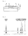
- the polymers 1 to 3 prepared in Preparative Examples 7 to 9 were dissolved in chloroform in a concentration of 1 wt%, respectively. Each solution was applied onto the resulting structure at 1000 rpm to a thickness of 1000 ⁇ , baked under argon atmosphere at 100°C for 1 hour to fabricate OTFT devices shown in Fig. 1.
- An OTFT device was fabricated in the same manner as in Example above, except that polyhexylthiophene commercially available from Aldrich was used as an organic semiconductor material.
- Figs. 7 and 8 shows respectively p-type and n-type current-transfer curves measured from the device using polymer 1.
- Fig. 9 shows a current-transfer curve measured from the device using polyhexylthiophene
- Off-state leakage current was determined by measuring a current flowing at off-state.
- Example Nos. Polymer 1 0.00002 1000 10 -12 Preparative Example 7 Polymer 2 0.0001 1000 10 -11 Preparative Example 8 Polymer 3 0.001 1000 10 -11 Preparative Example 9 Polyhexylthiophene 0.0008 100-400 10 -8 Comparative Example
Landscapes
- Chemical & Material Sciences (AREA)
- Health & Medical Sciences (AREA)
- Chemical Kinetics & Catalysis (AREA)
- Medicinal Chemistry (AREA)
- Polymers & Plastics (AREA)
- Organic Chemistry (AREA)
- Physics & Mathematics (AREA)
- Spectroscopy & Molecular Physics (AREA)
- Engineering & Computer Science (AREA)
- Materials Engineering (AREA)
- Thin Film Transistor (AREA)
- Polyoxymethylene Polymers And Polymers With Carbon-To-Carbon Bonds (AREA)
- Electroluminescent Light Sources (AREA)
- Plural Heterocyclic Compounds (AREA)
- Polymers With Sulfur, Phosphorus Or Metals In The Main Chain (AREA)
Applications Claiming Priority (2)
| Application Number | Priority Date | Filing Date | Title |
|---|---|---|---|
| KR2002084268 | 2002-12-26 | ||
| KR1020020084268A KR100572926B1 (ko) | 2002-12-26 | 2002-12-26 | 폴리티에닐티아졸 유도체 및 이를 이용한 유기박막트랜지스터 |
Publications (2)
| Publication Number | Publication Date |
|---|---|
| EP1434285A2 true EP1434285A2 (de) | 2004-06-30 |
| EP1434285A3 EP1434285A3 (de) | 2005-09-14 |
Family
ID=32464616
Family Applications (1)
| Application Number | Title | Priority Date | Filing Date |
|---|---|---|---|
| EP03257774A Withdrawn EP1434285A3 (de) | 2002-12-26 | 2003-12-10 | Organisches, halbleitendes Polymer und ein organischer Dünnschichttransistor |
Country Status (5)
| Country | Link |
|---|---|
| US (1) | US7019327B2 (de) |
| EP (1) | EP1434285A3 (de) |
| JP (1) | JP4383161B2 (de) |
| KR (1) | KR100572926B1 (de) |
| CN (1) | CN1322030C (de) |
Cited By (4)
| Publication number | Priority date | Publication date | Assignee | Title |
|---|---|---|---|---|
| EP1615237A1 (de) * | 2004-07-08 | 2006-01-11 | Samsung Electronics Co., Ltd | Organische Halbleiter-Polymere enthaltend oligothiophene und n-leitende heteroaromatische Einheiten |
| EP1993105A1 (de) * | 2007-05-16 | 2008-11-19 | Samsung Electronics Co., Ltd. | Organisches Halbleiterpolymer mit Flüssigkristalleigenschaften, organische aktive Schicht, organischer Dünnfilmtransistor und elektronische Vorrichtung damit sowie Herstellungsverfahren dafür |
| EP2083033A1 (de) * | 2008-01-25 | 2009-07-29 | Samsung Electronics Co., Ltd. | Organisches halbleitendes Copolymer und organische Elektrovorrichtung damit |
| US8017795B2 (en) | 2005-04-21 | 2011-09-13 | Ndsu Research Foundation | Radiation curable polymer films having improved laser ablation properties and radiation curable sensitizers therefor |
Families Citing this family (32)
| Publication number | Priority date | Publication date | Assignee | Title |
|---|---|---|---|---|
| WO2000079617A1 (en) * | 1999-06-21 | 2000-12-28 | Cambridge University Technical Services Limited | Aligned polymers for an organic tft |
| CN100483774C (zh) * | 1999-12-21 | 2009-04-29 | 造型逻辑有限公司 | 半导体器件及其形成方法 |
| EP1710266B1 (de) * | 2004-01-26 | 2018-03-07 | Konica Minolta Holdings, Inc. | Organisches halbleitermaterial, organischer transistor, feldeffekttransistor, schaltvorrichtung und thiazolverbindung |
| TWI236173B (en) * | 2004-02-13 | 2005-07-11 | Ind Tech Res Inst | Manufacturing method and device for organic thin film transistor |
| US7057881B2 (en) * | 2004-03-18 | 2006-06-06 | Nanosys, Inc | Nanofiber surface based capacitors |
| US8089152B2 (en) * | 2004-09-16 | 2012-01-03 | Nanosys, Inc. | Continuously variable graded artificial dielectrics using nanostructures |
| US8558311B2 (en) | 2004-09-16 | 2013-10-15 | Nanosys, Inc. | Dielectrics using substantially longitudinally oriented insulated conductive wires |
| US7365395B2 (en) * | 2004-09-16 | 2008-04-29 | Nanosys, Inc. | Artificial dielectrics using nanostructures |
| KR100572854B1 (ko) * | 2004-09-22 | 2006-04-24 | 한국전자통신연구원 | 광반응성 유기고분자 게이트 절연막 조성물 및 이를이용한 유기박막 트랜지스터 |
| KR100669752B1 (ko) * | 2004-11-10 | 2007-01-16 | 삼성에스디아이 주식회사 | 유기 박막 트랜지스터, 이의 제조 방법 및 이를 구비한평판표시장치 |
| KR20060081441A (ko) * | 2005-01-07 | 2006-07-13 | 삼성전자주식회사 | 신규한 티오펜-티아졸 유도체 및 이를 이용한 유기박막트랜지스터 |
| JP4602920B2 (ja) * | 2005-03-19 | 2010-12-22 | 三星モバイルディスプレイ株式會社 | 有機薄膜トランジスタ、それを備えた平板ディスプレイ装置、及び有機薄膜トランジスタの製造方法 |
| KR100647693B1 (ko) * | 2005-05-24 | 2006-11-23 | 삼성에스디아이 주식회사 | 유기박막 트랜지스터 및 그의 제조방법과 유기 박막트랜지스터를 구비한 유기전계 발광표시장치 |
| KR101240656B1 (ko) | 2005-08-01 | 2013-03-08 | 삼성디스플레이 주식회사 | 평판표시장치와 평판표시장치의 제조방법 |
| KR100708720B1 (ko) * | 2005-10-19 | 2007-04-17 | 삼성에스디아이 주식회사 | 유기 박막 트랜지스터, 이의 제조 방법 및 이를 구비한평판 표시 장치 |
| KR100708721B1 (ko) | 2005-10-20 | 2007-04-17 | 삼성에스디아이 주식회사 | 박막 트랜지스터 및 이를 구비한 평판 표시 장치 |
| KR100730159B1 (ko) * | 2005-11-10 | 2007-06-19 | 삼성에스디아이 주식회사 | 유기 박막 트랜지스터, 이를 구비한 평판표시장치, 상기유기 박막 트랜지스터의 제조방법 |
| KR20070053060A (ko) | 2005-11-19 | 2007-05-23 | 삼성전자주식회사 | 표시장치와 이의 제조방법 |
| KR100730180B1 (ko) * | 2005-12-12 | 2007-06-19 | 삼성에스디아이 주식회사 | 유기 박막 트랜지스터 및 이를 구비한 평판 디스플레이장치 |
| US8164087B2 (en) * | 2006-06-12 | 2012-04-24 | Alcatel Lucent | Organic semiconductor compositions with nanoparticles |
| JP5091449B2 (ja) * | 2006-10-03 | 2012-12-05 | 株式会社日立製作所 | 単分子を利用した有機トランジスタ及びfet |
| KR101430260B1 (ko) * | 2007-01-24 | 2014-08-14 | 삼성전자주식회사 | 티아졸 함유 유기반도체 고분자, 이의 제조방법 및 이를이용한 유기박막트랜지스터 |
| KR100824065B1 (ko) * | 2007-02-23 | 2008-05-07 | 재단법인서울대학교산학협력재단 | 광감지용 유기 박막 트랜지스터 |
| JP5152493B2 (ja) * | 2007-03-26 | 2013-02-27 | 国立大学法人大阪大学 | 有機電界効果トランジスター及びその製造方法 |
| JP5135904B2 (ja) * | 2007-06-19 | 2013-02-06 | 株式会社日立製作所 | 有機薄膜トランジスタアレイおよびその製造方法 |
| KR100934534B1 (ko) * | 2007-11-30 | 2009-12-29 | 광주과학기술원 | 티아졸계 유기 반도체 화합물 및 이를 이용한 유기박막트랜지스터 |
| JP2011136921A (ja) * | 2009-12-28 | 2011-07-14 | Jnc Corp | 有機トランジスタ材料およびこれを用いた有機トランジスタ |
| WO2012163464A1 (en) * | 2011-06-01 | 2012-12-06 | Merck Patent Gmbh | Hybrid ambipolar tfts |
| KR101400894B1 (ko) | 2013-05-10 | 2014-05-30 | 한국원자력연구원 | 방사선 기반 높은 일함수를 갖는 그래핀 전극을 이용한 유기 박막 트랜지스터 제조 방법 및 이에 따라 제조되는 유기 박막 트랜지스터 |
| JP6711272B2 (ja) * | 2014-07-23 | 2020-06-17 | 住友化学株式会社 | 高分子化合物およびそれを用いた有機半導体素子 |
| CN110233204B (zh) * | 2019-06-20 | 2023-04-18 | 北京大学深圳研究生院 | 一种有机薄膜晶体管及其制备方法 |
| CN115985917A (zh) * | 2022-12-22 | 2023-04-18 | 广州华星光电半导体显示技术有限公司 | 阵列基板及其制备方法、显示面板 |
Family Cites Families (8)
| Publication number | Priority date | Publication date | Assignee | Title |
|---|---|---|---|---|
| US4505840A (en) * | 1982-07-13 | 1985-03-19 | Chevron Research Company | Heterocyclic electroactive polymers |
| JPH0770708B2 (ja) * | 1986-03-25 | 1995-07-31 | 株式会社東芝 | 電界効果トランジスタ |
| US4892678A (en) * | 1987-02-19 | 1990-01-09 | Agency Of Industrial Science & Technology, Ministry Of International Trade & Industry | Thiophene derivative polymer and a polymer composition thereof |
| US5233017A (en) * | 1992-03-23 | 1993-08-03 | The United States Of America As Represented By The Secretary Of The Air Force | Benzobisthiazole polymers with thiophene moieties |
| US5625199A (en) * | 1996-01-16 | 1997-04-29 | Lucent Technologies Inc. | Article comprising complementary circuit with inorganic n-channel and organic p-channel thin film transistors |
| US6316098B1 (en) * | 1998-03-27 | 2001-11-13 | Yissum Research Development Company Of The Hebrew University Of Jerusalem | Molecular layer epitaxy method and compositions |
| EP1291932A3 (de) * | 2001-09-05 | 2006-10-18 | Konica Corporation | Organisches Dünnfilmhalbleiterelement und dessen Herstellung |
| ATE473251T1 (de) * | 2001-09-29 | 2010-07-15 | Merck Patent Gmbh | Mono-, oligo- und polymere aus benzo(b)thiophen und 2,2'-bisbenzothiophen und ihre verwendung als ladungstransportmaterial |
-
2002
- 2002-12-26 KR KR1020020084268A patent/KR100572926B1/ko not_active Expired - Lifetime
-
2003
- 2003-12-10 EP EP03257774A patent/EP1434285A3/de not_active Withdrawn
- 2003-12-11 US US10/732,243 patent/US7019327B2/en not_active Expired - Lifetime
- 2003-12-26 CN CNB2003101247304A patent/CN1322030C/zh not_active Expired - Fee Related
- 2003-12-26 JP JP2003432203A patent/JP4383161B2/ja not_active Expired - Fee Related
Cited By (10)
| Publication number | Priority date | Publication date | Assignee | Title |
|---|---|---|---|---|
| EP1615237A1 (de) * | 2004-07-08 | 2006-01-11 | Samsung Electronics Co., Ltd | Organische Halbleiter-Polymere enthaltend oligothiophene und n-leitende heteroaromatische Einheiten |
| JP2006037098A (ja) * | 2004-07-08 | 2006-02-09 | Samsung Electronics Co Ltd | ポリ(オリゴチオフェン−アリーレン)誘導体、有機半導体共重合体、半導体多層構造、およびポリ(オリゴチオフェン−アリーレン)誘導体の製造方法 |
| CN1891732B (zh) * | 2004-07-08 | 2011-01-12 | 三星电子株式会社 | 含有低聚噻吩和n-型杂芳族单元的有机半导体共聚物 |
| US8053764B2 (en) | 2004-07-08 | 2011-11-08 | Samsung Electronics Co., Ltd. | Organic semiconductor copolymers containing oligothiophene and η-type heteroaromatic units |
| US8313978B2 (en) | 2004-07-08 | 2012-11-20 | Samsung Electronics Co., Ltd. | Organic semiconductor copolymers containing oligothiophene and n-type heteroaromatic units |
| US8017795B2 (en) | 2005-04-21 | 2011-09-13 | Ndsu Research Foundation | Radiation curable polymer films having improved laser ablation properties and radiation curable sensitizers therefor |
| EP1993105A1 (de) * | 2007-05-16 | 2008-11-19 | Samsung Electronics Co., Ltd. | Organisches Halbleiterpolymer mit Flüssigkristalleigenschaften, organische aktive Schicht, organischer Dünnfilmtransistor und elektronische Vorrichtung damit sowie Herstellungsverfahren dafür |
| US8008426B2 (en) | 2007-05-16 | 2011-08-30 | Samsung Electronics Co., Ltd. | Organic semiconductor polymer having liquid crystal properties, organic active layer, organic thin film transistor, and electronic device including the same, and methods of fabricating the same |
| EP2083033A1 (de) * | 2008-01-25 | 2009-07-29 | Samsung Electronics Co., Ltd. | Organisches halbleitendes Copolymer und organische Elektrovorrichtung damit |
| US7777221B2 (en) | 2008-01-25 | 2010-08-17 | Samsung Electronics Co., Ltd. | Organic semiconducting copolymer and organic electronic device including the same |
Also Published As
| Publication number | Publication date |
|---|---|
| CN1511863A (zh) | 2004-07-14 |
| US20040124410A1 (en) | 2004-07-01 |
| CN1322030C (zh) | 2007-06-20 |
| KR100572926B1 (ko) | 2006-04-24 |
| KR20040057510A (ko) | 2004-07-02 |
| US7019327B2 (en) | 2006-03-28 |
| JP2004211091A (ja) | 2004-07-29 |
| EP1434285A3 (de) | 2005-09-14 |
| JP4383161B2 (ja) | 2009-12-16 |
Similar Documents
| Publication | Publication Date | Title |
|---|---|---|
| EP1434285A2 (de) | Organisches, halbleitendes Polymer und ein organischer Dünnschichttransistor | |
| EP1542294B1 (de) | Organisches Halbleiterpolymer für organische Dünnfilm-Transitoren enthaltend Quionoxalin Ringe im Polymerrückgrat | |
| KR101069519B1 (ko) | 올리고티오펜과 n-형 방향족 화합물을 주쇄에 교호로 포함하는 유기 반도체 고분자 | |
| US8354666B2 (en) | Organic polymer semiconductor, method of preparing the same, and ambipolar organic thin film transistor using the same | |
| US8008426B2 (en) | Organic semiconductor polymer having liquid crystal properties, organic active layer, organic thin film transistor, and electronic device including the same, and methods of fabricating the same | |
| US9184391B2 (en) | Compound having indolocarbazole moiety and divalent linkage | |
| US8058457B2 (en) | Star-shaped oligothiophene-arylene derivatives and organic thin film transistors using the same | |
| EP1672713A1 (de) | Verbindung mit Indolocarbazolresten und dessen Verwendung in elektronischen Vorrichtungen | |
| US20090043113A1 (en) | Heteroacene compound, organic thin film including a heteroacene compound and electronic device including an organic thin film | |
| CA2529245C (en) | Process to form compound with indolocarbazole moieties | |
| EP2270064B1 (de) | Organisches Halbleiterpolymer, Transistor mit einem organischen Halbleiterpolymer und Herstellungsverfahren dafür | |
| KR101450137B1 (ko) | 유기반도체용 공중합체 및 이를 이용한 유기박막트랜지스터 및 유기 전자소자 | |
| EP1605533A2 (de) | Anordnung mit einem kurzkettigen Thiophenoligomer mit divalenter Verknüpfung | |
| KR20130057951A (ko) | 유기 반도체 화합물, 이를 포함하는 유기 박막, 상기 유기 박막을 포함하는 전자 소자 및 유기 박막의 제조방법 | |
| KR101102158B1 (ko) | 신규한 유기 고분자 반도체, 이를 이용한 유기 고분자반도체 박막의 형성방법 및 이를 이용한 유기박막트랜지스터 | |
| KR101430260B1 (ko) | 티아졸 함유 유기반도체 고분자, 이의 제조방법 및 이를이용한 유기박막트랜지스터 | |
| KR101072477B1 (ko) | 고분자 곁사슬에 알킬티오펜 기가 치환된 유기 반도체 화합물 및 이를 이용한 유기 박막 트랜지스터 | |
| US20060151779A1 (en) | Novel thiophene-thiazole derivatives and organic thin film transistors using the same | |
| KR20060108173A (ko) | 신규한 폴리티오펜 유도체 및 이를 이용한 유기박막트랜지스터 |
Legal Events
| Date | Code | Title | Description |
|---|---|---|---|
| PUAI | Public reference made under article 153(3) epc to a published international application that has entered the european phase |
Free format text: ORIGINAL CODE: 0009012 |
|
| AK | Designated contracting states |
Kind code of ref document: A2 Designated state(s): AT BE BG CH CY CZ DE DK EE ES FI FR GB GR HU IE IT LI LU MC NL PT RO SE SI SK TR |
|
| AX | Request for extension of the european patent |
Extension state: AL LT LV MK |
|
| PUAL | Search report despatched |
Free format text: ORIGINAL CODE: 0009013 |
|
| AK | Designated contracting states |
Kind code of ref document: A3 Designated state(s): AT BE BG CH CY CZ DE DK EE ES FI FR GB GR HU IE IT LI LU MC NL PT RO SE SI SK TR |
|
| AX | Request for extension of the european patent |
Extension state: AL LT LV MK |
|
| 17P | Request for examination filed |
Effective date: 20060310 |
|
| AKX | Designation fees paid |
Designated state(s): DE FR GB |
|
| 17Q | First examination report despatched |
Effective date: 20090119 |
|
| STAA | Information on the status of an ep patent application or granted ep patent |
Free format text: STATUS: THE APPLICATION IS DEEMED TO BE WITHDRAWN |
|
| 18D | Application deemed to be withdrawn |
Effective date: 20090530 |