EP2270064B1 - Organisches Halbleiterpolymer, Transistor mit einem organischen Halbleiterpolymer und Herstellungsverfahren dafür - Google Patents
Organisches Halbleiterpolymer, Transistor mit einem organischen Halbleiterpolymer und Herstellungsverfahren dafür Download PDFInfo
- Publication number
- EP2270064B1 EP2270064B1 EP10167763.1A EP10167763A EP2270064B1 EP 2270064 B1 EP2270064 B1 EP 2270064B1 EP 10167763 A EP10167763 A EP 10167763A EP 2270064 B1 EP2270064 B1 EP 2270064B1
- Authority
- EP
- European Patent Office
- Prior art keywords
- chemical formula
- organic semiconductor
- semiconductor polymer
- same
- perfluoroalkyl
- Prior art date
- Legal status (The legal status is an assumption and is not a legal conclusion. Google has not performed a legal analysis and makes no representation as to the accuracy of the status listed.)
- Active
Links
- 0 CCCCCCCCC1(C)c2cc(C3=CCC(C4SC(C(C)(CC)c(cc5F)cc(F)c5F)=CC4)S3)ccc2-c2c1cc(C(*)(CC)c(cc1F)cc(F)c1F)cc2 Chemical compound CCCCCCCCC1(C)c2cc(C3=CCC(C4SC(C(C)(CC)c(cc5F)cc(F)c5F)=CC4)S3)ccc2-c2c1cc(C(*)(CC)c(cc1F)cc(F)c1F)cc2 0.000 description 15
Images





Classifications
-
- C—CHEMISTRY; METALLURGY
- C08—ORGANIC MACROMOLECULAR COMPOUNDS; THEIR PREPARATION OR CHEMICAL WORKING-UP; COMPOSITIONS BASED THEREON
- C08G—MACROMOLECULAR COMPOUNDS OBTAINED OTHERWISE THAN BY REACTIONS ONLY INVOLVING UNSATURATED CARBON-TO-CARBON BONDS
- C08G61/00—Macromolecular compounds obtained by reactions forming a carbon-to-carbon link in the main chain of the macromolecule
- C08G61/12—Macromolecular compounds containing atoms other than carbon in the main chain of the macromolecule
- C08G61/122—Macromolecular compounds containing atoms other than carbon in the main chain of the macromolecule derived from five- or six-membered heterocyclic compounds, other than imides
- C08G61/123—Macromolecular compounds containing atoms other than carbon in the main chain of the macromolecule derived from five- or six-membered heterocyclic compounds, other than imides derived from five-membered heterocyclic compounds
- C08G61/126—Macromolecular compounds containing atoms other than carbon in the main chain of the macromolecule derived from five- or six-membered heterocyclic compounds, other than imides derived from five-membered heterocyclic compounds with a five-membered ring containing one sulfur atom in the ring
-
- H—ELECTRICITY
- H10—SEMICONDUCTOR DEVICES; ELECTRIC SOLID-STATE DEVICES NOT OTHERWISE PROVIDED FOR
- H10K—ORGANIC ELECTRIC SOLID-STATE DEVICES
- H10K10/00—Organic devices specially adapted for rectifying, amplifying, oscillating or switching; Organic capacitors or resistors having potential barriers
- H10K10/40—Organic transistors
- H10K10/46—Field-effect transistors, e.g. organic thin-film transistors [OTFT]
- H10K10/462—Insulated gate field-effect transistors [IGFETs]
- H10K10/464—Lateral top-gate IGFETs comprising only a single gate
-
- H—ELECTRICITY
- H10—SEMICONDUCTOR DEVICES; ELECTRIC SOLID-STATE DEVICES NOT OTHERWISE PROVIDED FOR
- H10K—ORGANIC ELECTRIC SOLID-STATE DEVICES
- H10K10/00—Organic devices specially adapted for rectifying, amplifying, oscillating or switching; Organic capacitors or resistors having potential barriers
- H10K10/40—Organic transistors
- H10K10/46—Field-effect transistors, e.g. organic thin-film transistors [OTFT]
- H10K10/462—Insulated gate field-effect transistors [IGFETs]
- H10K10/466—Lateral bottom-gate IGFETs comprising only a single gate
-
- H—ELECTRICITY
- H10—SEMICONDUCTOR DEVICES; ELECTRIC SOLID-STATE DEVICES NOT OTHERWISE PROVIDED FOR
- H10K—ORGANIC ELECTRIC SOLID-STATE DEVICES
- H10K10/00—Organic devices specially adapted for rectifying, amplifying, oscillating or switching; Organic capacitors or resistors having potential barriers
- H10K10/40—Organic transistors
- H10K10/46—Field-effect transistors, e.g. organic thin-film transistors [OTFT]
- H10K10/462—Insulated gate field-effect transistors [IGFETs]
- H10K10/484—Insulated gate field-effect transistors [IGFETs] characterised by the channel regions
-
- H—ELECTRICITY
- H10—SEMICONDUCTOR DEVICES; ELECTRIC SOLID-STATE DEVICES NOT OTHERWISE PROVIDED FOR
- H10K—ORGANIC ELECTRIC SOLID-STATE DEVICES
- H10K85/00—Organic materials used in the body or electrodes of devices covered by this subclass
- H10K85/10—Organic polymers or oligomers
- H10K85/111—Organic polymers or oligomers comprising aromatic, heteroaromatic, or aryl chains, e.g. polyaniline, polyphenylene or polyphenylene vinylene
- H10K85/113—Heteroaromatic compounds comprising sulfur or selene, e.g. polythiophene
-
- H—ELECTRICITY
- H10—SEMICONDUCTOR DEVICES; ELECTRIC SOLID-STATE DEVICES NOT OTHERWISE PROVIDED FOR
- H10K—ORGANIC ELECTRIC SOLID-STATE DEVICES
- H10K85/00—Organic materials used in the body or electrodes of devices covered by this subclass
- H10K85/10—Organic polymers or oligomers
- H10K85/111—Organic polymers or oligomers comprising aromatic, heteroaromatic, or aryl chains, e.g. polyaniline, polyphenylene or polyphenylene vinylene
- H10K85/115—Polyfluorene; Derivatives thereof
-
- H—ELECTRICITY
- H10—SEMICONDUCTOR DEVICES; ELECTRIC SOLID-STATE DEVICES NOT OTHERWISE PROVIDED FOR
- H10K—ORGANIC ELECTRIC SOLID-STATE DEVICES
- H10K85/00—Organic materials used in the body or electrodes of devices covered by this subclass
- H10K85/10—Organic polymers or oligomers
- H10K85/151—Copolymers
-
- C—CHEMISTRY; METALLURGY
- C08—ORGANIC MACROMOLECULAR COMPOUNDS; THEIR PREPARATION OR CHEMICAL WORKING-UP; COMPOSITIONS BASED THEREON
- C08G—MACROMOLECULAR COMPOUNDS OBTAINED OTHERWISE THAN BY REACTIONS ONLY INVOLVING UNSATURATED CARBON-TO-CARBON BONDS
- C08G2261/00—Macromolecular compounds obtained by reactions forming a carbon-to-carbon link in the main chain of the macromolecule
- C08G2261/10—Definition of the polymer structure
- C08G2261/14—Side-groups
- C08G2261/146—Side-chains containing halogens
-
- C—CHEMISTRY; METALLURGY
- C08—ORGANIC MACROMOLECULAR COMPOUNDS; THEIR PREPARATION OR CHEMICAL WORKING-UP; COMPOSITIONS BASED THEREON
- C08G—MACROMOLECULAR COMPOUNDS OBTAINED OTHERWISE THAN BY REACTIONS ONLY INVOLVING UNSATURATED CARBON-TO-CARBON BONDS
- C08G2261/00—Macromolecular compounds obtained by reactions forming a carbon-to-carbon link in the main chain of the macromolecule
- C08G2261/10—Definition of the polymer structure
- C08G2261/16—End groups
- C08G2261/164—End groups comprising organic end groups
- C08G2261/1644—End groups comprising organic end groups comprising other functional groups, e.g. OH groups, NH groups, COOH groups or boronic acid
-
- C—CHEMISTRY; METALLURGY
- C08—ORGANIC MACROMOLECULAR COMPOUNDS; THEIR PREPARATION OR CHEMICAL WORKING-UP; COMPOSITIONS BASED THEREON
- C08G—MACROMOLECULAR COMPOUNDS OBTAINED OTHERWISE THAN BY REACTIONS ONLY INVOLVING UNSATURATED CARBON-TO-CARBON BONDS
- C08G2261/00—Macromolecular compounds obtained by reactions forming a carbon-to-carbon link in the main chain of the macromolecule
- C08G2261/10—Definition of the polymer structure
- C08G2261/18—Definition of the polymer structure conjugated
-
- C—CHEMISTRY; METALLURGY
- C08—ORGANIC MACROMOLECULAR COMPOUNDS; THEIR PREPARATION OR CHEMICAL WORKING-UP; COMPOSITIONS BASED THEREON
- C08G—MACROMOLECULAR COMPOUNDS OBTAINED OTHERWISE THAN BY REACTIONS ONLY INVOLVING UNSATURATED CARBON-TO-CARBON BONDS
- C08G2261/00—Macromolecular compounds obtained by reactions forming a carbon-to-carbon link in the main chain of the macromolecule
- C08G2261/40—Polymerisation processes
- C08G2261/41—Organometallic coupling reactions
- C08G2261/411—Suzuki reactions
-
- C—CHEMISTRY; METALLURGY
- C08—ORGANIC MACROMOLECULAR COMPOUNDS; THEIR PREPARATION OR CHEMICAL WORKING-UP; COMPOSITIONS BASED THEREON
- C08G—MACROMOLECULAR COMPOUNDS OBTAINED OTHERWISE THAN BY REACTIONS ONLY INVOLVING UNSATURATED CARBON-TO-CARBON BONDS
- C08G2261/00—Macromolecular compounds obtained by reactions forming a carbon-to-carbon link in the main chain of the macromolecule
- C08G2261/40—Polymerisation processes
- C08G2261/41—Organometallic coupling reactions
- C08G2261/414—Stille reactions
-
- C—CHEMISTRY; METALLURGY
- C08—ORGANIC MACROMOLECULAR COMPOUNDS; THEIR PREPARATION OR CHEMICAL WORKING-UP; COMPOSITIONS BASED THEREON
- C08G—MACROMOLECULAR COMPOUNDS OBTAINED OTHERWISE THAN BY REACTIONS ONLY INVOLVING UNSATURATED CARBON-TO-CARBON BONDS
- C08G2261/00—Macromolecular compounds obtained by reactions forming a carbon-to-carbon link in the main chain of the macromolecule
- C08G2261/90—Applications
- C08G2261/92—TFT applications
-
- Y—GENERAL TAGGING OF NEW TECHNOLOGICAL DEVELOPMENTS; GENERAL TAGGING OF CROSS-SECTIONAL TECHNOLOGIES SPANNING OVER SEVERAL SECTIONS OF THE IPC; TECHNICAL SUBJECTS COVERED BY FORMER USPC CROSS-REFERENCE ART COLLECTIONS [XRACs] AND DIGESTS
- Y02—TECHNOLOGIES OR APPLICATIONS FOR MITIGATION OR ADAPTATION AGAINST CLIMATE CHANGE
- Y02E—REDUCTION OF GREENHOUSE GAS [GHG] EMISSIONS, RELATED TO ENERGY GENERATION, TRANSMISSION OR DISTRIBUTION
- Y02E10/00—Energy generation through renewable energy sources
- Y02E10/50—Photovoltaic [PV] energy
- Y02E10/549—Organic PV cells
Definitions
- Example embodiments relate to an organic semiconductor polymer, a transistor including an organic semiconductor polymer and methods of fabricating the same.
- CTR cathode ray tube
- LCD liquid crystal display
- OLED organic light emitting diode
- PDP plasma display panel
- SED surface-conduction electron-emitter display
- a thin film transistor (TFT) including a semiconductor layer of amorphous silicon is generally used for a switching device in flat panel displays.
- the amorphous silicon thin film transistor is used because good uniformity and high electrical characteristics are observed in a doping state, and good insulating characteristics are observed in a non-doping state.
- the organic thin film transistor generally includes a substrate, a gate electrode, an insulation layer, a source electrode, a drain electrode and a channel region.
- the transistor may be classified as a bottom contact (BC) type in which a channel region is formed on the source electrode and the drain electrode (and after formation of a metal electrode), or a top contact (TC) type of which a metal electrode is formed on, and after, the channel region due to mask deposition.
- BC bottom contact
- TC top contact
- the low molecular, or oligomer, organic semiconductor material filled in the channel region of the organic thin film transistor may include merocyanine, phthalocyanine, perylene, pentacene, C60, a thiophene oligomer and/or similar compounds.
- the low molecular, or oligomer, organic semiconductor material may be a thin film formed on the channel region according to a vacuum process.
- EP 0 414 906 A1 discloses a fluoroalkylated heteroaromatic polymer having a degree of polymerization of 5-5,000 and comprising repeating units of the following general formula: wherein R stands for a hydrogen atom or an alkyl group bearing 1-25 carbon atoms, X stands for a sulfur atom, imino group or an oxygen atom and n is an integer of 1-9.
- a polymeric material comprises at least one repeat unit consisting substantially of a moiety of Formula: in which Y 1 represents N, P, S, As and/or Se.
- Ar 1 and Ar 2 which may the same or different, represent independently a multivalent, optionally substituted aromatic group and Ar 3 represents independently a mono or multivalent, optionally substituted aromatic group.
- EP 2 006 291 A1 discloses a fused ring compound represented by the following general formula: wherein R 11 and R 12 each independently represent a hydrogen atom, an alkyl group having 1 to 20 carbon atoms, an alkoxy group, an alkylthio group, an alkylamino group, an alkoxycarbonyl group, an optionally substituted aryl group having 6 to 60 carbon atoms, an optionally substituted heterocyclic group having 4 to 60 carbon atoms, or a cyano group, provided that at least one of R 11 and R 12 is not a hydrogen atom; R 13 and R 14 each independently represent a monovalent group, and n and m each independently denote an integer of 0 to 2; and Y 11 and Y 12 are each independently a divalent group comprising a sulfur atom, an oxygen atom, a nitrogen atom, a selenium atom or a tellurium atom.
- WO 2008/111461 A1 discloses a fluorine-containing polymer of general formula: wherein Ar 1 and Ar 2 each independently represent an aromatic hydrocarbon group having at least six carbon atoms or a heterocyclic group having at least four carbon atoms; R 1 , R 2 , R 3 and R 4 each independently represent a hydrogen atom, a halogen atom, or a monovalent group; R 5 and R 6 each independently represent a hydrogen atom or a monovalent organic group that may be substituted with a substituent; s 1 and t 1 each independently represent an integer of at least 2; with the proviso that at least one of R 5 and R 6 is the abovementioned monovalent organic group where at least one of all the hydrogen atoms of the monovalent organic group including the substituent is substituted with a fluorine atom.
- Newman C et al. "Introduction to organic Thin Film Transistors and Design of n-Channel Organic Semiconductors", Chemistry of Materials, American Chemical Society, Vol. 16, no. 23, 4436-4451 discloses a the development of new n-channel materials.
- Li L et al. "Turning the Electronic Structure of Conjugated Polymers with Fluoroalkyl Substitution: Alternating Alkyl/Perfluoroalkyl-Substituted Polythiophene", Macromolecules, American Chemical Society, 2005, 38, 372-378 discloses polythiophenes modified by the inclusion of alkyl and perfluoroalkyl substituents. Facchetti et al.
- n-Type Building Blocks for Organic Electronics A Homologous Family of Fluorocarbon-Substituted Thiophene Oligomers with High Carrier Mobility
- Advanced Materials 2003, 15, no. 1, 33-39 discloses an n-type thiophene-based conductor.
- WO 02/09201 discloses n-type thiophene semiconductors.
- WO 03/010778 discloses n-type thiophene semiconductors.
- Example embodiments relate to an organic semiconductor polymer, a transistor including an organic semiconductor polymer and methods of fabricating the same.
- Example embodiments provide an organic semiconductor polymer, which imparts increased charge mobility, electrical stability and/or air stability, and a method of fabricating the same using a solution-based process.
- Example embodiments provide a transistor including an organic semiconductor polymer, which has increased charge mobility, electrical stability and/or air stability, and a method of fabricating the same using a solution-based process.
- an electronic device including an organic semiconductor polymer, and a method of fabricating the same using a solution-based process.
- an organic semiconductor polymer represented by Chemical Formula (1), shown below, is provided.
- R 3 to R 9 are the same or different and are independently selected from the group consisting of the fluoro, the C1 to C20 partially fluorinated alkyl, the C1 to C20 perfluoroalkyl (C n F 2n+1 ) and combinations thereof.
- R 1 and R 2 are the same, or different, and are independently selected from the group consisting of hydrogen, a fluoro, a C1 to C30 linear or branched alkyl, a C3 to C30 cycloalkyl, a C1 to C20 partially fluorinated alkyl, a C1 to C20 perfluoroalkyl (C n F 2n+1 ), a C1 to C30 linear or branched alkoxy, a C3 to C30 cycloalkoxy, a C2 to C30 linear or branched alkoxyalkyl, a C4 to C30 cycloalkoxyalkyl, and combinations thereof.
- R 1 and R 2 may be the same or different and may be independently selected from the group consisting of the fluoro, the C1 to C20 partially fluorinated alkyl, the C1 to C20 perfluoroalkyl (C n F 2n+1 ) and combinations thereof.
- n is a polymerization degree and an integer of 8 or more.
- the organic semiconductor polymer may be a p-type organic semiconductor polymer.
- Ar is represented by one of the following Chemical Formula (2), (5) and (6) shown below.
- R 1 1 is hydrogen or a C1 to C20 alkyl
- Ar 1 is selected from the group consisting of Chemical Formulae (3-1) to (3-27), thiadiazole, oxadiazole, pyrazole, triazole, tetrazole, pyridazine, isoquinoline, napthyridine, pyrimidopyrimidine, pyridopyrimidine, benzothiazole, benzooxazole, phenanthridine
- Y is hydrogen, a C1 to C20 linear or branched alkyl, a C3 to C20 cycloalkyl, a C6 to C30 aryl, a C1 to C16 linear or branched alkoxy, or a C3 to C16
- x is an integer ranging from 1 to 12
- y is an integer ranging from 1 to 4
- X b and X c are the same or different and are independently N
- Y 1 and Y 2 are the same or different and are independently S or Se
- R 14 to R 19 are the same or different and are independently hydrogen or a C1 to C20 alkyl
- m is 0 to 2.
- R 20 , R' 20 , R 21 , and R ' 21 are the same or different and are independently hydrogen or a C1 to C20 alkyl.
- Chemical Formula (5) for example, may be represented by Chemical Formula (5-1) shown below.
- R' 14 to R ' 19 are the same or different and are independently hydrogen or a C1 to C20 alkyl.
- Chemical Formula (6) for example, may be represented by Chemical Formula (6-1), shown below.
- R 2 0 and R ' 20 are the same or different and are independently hydrogen or a C1 to C20 alkyl.
- the organic semiconductor polymer may include a terminal functional group represented by Chemical Formulae (7) to (10), shown below.
- R is a fluoro or a C1 to C20 perfluoroalkyl, and a is an integer ranging from 1 to 5.
- R is a fluoro or a C1 to C20 perfluoroalkyl and a is an integer ranging from 1 to 6.
- R is a fluoro or a C1 to C20 perfluoroalkyl, and a is an integer ranging from 1 to 3.
- R is a fluoro or a C1 to C20 perfluoroalkyl and a is an integer ranging from 1 to 3.
- a transistor including the organic semiconductor polymer is provided.
- the transistor includes a gate electrode positioned on a substrate, a source electrode and a drain electrode facing each other and defining a channel region, an insulation layer that electrically insulates the source electrode, the drain electrode and the gate electrode, and an active layer including the organic semiconductor polymer in the channel region.
- an electronic device including the organic semiconductor polymer may be a memory device, an organic light emitting diode (OLED), an electronic paper (e-paper), a radio-frequency identification (RFID) tag, a flat-panel display including an active-matrix flat-panel display (AMFPD), a sensor including a photosensor, a biosensor, a chemical sensor or combinations thereof (e.g., a biochemical sensor, photochemical sensor, etc.), a laser device, a photovoltaic device (e.g., a solar cell) or similar devices.
- OLED organic light emitting diode
- e-paper electronic paper
- RFID radio-frequency identification
- AMFPD active-matrix flat-panel display
- a sensor including a photosensor, a biosensor, a chemical sensor or combinations thereof e.g., a biochemical sensor, photochemical sensor, etc.
- a laser device e.g., a photovoltaic device or similar devices.
- Yet other example embodiments relate to a method of synthesizing an organic semiconductor polymer including forming the organic semiconductor polymer having Chemical Formula (1) by reacting monomer (1A) with compound (1B) to as shown in Reaction Scheme (1), as shown below.
- X 1 , X 2 , Y 1 , and Y 2 are independently reactive groups selected from the group consisting of a halogen group, a trialkyl tin group and a borane group.
- R 3 to R 9 may be the same, or different, and may be independently selected from the group consisting of the fluoro, the C1 to C20 partially fluorinated alkyl, the C1 to C20 perfluoroalkyl (C n F 2n+1 ) and combinations thereof.
- R 1 and R 2 may be the same, or different, and may be independently selected from the group consisting of hydrogen, a fluoro, a C1 to C30 linear or branched alkyl, a C3 to C30 cycloalkyl, a C1 to C20 partially fluorinated alkyl, a C1 to C20 perfluoroalkyl (C n F 2n+1 ), a C1 to C30 linear or branched alkoxy, a C3 to C30 cycloalkoxy, a C2 to C30 linear or branched alkoxyalkyl, a C4 to C30 cycloalkoxyalkyl and combinations thereof.
- R 1 and R 2 may be the same, or different, and may be independently selected from the group consisting of the fluoro, the C1 to C20 partially fluorinated alkyl, the C1 to C20 perfluoroalkyl (C n F 2n+1 ) and combinations thereof.
- Ar and Ar' are independently a substituted or unsubstituted C6 to C30 aromatic ring, a substituted or unsubstituted C2 to C14 heteroaromatic ring, or a substituted or unsubstituted C6 to C30 condensed polycycle.
- n is a polymerization degree and an integer of 8 or more.
- Compound (1B) may be used in an amount of about 5 to about 10 equivalents with respect to the monomer (1A).
- the trialkyl tin partially fluorinated may be represented by Chemical Formula (38), shown below.
- R31 to R33 are the same or different and are independently hydrogen or a C1 to C7 alkyl, provided that at least one of R31 to R33 is an alkyl.
- the borane group may be represented by one of Chemical Formula (39) or Chemical Formula (40), as shown below.
- R 34 to R 37 are the same or different and are independently hydrogen or a C1 to C7 alkyl, provided that at least one of R 34 to R 37 is an alkyl.
- the method may include performing the reaction of monomer (1A) with compound (1B) in the presence of a catalyst.
- the catalyst may be an organic metal catalyst represented by one of Chemical Formulae (41-1) to (41-4), as shown below. Pd(L 1 ) x CHEMICAL FORMULA (41-1) Pd(L 2 ) 4-y Cl y CHEMICAL FORMULA (41-2)
- L 1 and L 2 are ligands selected from the group consisting of triphenylphosphine (PPh 3 ), 1,4-bis(diphenylphosphine)butane (dppb), 1,1'-bis(diphenylphosphino)ferrocene (dppf), acetate (OAc), triphenyl arsine (AsPh 3 ) and triphenylphosphite (P(OPh) 3 ), x is an integer ranging from 2 to 4, and y is an integer ranging from 1 to 3.
- L 3 and L 4 are ligands selected from the group consisting of a bis(diphenylphosphino)alkane and a cycloalkene, and x is an integer of 2 or 3, and y is an integer of 1 or 2.
- the bis(diphenylphosphino) alkane may be selected from the group consisting of 1,3-bis(diphenylphosphino)propane (dppp), 1,2-bis(diphenylphosphino)ethane (dppe), 1,4-bis(diphenylphosphino)butane (dppb) and combinations thereof.
- the cycloalkene may be 1,5-cyclooctadiene (COD).
- FIGS. 1-10 represent non-limiting, example embodiments as described herein.
- spatially relative terms e.g., "beneath,” “below,” “lower,” “above,” “upper” and the like
- the spatially relative terms are intended to encompass different orientations of the device in use or operation in addition to the orientation depicted in the figures. For example, if the device in the figures is turned over, elements described as “below” or “beneath” other elements or features would then be oriented “above” the other elements or features.
- the term “below” can encompass both an orientation that is above, as well as, below.
- the device may be otherwise oriented (rotated 90 degrees or viewed or referenced at other orientations) and the spatially relative descriptors used herein should be interpreted accordingly.
- Example embodiments are described herein with reference to cross-sectional illustrations that are schematic illustrations of idealized embodiments (and intermediate structures). As such, variations from the shapes of the illustrations as a result, for example, of manufacturing techniques and/or tolerances, may be expected. Thus, example embodiments should not be construed as limited to the particular shapes of regions illustrated herein but may include deviations in shapes that result, for example, from manufacturing. For example, an implanted region illustrated as a rectangle may have rounded or curved features and/or a gradient ( e.g., of implant concentration) at its edges rather than an abrupt change from an implanted region to a non-implanted region.
- a gradient e.g., of implant concentration
- a buried region formed by implantation may result in some implantation in the region between the buried region and the surface through which the implantation may take place.
- the regions illustrated in the figures are schematic in nature and their shapes do not necessarily illustrate the actual shape of a region of a device and do not limit the scope.
- aromatic group or “aromatic ring” refers to a functional group including a C4 to C30 aromatic cyclic group
- heteroaryl or “heteroaromatic ring” refers to a C2 to C30 heteroaryl or a C3 to C30 heterocycloalkenyl
- condensed polycycle refers to a fused ring of at least two cyclic groups selected from the group consisting of the above-described aromatic group and heteroaromatic group, a C3 to C30 cycloalkyl, and a C3 to C30 cycloalkenyl.
- heteroaryl refers to a C2 to C30 heteroaryl or heteroarylene
- aryl refers to a C6 to C30 aryl or arylene
- alkyl refers to a C1 to C30 alkyl
- hetero refers to one including heteroatoms selected from the group consisting of N, O, S, Si, and P, and including 1 to 4 heteroatoms in one ring.
- substituted refers to one substituted with at least a functional group selected from the group consisting of a fluoro, a C1 to C30 linear or branched alkyl, a C3 to C30 cycloalkyl, a C1 to C20 partially fluorinated alkyl, a C1 to C20 perfluoroalkyl (C n F 2n+1 ), a C1 to C30 linear or branched alkoxy, a C3 to C30 cycloalkoxy, a C2 to C30 linear or branched alkoxyalkyl, a C4 to C30 cycloalkoxyalkyl and combinations thereof in a functional group or a compound.
- a functional group selected from the group consisting of a fluoro, a C1 to C30 linear or branched alkyl, a C3 to C30 cycloalkyl, a C1 to C20 partially fluorinated alkyl, a C1 to C20 perfluoroalky
- Example embodiments relate to an organic semiconductor polymer, a transistor including an organic semiconductor polymer and methods of fabricating the same.
- an organic semiconductor polymer represented by Chemical Formula (1), shown below, is provided.
- R 1 and R 2 are the same or different and are independently selected from the group consisting of hydrogen, a fluoro, a C1 to C30 linear or branched alkyl, a C3 to C30 cycloalkyl, a C1 to C20 partially fluorinated alkyl, a C1 to C20 perfluoroalkyl (C n F 2n+1 ), a C1 to C30 linear or branched alkoxy, a C3 to C30 cycloalkoxy, a C2 to C30 linear or branched alkoxyalkyl, a C4 to C30 cycloalkoxyalkyl and combinations thereof.
- n refers to a polymerization degree, and is an integer of 8 or more.
- R 1 and R 2 are present in plural and a plurality of R 1 and R 2 are the same or different from each other.
- n refers to a polymerization degree and may be an integer of 8 or more, or an integer of 8 to 200.
- the organic semiconductor polymer may have a number average molecular weight (Mn) of about 5,000 to about 200,000 and/or about 10,000 to about 50,000 ( e.g., about 5,000 to about 50,000 or about 10,000 to about 200,000).
- the organic semiconductor polymer may be a p -type organic semiconductor polymer.
- Ar is represented by one of the following Chemical Formula (2), (5) and (6) shown below.
- R 11 is hydrogen or a C1 to C20 alkyl
- Ar 1 is selected from the group consisting of functional groups represented by Chemical Formulae (3-1) to (3-27), thiadiazole, oxadiazole, pyrazole, triazole, tetrazole, pyridazine, isoquinoline, naphthyridine, pyrimidopyrimidine, pyridopyrimidine, benzothiazole, benzooxazole, phenanthridine
- Y is hydrogen, a C1 to C20 linear or branched alkyl, a C3 to C20 cycloalkyl, a C6 to C30 aryl, a C1 to C16 linear or branched alkoxy, or a C3 to C16 cycloalkoxyalkyl.
- X b and X c are N
- Y 1 and Y 2 are the same or different and are independently S or Se
- R 14 to R 19 are the same or different and are independently hydrogen or a C1 to C20 alkyl ( e . g ., C 6 H 13 , C 8 H 17 , C 10 H 21 , C 12 H 25 , C 14 H 29 or C 16 H 33 )
- m is 0 or 1.
- the R 14 , R 17 , R 18 , and R 19 groups may be present, respectively, in a five-membered ring in twos (e.g., two R 14 groups may be present in a five-membered ring, and/or two R 18 groups may be present in another five-membered ring), and the two respective groups in each ring may be the same or different from each other.
- R 20 , R' 20 , R 21 , and R ' 21 are the same or different, and are independently hydrogen or a C1 to C20 alkyl ( e.g., C 6 H 13 , C 8 H 17 , C 10 H 21 , C 12 H 25 , C 14 H 29 , or C 16 H 33 ).
- the R 2 0 and R ' 20 groups may be present, respectively, in a five-membered ring in twos, and the two respective groups in each ring may be the same or different from each other.
- Chemical Formula (5) for example, may be Chemical Formula (5-1) shown below.
- R' 14 to R' 19 are the same or different, and are independently hydrogen or a C1 to C20 alkyl ( e.g ., C 6 H 13 , C 8 H 17 , C 10 H 21 , C 12 H 25 , C 14 H 29 or C 16 H 33 ).
- the R' 14 , R' 17 , R' 18 , and R' 19 groups may be present, respectively, in a five-membered ring in twos, and the two respective groups in each ring may be the same or different from each other.
- Chemical Formula (6) for example, may be Chemical Formula (6-1), shown below.
- R 20 and R ' 20 are the same or different, and are independently hydrogen or a C1 to C20 alkyl ( e.g ., C 6 H 13 , C 8 H 17 , C 10 H 21 , C 12 H 25 , C 14 H 29 or C 16 H 33 ).
- the R ' 20 and R ' 20 groups may be present, respectively, in a five-membered ring in twos, and the two respective groups in each ring may be the same or different from each other.
- the organic semiconductor polymer may include a terminal functional group represented by Chemical Formulae (7) to (10), shown below.
- R is a fluoro or a C1 to C20 perfluoroalkyl, and a is an integer ranging from 1 to 5, or an integer ranging from 1 to 4.
- R is a fluoro or a C1 to C20 perfluoroalkyl
- a is an integer ranging from 1 to 6, or an integer ranging from 1 to 5.
- R is a fluoro or a C1 to C20 perfluoroalkyl, and a is an integer ranging from 1 to 3 or 1 to 2.
- R is a fluoro or a C1 to C20 perfluoroalkyl, and a is an integer ranging from 1 to 3, or an integer from 1 to 2.
- the organic semiconductor polymer of the invention may include the compounds represented by Chemical Formulae (11) to (37), shown below.
- Chemical Formulae (11) to (37) n is the same as in the above Chemical Formula (1).
- the organic semiconductor polymer represented by Chemical Formula (1) may be synthesized according to methods disclosed in Stille et al. (Angew. Chem. Int. Ed. Engl. 1986, Vol. 25, pp. 508-524 ), Suzuki et al. (J. Am. Chem. Soc. 1989, Vol. 111, pp. 314-321 ), McCullough et al. (US 6,166,172, 1999 ), or Yamamoto et al. (Macromolecules 1992, Vol. 25, pp. 1214-1226 ). As shown in Reaction Scheme (1), the organic semiconductor polymer may be synthesized by reacting monomer (1A) (which functions as a polymer main chain) with compound (1B) (which functions as a terminal functional group).
- the compound (1B), constituting a terminal functional group is used in an amount of about 5 to about 10 equivalents with respect to the monomer (1A).
- Ar' is the same as Ar in Chemical Formula (1)
- X 1 , X 2 , Y 1 , and Y 2 are independently reactive groups selected from the group consisting of a halogen (e.g ., Br, I, Cl and other halogen elements) group, a trialkyl tin group and a borane group.
- a halogen e.g ., Br, I, Cl and other halogen elements
- G 1 , G 2 , R 1 , R 2 , Ar , n, a, and b are the same as defined in the above Chemical Formula (1).
- the trialkyl tin group may be represented by Chemical Formula (38), shown below, and the borane compound may be represented by Chemical Formula (39) or Chemical Formula (40), both shown below.
- R 31 to R 33 are the same or different, and are independently hydrogen or a C1 to C7 alkyl, provided that at least one of R 31 to R 33 is an alkyl.
- R 34 to R 37 are the same or different, and are independently hydrogen or a C1 to C7 alkyl, provided that at least one of R 34 to R 37 is an alkyl.
- a catalyst may be used in the reaction of the Reaction Scheme (1), and may be an organic metal catalyst represented by Chemical Formulae (41-1) to (41-4), all of which are shown below.
- Chemical Formulae (41-1) to (41-4) Pd(L 1 ) x CHEMICAL FORMULA (41-1)
- L 1 and L 2 are ligands selected from the group consisting of triphenylphosphine (PPh 3 ), 1,4-bis(diphenylphosphine)butane (dppb), 1,1'-bis(diphenylphosphino)ferrocene (dppf), acetate (OAc), triphenyl arsine (AsPh 3 ) and triphenylphosphite (P(OPh) 3 ), x is an integer ranging from 2 to 4, and y is an integer ranging from 1 to 3.
- L 3 and L 4 are ligands selected from the group consisting of a bis(diphenylphosphino)alkane (e.g., 1,3-bis(diphenylphosphino)propane (dppp), 1,2-bis(diphenylphosphino)ethane (dppe), 1,4-bis(diphenylphosphino) butane (dppb) and the like) and a cycloalkene (e.g ., 1,5-cyclooctadiene (COD) and the like), x is an integer of 2 or 3, and y is an integer of 1 or 2.
- a bis(diphenylphosphino)alkane e.g., 1,3-bis(diphenylphosphino)propane (dppp), 1,2-bis(diphenylphosphino)ethane (dppe), 1,4-bis(diphenylphosphino) butane (dppb) and the like
- palladium catalysts examples include a palladium (0) catalyst (e.g., a tetrakis(triphenylphosphine)palladium (0) compound (Pd(PPh 3 ) 4 )) and palladium (II) catalysts ( e.g., bis(triphenylphosphine)palladium(II) dichloride (PdCl 2 (PPh 3 ) 2 ), [1,4-bis(diphenylphosphine)butane]palladium (II) dichloride (Pd(dppb)Cl 2 ), [1,1'-bis(diphenylphosphino)ferrocene]palladium (II) dichloride (Pd(dppf)Cl 2 ), palladium (II) acetate (Pd(OAc) 2 ) and the like).
- a palladium (0) catalyst e.g., a tetrakis(triphenylphosphine
- nickel catalysts examples include a nickel (0) catalyst (e.g., a bis(1,5-cyclooctadiene) nickel (0) compound (Ni(COD) 2 )) and a nickel (II) catalyst (e.g., 1,3-diphenylphosphinopropane nickel (II) chloride (Ni(dppp)Cl 2 ), 1,2-bis(diphenylphosphino)ethane nickel (II) chloride (Ni(dppe)Cl 2 ) and the like).
- the catalyst may be used by adjusting its amount according to amounts of the monomers.
- the tetrakis(triphenyl phosphine) palladium (0) compound may be used at about 0.2-mol% to about 15-mol% with respect to monomers or at about 2-mol% to about 10-mol% with respect to monomers.
- the tetrakis(triphenyl phosphine) palladium (0) compound may be used at about 0.2-mol% to about 10-mol% with respect to monomers, or at about 2-mol% to about 15-mol% with respect to monomers.
- a polymerization solvent e.g., toluene, dimethylformamide (DMF), tetrahydrofuran (THF), N-methylpyrrolidone (NMP) and the like
- Condensation reaction may be performed at about 80°C to about 120°C for about 6-hours to about 48-hours under a nitrogen atmosphere.
- the organic semiconductor polymer may be applied to an active layer of a transistor.
- the transistor may include a gate electrode positioned on a substrate, a source electrode and a drain electrode facing each other and defining a channel region, an insulation layer that electrically insulates the source electrode, the drain electrode and the gate electrode, and an active layer including the organic semiconductor polymer in the channel region.
- the active layer may be prepared using a solution process of a composition including an organic semiconductor polymer (e.g., screen printing, printing, spin coating, dipping, inkjetting and similar techniques). If the active layer is obtained by a solution process, the process cost may be reduced, making it useful for fabricating a large area device.
- a solution process of a composition including an organic semiconductor polymer e.g., screen printing, printing, spin coating, dipping, inkjetting and similar techniques.
- FIG. 1 is a schematic cross-sectional view of a transistor according to example embodiments.
- FIG. 2 is a schematic cross-sectional view of a transistor according to example embodiments
- the transistors according to example embodiments may be thin film transistors.
- the thin film transistors may be a thin film having a thickness of several nanometers (nm) to several micrometers ( ⁇ m).
- a transistor 10 includes a substrate 12, a gate electrode 14 disposed on the substrate, and an insulation layer 16 covering the gate electrode 14. On the insulation layer 16, a source electrode 17a and a drain electrode 17b defining a channel region are provided. An active layer 18 may be provided in the channel region.
- the active layer 18 includes an organic semiconductor polymer.
- a source electrode 27a and a drain electrode 27b defining a channel region are formed on a substrate 22.
- An active layer 28 may be formed on the channel region.
- the active layer 28 includes an organic semiconductor polymer.
- An insulation layer 26 may be formed to cover the source electrode 27a, the drain electrode 27b and the active layer 28.
- a gate electrode 24 may be formed thereon.
- the substrates 12 and 22 may include an inorganic material, an organic material, or a composite of an inorganic material and an organic material.
- the organic material may include, for example, a plastic (e.g., polyethylene naphthalate (PEN), polyethylene terephthalate (PET), polycarbonate, polyvinylalcohol, polyacrylate, polyimide, polynorbornene and polyethersulfone (PES)) and the inorganic material may include, for example, glass or metal.
- PEN polyethylene naphthalate
- PET polyethylene terephthalate
- PES polyethersulfone
- the gate electrodes 14 and 24, source electrodes 17a and 27a, and drain electrodes 17b and 27b may include a metal (e.g., gold (Au), silver (Ag), aluminum (Al), nickel (Ni), indium tin oxide (ITO) or combinations thereof).
- a metal e.g., gold (Au), silver (Ag), aluminum (Al), nickel (Ni), indium tin oxide (ITO) or combinations thereof.
- Au gold
- silver Ag
- Al aluminum
- Ni nickel
- ITO indium tin oxide
- the insulation layers 16 and 26 may include an insulator having a high dielectric constant, for example, a ferroelectric insulator (e.g., Ba 0.33 Sr 0.66 TiO 3 (BST, barium strontium titanate), Al 2 O 3 , Ta 2 O 5 , La 2 O 5 , Y 2 O 3 , TiO 2 ), an inorganic insulator (e.g., PbZr 0.33 Ti 0.66 O 3 (PZT), Bi 4 Ti 3 O 12 , BaMgF 4 , SrBi 2 (TaNb) 2 O 9 , Ba(ZrTi)O 3 (BZT), BaTiO 3 , SrTiO 3 , SiO 2 , silicon nitride, AION or similar compounds), or an organic insulator (e.g., polyimide, benzocyclobutane (BCB), parylene, polyacrylate, polyvinylalcohol, polyvinylphenol or similar compounds).
- example embodiments are not limited thereto.
- the inorganic insulator disclosed in U.S. Patent No. 5,946,551 and the organic insulator disclosed in U.S. Patent No. 6,232,157 may be used for the insulation layers 16 and 26.
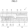
- FIG. 3 is a schematic cross-sectional view of a liquid crystal display device including a transistor according to example embodiments
- a semiconductor layer 4 may be formed over a transistor 10.
- a drain electrode 17b of the transistor 10 may be connected to an electrode 7.
- a liquid crystal layer 8 may be formed on the semiconductor layer 4 and the electrode 7.
- a transparent electrode 9 may be formed over the electrode 7.
- a glass plate 15 may be formed over the transparent electrode 9 and the liquid crystal layer 8. The electrode 7, the liquid crystal layer 8, the transparent electrode 9, and the glass plate 15 collectively form a liquid crystal display portion 13.
- the transistor 10 and the liquid crystal display portion 13 collectively form a liquid crystal display device 1.
- the materials used to form the liquid crystal display portion 13 may be selected from materials well-known in the semiconductor art.
- FIG. 3 depicts a liquid crystal display device including a transistor wherein the active layer 18 includes an organic semiconductor polymer
- the organic semiconductor polymers are applicable to any electronic device.
- the electronic device may be, for example, a memory device, an organic light emitting diode (OLED), an electronic paper (e-paper), a radio-frequency identification (RFID) tag, a flat-panel display including an active-matrix flat-panel display (AMFPD), or a sensor including a photosensor, a biosensor, a chemical sensor or combinations thereof ( e.g., a biochemical sensor, photochemical sensor, etc.), a laser device, a photovoltaic device (e.g., a solar cell) and similar devices.
- OLED organic light emitting diode
- e-paper electronic paper
- RFID radio-frequency identification
- AMFPD active-matrix flat-panel display
- a sensor including a photosensor, a biosensor, a chemical sensor or combinations thereof (e.g., a biochemical sensor
- 2-bromo-3-dodecylthiophene (compound (1), 19.0-g, 57.5-mmol) is reacted with an excessive amount (10.3-g, 115.0-mmol) of copper cyanide (CuCN) to provide 2-cyano-3-dodecylthiophene (compound (2), yield: 71 %).
- the obtained 2-cyano-3-dodecylthiophene and a small amount (about 0.1 equivalents) of diethylamine are dissolved in dimethylformamide (DMF), and then bubbled with H 2 S gas at -70°C for about 40 minutes. The mixture is heated and reacted at about 60°C for 2 hours.
- DMF dimethylformamide
- a nickel (0) compound Ni(cod) 2 , 1.044-g, 3.8-mmol
- bipyridine bpy, 0.59-g, 3.8-mmol
- cyclo-octadiene (0.45-g) are introduced into anhydrous DMF (10-mL) in a reactor under a nitrogen atmosphere and stirred at 60°C for 30 minutes.
- the compound (5) (1.10-g, 1.9-mmol) is added thereto and stirred at about 80°C to 90°C for about 48 hours.
- the reaction solution is added to an ammonia water/methanol (1/2, ca. 1.2-L) mixed solution at room temperature and stirred for 12 hours to complete the reaction. Then, the mixture is filtered under reduced pressure.
- FT-IR (KBr, cm -1 ) 2920, 2846, 1541, 1446, 1394, 1386, 1253, 1232, 1024, 964, 883, 844, 825, 721, 594.
- the thiazole-included compound (7) (0.5-g, 0.43-mmol, 1.0 equivalent) obtained from Example 1-1 and bis(trimethylstannyl)thiophene obtained from the method disclosed in Pham et al. (J. Org. Chem, 1984, Vol. 49, 5250 , 0.16 g, 0.32 mmol, 0.7 equivalents) are introduced into a reactor under the nitrogen atmosphere and completely dissolved in anhydrous DMF with slight heating.
- a polymerization catalyst of tetrakis(triphenylphosphine) palladium (0) (Pd(PPh 3 ) 4 )) (39-mg, 10-mol% relative to compound (7)) is added thereto and reacted at 85°C for 5 hours to 6 hours.
- An excessive amount (1.1-g, 4.3-mmol) of 4-trimethylstannyl-fluorophenyl relative to compound (7) is added thereto and reacted for about 24 hours.
- the mixed reaction solution that has cooled to room temperature is filtered.
- the number average molecular weight measured by GPC is 20,000, and n indicates a polymerization degree.
- FIG. 4 shows 1 H NMR spectra of the Poly-1 polymer (i.e., the polymer having Chemical Formula (21)) according to Example 1 and the Poly-1A polymer (i.e., the polymer having Chemical Formula (21A)) according to Comparative Example 1.
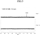
- FIG. 5 shows 19 F NMR spectra of the Poly-1 polymer ( i.e., the polymer having Chemical Formula (21)) according to Example 1 and the Poly-1A polymer ( i.e., the polymer having Chemical Formula (21A)) according to Comparative Example 1. It is confirmed that the Poly-1 polymer obtained in Example 1 has a terminal functional group of fluorophenyl (-C 6 H 4 F) group as shown in FIG. 4 and FIG. 5 .
- the thiazole-included compound (8) (0.25-g, 0.2-mmol, 1.0 equivalent) and bis(trimethylstannyl)thiophene (0.07-g, 0.15-mmol) obtained from the method disclosed in Pham et al. (J. Org. Chem, 1984, Vol. 49, p. 5250 ) are introduced into a reactor under the nitrogen atmosphere and completely dissolved in anhydrous DMF with slight heating. Then, a polymerization catalyst of tetrakis(triphenylphosphine) palladium (0) (Pd(PPh3)4)) (23-mg, 10-mol% relative to the compound (8)) is added thereto and reacted at 85°C for 5 hours to 6 hours.
- Pd(PPh3)4 tetrakis(triphenylphosphine) palladium (0)
- Chemical Formula (33) the number average molecular weight measured by GPC (gel permeation chromatography) is 20,000, and n indicates a polymerization degree.
- FIG. 6 shows a 19 F NMR spectrum of the Poly-2 according to Example 2.
- Example 2 has a terminal functional group of fluorothiophenyl group as shown in FIG. 6 .
- the number average molecular weight measured by GPC is 25,000, and n indicates a polymerization degree.
- 1 H NMR 300MHz, CDCl3) ⁇ 0.85(-CH3), 1.24(-(CH2)9-), 1.46(-CH2-), 1.74(-CH2-), 2.72(Aromatic-CH2-), 2.89(Aromatic-CH2-), 7.05, 7.11, 7.17. 7.33, 7.54, 7.89(-C6H4-CF3), 19 F NMR (300MHz, CDCl3) ⁇ -63.8 (Ph-CF3)
- Chemical Formula (35) the number average molecular weight measured by GPC (gel permeation chromatography) is 41,000, and n indicates a polymerization degree.
- a polymerization catalyst of tetrakis(triphenylphosphine) palladium (0) (Pd(PPh 3 ) 4 )) (25-mg, 10 mol% relative to 5,5'-dibromo-4,4'- bis(dodecyl)-2,2'dithiophene) is added thereto and reacted at 85°C for 5 hours to 6 hours.
- An excessive amount (0.58-g, 2.25-mmol) of 4-trimethylstannyl-fluorophenyl relative to 5,5'-dibromo-4,4'-bis(dodecyl)-2,2'dithiophene is added thereto and reacted for about 24 hours.
- Chemical Formula (36) the number average molecular weight measured by GPC (gel permeation chromatography) is 18,000, and n indicates a polymerization degree.
- a gate electrode 14 of chromium is deposited at 1000- ⁇ on a cleaned glass substrate 12 by sputtering, and an insulation layer 16 of SiO 2 is deposited thereon at 3000- ⁇ by a CVD method.
- Gold (Au) is deposited at 700- ⁇ thereon by sputtering to provide a source electrode 17a and a drain electrode 17b.
- the glass substrate 12 is washed for 10 minutes using isopropyl alcohol, and dried before coating the organic semiconductor material.
- the insulation layer of SiO 2 is treated with UV/O 3 for 30 minutes before the surface modification.
- the device is dipped in octyltrichloro silane solution that is diluted in n-hexane at a concentration of 10-mM for 30 minutes, and the device is washed with hexane and alcohol and dried.
- the Poly-1 polymer represented by Chemical Formula (21) obtained from Example 1 is dissolved in chlorobenzene to a concentration of 1.0-wt% and coated on the device by spin-coating, and then baked at 150°C for one hour under the nitrogen atmosphere to provide an active layer 18, forming an OTFT device 10 having a structure shown in FIG. 1 .
- An OTFT device 10 is manufactured in accordance with the same procedure as in Example 6, except that the active layer 18 includes the organic semiconductor polymer represented by Chemical Formula (21A) obtained from Comparative Example 1.
- 4200-SCS semiconductor characterization system manufactured by KEITHLEY
- FIG. 7 shows that the device has increased electrical stability with a voltage difference ( ⁇ Vth) of 2V or less.
- the OTFT device according to Comparative Example 2 shows similar characteristics (3V or less) thereto ( FIG. 8 ).
- VCS bias voltage
- 4200-SCS semiconductor characterization system manufactured by KEITHLEY
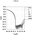
- FIGS. 9 and 10 The results are shown in FIGS. 9 and 10 , respectively.
- the OTFT device according to Example 6 has high stability with a voltage difference ( ⁇ Vth) of 3V or less, but as shown in FIG. 10 , the OTFT device according to Comparative Example 2 has low stability with a voltage difference ( ⁇ Vth) of about 20V.
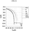
- the OTFT device according to Comparative Example 2 is measured for off-state current transfer characteristics under a nitrogen atmosphere.
- FIG. 11 shows that the OTFT device has low stability with a voltage difference ( ⁇ Vth) of about 20V, similar to that measured in the air. From the results of FIG. 11 , it is considered that the voltage difference of about 20V of the OTFT device is determined by the inherent characteristics of the semiconductor material.
- the organic semiconductor polymers according to example embodiments are capped on the ends by a fluorine-containing group to increase electrical and ambient air stability, and/or charge mobility.
- the organic semiconductor polymers include a thiophene moiety.
- the organic semiconductor polymers may be applied to a channel region of a thin film transistor (TFT).
Landscapes
- Chemical & Material Sciences (AREA)
- Engineering & Computer Science (AREA)
- Materials Engineering (AREA)
- Health & Medical Sciences (AREA)
- Chemical Kinetics & Catalysis (AREA)
- Medicinal Chemistry (AREA)
- Polymers & Plastics (AREA)
- Organic Chemistry (AREA)
- Thin Film Transistor (AREA)
- Polyoxymethylene Polymers And Polymers With Carbon-To-Carbon Bonds (AREA)
Claims (10)
- Organisches Halbleiterpolymer, dargestellt durch die folgende chemische Formel (1):
 G1 und G2 die gleichen oder unterschiedlich sind und unabhängig voneinander ausgewählt sind aus der Gruppe bestehend aus -O-, -S-, -Se-, -CR3R4-CR5R6-, -CR7 =CR8-, und -CR9 =N-, wo R3 bis R9 die gleichen oder unterschiedlich sind und unabhängig voneinander ausgewählt sind aus der Gruppe bestehend aus Wasserstoff, einem Fluor, einem linearen oder verzweigten C1- bis C30-Alkyl, einem C3- bis C30-Cycloalkyl, einem teilfluorierten C1- bis C20-Alkyl, einem C1- bis C20-Perfluoralkyl (CnF2n+1), einem linearen oder verzweigten C1- bis C30-Alkoxy, einem C3- bis C30-Cycloalkoxy, einem linearen oder verzweigten C2- bis C30-Alkoxyalkyl, einem C4- bis C30-Cycloalkoxyalkyl und Kombinationen davon,R1 und R2 die gleichen oder unterschiedlich sind und unabhängig voneinander ausgewählt sind aus der Gruppe bestehend aus Wasserstoff, einem Fluor, einem linearen oder verzweigten C1-bis C30-Alkyl, einem C3- bis C30-Cycloalkyl, einem teilfluorierten C1- bis C20-Alkyl, einem C1-bis C20-Perfluoralkyl (CnF2n+1), einem linearen oder verzweigten C1- bis C30-Alkoxy, einem C3-bis C30-Cycloalkoxy, einem linearen oder verzweigten C2- bis C30-Alkoxyalkyl, einem C4- bis C30-Cycloalkoxyalkyl und Kombinationen davon,n ein Polymerisationsgrad ist und eine ganze Zahl von 8 oder mehr, und a und b unabhängig voneinander ganze Zahlen im Bereich von 1 bis 3 sind, mit der Massgabe, wenn G1 und G2 -O-, -S- oder -Se- sind, zumindest eines von R1 und R2 ein Fluor oder ein C1- bis C20-Perfluoralkyl ist, und mit der Massgabe, wenn G1 und G2 -CR3R4-CR5R6-, -CR7 =CR8- oder -CR9 =N- sind, zumindest eines von R1 bis R9 ein Fluor oder ein C1- bis C20-Perfluoralkyl ist, undAr durch eine der folgenden chemischen Formeln (2), (5) und (6) dargestellt wird:
 R11 Wasserstoff oder ein C1- bis C20-Alkyl ist,Ar1 ausgewählt ist aus der Gruppe bestehend aus funktionellen Gruppen, dargestellt durch die chemischen Formeln (3-1) bis (3-27), Thiadiazol, Oxadiazol, Pyrazole, Triazole, Tetrazol, Pyridazin, Isochinolin, Naphthyridin, Pyrimidopyrimidin, Pyridopyrimidin, Benzothiazol, Benzooxazol, Phenanthridin,
 wobei, in den chemischen Formeln (3-1) bis (3-27), Y Wasserstoff, ein lineares oder verzweigtes C1- bis C20-Alkyl, ein C3- bis C20-Cycloalkyl, ein C6- bis C30-Aryl, ein lineares oder verzweigtes C1- bis C16-Alkoxy oder ein C3- bis C16-Cycloalkoxyalkyl ist,x eine ganze Zahl im Bereich von 1 bis 12, undy eine ganze Zahl im Bereich von 1 bis 4 ist;
 Xb und Xc N sind,Y1 und Y2 die gleichen oder unterschiedlich sind und unabhängig voneinander S oder Se sind,R14 bis R19 die gleichen oder unterschiedlich sind und unabhängig voneinander Wasserstoff oder ein C1- bis C20-Alkyl sind und m 0 bis 2 ist;
 R20, R'20, R21, und R'21 die gleichen oder unterschiedlich sind und unabhängig voneinander Wasserstoff oder ein C1- bis C20-Alkyl sind, oderdas organische Halbleiterpolymer durch eine der folgenden chemischen Formeln (11)-(37) dargestellt wird:
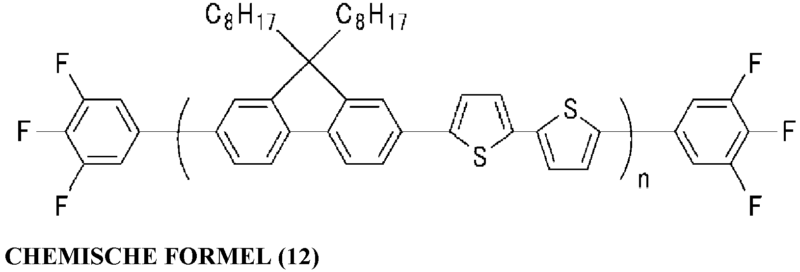


- Organisches Halbleiterpolymer nach Anspruch 1, wobei R3 bis R9 die gleichen oder unterschiedlich sind und unabhängig voneinander ausgewählt sind aus der Gruppe bestehend aus dem Fluor, dem teilfluorierten C1- bis C20-Alkyl, dem C1- bis C20-Perfluoralkyl (CnF2n+1) und Kombinationen davon.
- Organisches Halbleiterpolymer nach Anspruch 1 oder 2, wobei R1 und R2 die gleichen oder unterschiedlich sind und unabhängig voneinander ausgewählt sind aus der Gruppe bestehend aus dem Fluor, dem teilfluorierten C1- bis C20-Alkyl, dem C1- bis C20-Perfluoralkyl (CnF2n+1) und Kombinationen davon.
- Organisches Halbleiterpolymer nach Anspruch 1, wobei das organische Halbleiterpolymer ein Polymer vom p-Typ ist.
- Organisches Halbleiterpolymer nach Anspruch 1, wobei Ar durch die chemische Formel (5-1) dargestellt wird:

R'14 bis R'19 die gleichen oder unterschiedlich sind und unabhängig voneinander Wasserstoff oder ein C1- bis C20-Alkyl sind. - Organisches Halbleiterpolymer nach Anspruch 1, wobei Ar durch die chemische Formel (6-1) dargestellt wird:

R20 und R'20 die gleichen oder unterschiedlich sind und unabhängig voneinander Wasserstoff oder ein C1- bis C20-Alkyl sind. - Organisches Halbleiterpolymer nach einem der Ansprüche 1-6, wobei das organische Halbleiterpolymer eine funktionelle Endgruppe enthält, die durch eine der folgenden chemischen Formeln (7) bis (10) dargestellt wird:

R ein Fluor oder ein C1- bis C20-Perfluoralkyl ist und a eine ganze Zahl im Bereich von 1 bis 5 ist,
R ein Fluor oder ein C1- bis C20-Perfluoralkyl ist und a eine ganze Zahl im Bereich von 1 bis 6 ist,
R ein Fluor oder ein C1- bis C20-Perfluoralkyl ist und a eine ganze Zahl im Bereich von 1 bis 3 ist, und
R ein Fluor oder ein C1- bis C20-Perfluoralkyl ist und a eine ganze Zahl im Bereich von 1 bis 3 ist. - Transistor, umfassen das organische Halbleiterpolymer nach einem der Ansprüche 1-7.
- Transistor nach Anspruch 8, ferner umfassend:eine Gate-Elektrode;eine Source-Elektrode und eine Drain-Elektrode, die einander zugewandt sind und eine Kanalregion definieren;eine Isolierschicht, die die Source-Elektrode, Drain-Elektrode und die Gate-Elektrode elektrisch isoliert, undeine aktive Schicht, enthaltend das organische Halbleiterpolymer in der Kanalregion.
- Elektronische Vorrichtung, umfassend zumindest eines der organischen Halbleiterpolymer nach einem der Ansprüche 1-7 und den Transistor nach Anspruch 8 oder 9.
Applications Claiming Priority (1)
| Application Number | Priority Date | Filing Date | Title |
|---|---|---|---|
| KR1020090060880A KR101648072B1 (ko) | 2009-07-03 | 2009-07-03 | 유기 반도체 고분자 및 이를 포함하는 트랜지스터 |
Publications (2)
| Publication Number | Publication Date |
|---|---|
| EP2270064A1 EP2270064A1 (de) | 2011-01-05 |
| EP2270064B1 true EP2270064B1 (de) | 2020-02-19 |
Family
ID=43012538
Family Applications (1)
| Application Number | Title | Priority Date | Filing Date |
|---|---|---|---|
| EP10167763.1A Active EP2270064B1 (de) | 2009-07-03 | 2010-06-29 | Organisches Halbleiterpolymer, Transistor mit einem organischen Halbleiterpolymer und Herstellungsverfahren dafür |
Country Status (4)
| Country | Link |
|---|---|
| US (1) | US8809839B2 (de) |
| EP (1) | EP2270064B1 (de) |
| KR (1) | KR101648072B1 (de) |
| CN (1) | CN101942075B (de) |
Families Citing this family (8)
| Publication number | Priority date | Publication date | Assignee | Title |
|---|---|---|---|---|
| KR101648072B1 (ko) | 2009-07-03 | 2016-08-12 | 삼성전자 주식회사 | 유기 반도체 고분자 및 이를 포함하는 트랜지스터 |
| KR101730617B1 (ko) * | 2010-11-22 | 2017-04-27 | 삼성전자주식회사 | 유기 반도체 소자용 조성물 및 이로부터 얻어지는 고분자를 포함하는 트랜지스터와 전자 소자 |
| US8936965B2 (en) * | 2010-11-26 | 2015-01-20 | Semiconductor Energy Laboratory Co., Ltd. | Semiconductor device and manufacturing method thereof |
| KR102011872B1 (ko) * | 2011-01-04 | 2019-08-19 | 삼성전자주식회사 | 낮은 밴드 갭을 갖는 유기 반도체 화합물 및 이를 포함하는 트랜지스터와 전자 소자 |
| KR20130058542A (ko) * | 2011-11-25 | 2013-06-04 | 삼성전자주식회사 | 유기 반도체 화합물 및 이를 포함하는 유기 박막 |
| KR20130085860A (ko) | 2012-01-20 | 2013-07-30 | 삼성전자주식회사 | 유기 전자 소자 |
| ES2909109T3 (es) * | 2015-03-26 | 2022-05-05 | Next Energy Tech Inc | Compuestos colorantes fluorados para células solares orgánicas |
| CN115584017B (zh) * | 2022-09-30 | 2024-10-11 | 武汉工程大学 | 一类联二噻唑类宽带隙聚合物及其在光电器件中的应用 |
Citations (3)
| Publication number | Priority date | Publication date | Assignee | Title |
|---|---|---|---|---|
| WO2002009201A1 (en) * | 2000-07-24 | 2002-01-31 | Northwestern University | n-TYPE THIOPHENE SEMICONDUCTORS |
| WO2003010778A1 (en) * | 2001-07-24 | 2003-02-06 | Northwestern University | n-TYPE THIOPHENE SEMICONDUCTORS |
| WO2008111461A1 (ja) * | 2007-03-09 | 2008-09-18 | Sumitomo Chemical Company, Limited | 含フッ素多環芳香族化合物、含フッ素重合体、有機薄膜及び有機薄膜素子 |
Family Cites Families (21)
| Publication number | Priority date | Publication date | Assignee | Title |
|---|---|---|---|---|
| JPH02202514A (ja) * | 1989-01-31 | 1990-08-10 | Nippon Oil & Fats Co Ltd | フルオロアルキル基含有ヘテロ芳香族系重合体 |
| JPH0414906A (ja) * | 1990-05-08 | 1992-01-20 | Matsushita Electric Ind Co Ltd | フェーダ切替装置 |
| FI95574C (fi) | 1994-02-16 | 1996-02-26 | Valtion Teknillinen | Elektroneja johtavia molekyylivalmisteita |
| US5946551A (en) | 1997-03-25 | 1999-08-31 | Dimitrakopoulos; Christos Dimitrios | Fabrication of thin film effect transistor comprising an organic semiconductor and chemical solution deposited metal oxide gate dielectric |
| GB9726810D0 (en) * | 1997-12-19 | 1998-02-18 | Zeneca Ltd | Compounds composition & use |
| US6215130B1 (en) | 1998-08-20 | 2001-04-10 | Lucent Technologies Inc. | Thin film transistors |
| US6166172A (en) | 1999-02-10 | 2000-12-26 | Carnegie Mellon University | Method of forming poly-(3-substituted) thiophenes |
| KR101069519B1 (ko) | 2004-07-08 | 2011-09-30 | 삼성전자주식회사 | 올리고티오펜과 n-형 방향족 화합물을 주쇄에 교호로 포함하는 유기 반도체 고분자 |
| US7528176B2 (en) | 2004-09-14 | 2009-05-05 | Northwestern University | Carbonyl-functionalized thiophene compounds and related device structures |
| KR20060056824A (ko) | 2004-11-22 | 2006-05-25 | 오성근 | 전도성 고분자 제조에 있어서 도핑제로 황이 함유된유기물 염에 금속 이온 또는 나노 입자를 결합시켜이용하는 기술 |
| KR100786865B1 (ko) * | 2005-12-26 | 2007-12-20 | 삼성에스디아이 주식회사 | 광전변환 소자 |
| JP2007197358A (ja) * | 2006-01-26 | 2007-08-09 | Sumitomo Seika Chem Co Ltd | (チオフェン/フェニレン)コオリゴマーおよびそれらを含む発光材料 |
| EP2192123B1 (de) * | 2006-03-10 | 2012-11-21 | Sumitomo Chemical Company, Limited | Fusionerte tricyklische verbindungen sowie ihre verwendung in geräte mit organischem dünnen film, z.b transistoren |
| JP2008097949A (ja) | 2006-10-11 | 2008-04-24 | Japan Aviation Electronics Industry Ltd | 導電性ペースト |
| JP5039998B2 (ja) | 2007-01-15 | 2012-10-03 | ダイキン工業株式会社 | 含フッ素チオフェン重合体 |
| DE102007004862B4 (de) | 2007-01-31 | 2014-01-30 | Globalfoundries Inc. | Verfahren zur Herstellung von Si-Ge enthaltenden Drain/Source-Gebieten in Transistoren mit geringerem Si/Ge-Verlust |
| WO2008144750A1 (en) | 2007-05-21 | 2008-11-27 | Plextronics, Inc. | Porphyrin and conductive polymer compositions for use in solid-state electronic devices |
| US7816426B2 (en) * | 2007-07-16 | 2010-10-19 | Evonik Stockhausen, Llc | Superabsorbent polymer compositions having color stability |
| KR20090113990A (ko) | 2008-04-29 | 2009-11-03 | 한양대학교 산학협력단 | 전도성 폴리아닐린 나노입자의 제조방법 및 이에 의하여제조된 전도성 폴리아닐린 나노입자 |
| KR101580318B1 (ko) | 2008-05-14 | 2015-12-28 | 삼성전자주식회사 | 나노 금속 결합용 단량체, 전도성 고분자 복합체 및 그의제조방법 |
| KR101648072B1 (ko) | 2009-07-03 | 2016-08-12 | 삼성전자 주식회사 | 유기 반도체 고분자 및 이를 포함하는 트랜지스터 |
-
2009
- 2009-07-03 KR KR1020090060880A patent/KR101648072B1/ko active Active
-
2010
- 2010-06-29 EP EP10167763.1A patent/EP2270064B1/de active Active
- 2010-07-05 CN CN201010222301.0A patent/CN101942075B/zh active Active
- 2010-07-06 US US12/801,959 patent/US8809839B2/en active Active
Patent Citations (4)
| Publication number | Priority date | Publication date | Assignee | Title |
|---|---|---|---|---|
| WO2002009201A1 (en) * | 2000-07-24 | 2002-01-31 | Northwestern University | n-TYPE THIOPHENE SEMICONDUCTORS |
| WO2003010778A1 (en) * | 2001-07-24 | 2003-02-06 | Northwestern University | n-TYPE THIOPHENE SEMICONDUCTORS |
| WO2008111461A1 (ja) * | 2007-03-09 | 2008-09-18 | Sumitomo Chemical Company, Limited | 含フッ素多環芳香族化合物、含フッ素重合体、有機薄膜及び有機薄膜素子 |
| EP2133321A1 (de) * | 2007-03-09 | 2009-12-16 | Sumitomo Chemical Company, Limited | Fluorhaltige polycyclische aromatische verbindung, fluorhaltiges polymer, organischer dünner film und gerät mit organischem dünnen film |
Non-Patent Citations (3)
| Title |
|---|
| A. FACCHETTI ET AL: "n-Type Building Blocks for Organic Electronics: A Homologous Family of Fluorocarbon-Substituted Thiophene Oligomers with High Carrier Mobility", ADVANCED MATERIALS, vol. 15, no. 1, 3 January 2003 (2003-01-03), DE, pages 33 - 38, XP055469711, ISSN: 0935-9648, DOI: 10.1002/adma.200390003 * |
| LI L ET AL: "TUNING THE ELECTRONIC STRUCTURE OF CONJUGATED POLYMERS WITH FLUOROALKYL SUBSTITUTION: ALTERNATING ALKYL/PERFLUOROALKYL-SUBSTITUTED POLYTHIOPHENE", MACROMOLECULES, AMERICAN CHEMICAL SOCIETY, US, vol. 38, no. 2, 25 January 2005 (2005-01-25), pages 372 - 378, XP001225256, ISSN: 0024-9297, DOI: 10.1021/MA048510R * |
| NEWMAN C R ET AL: "Introduction to Organic thin film transistors and design of n-channel organic semiconductors", CHEMISTRY OF MATERIALS, AMERICAN CHEMICAL SOCIETY, US, vol. 16, no. 23, 1 January 2004 (2004-01-01), pages 4436 - 4451, XP002478736, ISSN: 0897-4756, [retrieved on 20040831], DOI: 10.1021/CM049391X * |
Also Published As
| Publication number | Publication date |
|---|---|
| CN101942075B (zh) | 2014-09-17 |
| US8809839B2 (en) | 2014-08-19 |
| KR20110003221A (ko) | 2011-01-11 |
| KR101648072B1 (ko) | 2016-08-12 |
| US20110001131A1 (en) | 2011-01-06 |
| CN101942075A (zh) | 2011-01-12 |
| EP2270064A1 (de) | 2011-01-05 |
Similar Documents
| Publication | Publication Date | Title |
|---|---|---|
| US8354666B2 (en) | Organic polymer semiconductor, method of preparing the same, and ambipolar organic thin film transistor using the same | |
| US8008426B2 (en) | Organic semiconductor polymer having liquid crystal properties, organic active layer, organic thin film transistor, and electronic device including the same, and methods of fabricating the same | |
| US7030409B2 (en) | Organic semiconductor polymer for organic thin film transistor containing quinoxaline ring in the backbone chain | |
| EP2270064A1 (de) | Organisches Halbleiterpolymer, Transistor mit einem organischen Halbleiterpolymer und Herstellungsverfahren dafür | |
| EP2474551B1 (de) | Organische Halbleiterverbindung, diese enthaltender Transistor und elektronische Vorrichtung | |
| EP2083033B1 (de) | Organisches halbleitendes Copolymer und organische Elektrovorrichtung damit | |
| EP2472625B1 (de) | Organische Halbleiterverbindungen mit geringen Bandabständen sowie elektronische Vorrichtungen damit | |
| KR101888617B1 (ko) | 유기 반도체 화합물, 이를 포함하는 유기 박막, 상기 유기 박막을 포함하는 전자 소자 및 유기 박막의 제조방법 | |
| US8933441B2 (en) | Organic electronic device | |
| US8154016B2 (en) | Composition containing thiazole rings, organic semiconductor polymer containing the composition, organic active layer containing the organic semiconductor polymer, organic thin film transistor containing the organic active layer, electronic device containing the organic thin film transistor and method of preparing the same | |
| US8405071B2 (en) | Organic semiconductor polymer and transistor including the same | |
| KR101935466B1 (ko) | 유기 전자 소자 | |
| KR101675073B1 (ko) | 유기 반도체 고분자 및 이를 포함하는 트랜지스터와 전자 소자 | |
| US20060151779A1 (en) | Novel thiophene-thiazole derivatives and organic thin film transistors using the same | |
| KR101947020B1 (ko) | 낮은 밴드 갭을 갖는 유기 반도체 화합물 및 이를 포함하는 트랜지스터와 전자 소자 | |
| US9790236B2 (en) | Organic semiconductor compound, and transistor and electronic device including the same |
Legal Events
| Date | Code | Title | Description |
|---|---|---|---|
| PUAI | Public reference made under article 153(3) epc to a published international application that has entered the european phase |
Free format text: ORIGINAL CODE: 0009012 |
|
| AK | Designated contracting states |
Kind code of ref document: A1 Designated state(s): AL AT BE BG CH CY CZ DE DK EE ES FI FR GB GR HR HU IE IS IT LI LT LU LV MC MK MT NL NO PL PT RO SE SI SK SM TR |
|
| AX | Request for extension of the european patent |
Extension state: BA ME RS |
|
| 17P | Request for examination filed |
Effective date: 20110705 |
|
| RAP1 | Party data changed (applicant data changed or rights of an application transferred) |
Owner name: SAMSUNG ELECTRONICS CO., LTD. |
|
| 17Q | First examination report despatched |
Effective date: 20150420 |
|
| STAA | Information on the status of an ep patent application or granted ep patent |
Free format text: STATUS: EXAMINATION IS IN PROGRESS |
|
| GRAP | Despatch of communication of intention to grant a patent |
Free format text: ORIGINAL CODE: EPIDOSNIGR1 |
|
| STAA | Information on the status of an ep patent application or granted ep patent |
Free format text: STATUS: GRANT OF PATENT IS INTENDED |
|
| INTG | Intention to grant announced |
Effective date: 20190830 |
|
| GRAS | Grant fee paid |
Free format text: ORIGINAL CODE: EPIDOSNIGR3 |
|
| GRAA | (expected) grant |
Free format text: ORIGINAL CODE: 0009210 |
|
| STAA | Information on the status of an ep patent application or granted ep patent |
Free format text: STATUS: THE PATENT HAS BEEN GRANTED |
|
| AK | Designated contracting states |
Kind code of ref document: B1 Designated state(s): AL AT BE BG CH CY CZ DE DK EE ES FI FR GB GR HR HU IE IS IT LI LT LU LV MC MK MT NL NO PL PT RO SE SI SK SM TR |
|
| REG | Reference to a national code |
Ref country code: GB Ref legal event code: FG4D |
|
| REG | Reference to a national code |
Ref country code: CH Ref legal event code: EP |
|
| REG | Reference to a national code |
Ref country code: DE Ref legal event code: R096 Ref document number: 602010063131 Country of ref document: DE |
|
| REG | Reference to a national code |
Ref country code: AT Ref legal event code: REF Ref document number: 1234905 Country of ref document: AT Kind code of ref document: T Effective date: 20200315 |
|
| REG | Reference to a national code |
Ref country code: IE Ref legal event code: FG4D |
|
| REG | Reference to a national code |
Ref country code: NL Ref legal event code: MP Effective date: 20200219 |
|
| PG25 | Lapsed in a contracting state [announced via postgrant information from national office to epo] |
Ref country code: FI Free format text: LAPSE BECAUSE OF FAILURE TO SUBMIT A TRANSLATION OF THE DESCRIPTION OR TO PAY THE FEE WITHIN THE PRESCRIBED TIME-LIMIT Effective date: 20200219 Ref country code: NO Free format text: LAPSE BECAUSE OF FAILURE TO SUBMIT A TRANSLATION OF THE DESCRIPTION OR TO PAY THE FEE WITHIN THE PRESCRIBED TIME-LIMIT Effective date: 20200519 |
|
| REG | Reference to a national code |
Ref country code: LT Ref legal event code: MG4D |
|
| PG25 | Lapsed in a contracting state [announced via postgrant information from national office to epo] |
Ref country code: BG Free format text: LAPSE BECAUSE OF FAILURE TO SUBMIT A TRANSLATION OF THE DESCRIPTION OR TO PAY THE FEE WITHIN THE PRESCRIBED TIME-LIMIT Effective date: 20200519 Ref country code: IS Free format text: LAPSE BECAUSE OF FAILURE TO SUBMIT A TRANSLATION OF THE DESCRIPTION OR TO PAY THE FEE WITHIN THE PRESCRIBED TIME-LIMIT Effective date: 20200619 Ref country code: GR Free format text: LAPSE BECAUSE OF FAILURE TO SUBMIT A TRANSLATION OF THE DESCRIPTION OR TO PAY THE FEE WITHIN THE PRESCRIBED TIME-LIMIT Effective date: 20200520 Ref country code: LV Free format text: LAPSE BECAUSE OF FAILURE TO SUBMIT A TRANSLATION OF THE DESCRIPTION OR TO PAY THE FEE WITHIN THE PRESCRIBED TIME-LIMIT Effective date: 20200219 Ref country code: SE Free format text: LAPSE BECAUSE OF FAILURE TO SUBMIT A TRANSLATION OF THE DESCRIPTION OR TO PAY THE FEE WITHIN THE PRESCRIBED TIME-LIMIT Effective date: 20200219 Ref country code: HR Free format text: LAPSE BECAUSE OF FAILURE TO SUBMIT A TRANSLATION OF THE DESCRIPTION OR TO PAY THE FEE WITHIN THE PRESCRIBED TIME-LIMIT Effective date: 20200219 |
|
| PG25 | Lapsed in a contracting state [announced via postgrant information from national office to epo] |
Ref country code: NL Free format text: LAPSE BECAUSE OF FAILURE TO SUBMIT A TRANSLATION OF THE DESCRIPTION OR TO PAY THE FEE WITHIN THE PRESCRIBED TIME-LIMIT Effective date: 20200219 |
|
| PG25 | Lapsed in a contracting state [announced via postgrant information from national office to epo] |
Ref country code: SK Free format text: LAPSE BECAUSE OF FAILURE TO SUBMIT A TRANSLATION OF THE DESCRIPTION OR TO PAY THE FEE WITHIN THE PRESCRIBED TIME-LIMIT Effective date: 20200219 Ref country code: PT Free format text: LAPSE BECAUSE OF FAILURE TO SUBMIT A TRANSLATION OF THE DESCRIPTION OR TO PAY THE FEE WITHIN THE PRESCRIBED TIME-LIMIT Effective date: 20200712 Ref country code: DK Free format text: LAPSE BECAUSE OF FAILURE TO SUBMIT A TRANSLATION OF THE DESCRIPTION OR TO PAY THE FEE WITHIN THE PRESCRIBED TIME-LIMIT Effective date: 20200219 Ref country code: SM Free format text: LAPSE BECAUSE OF FAILURE TO SUBMIT A TRANSLATION OF THE DESCRIPTION OR TO PAY THE FEE WITHIN THE PRESCRIBED TIME-LIMIT Effective date: 20200219 Ref country code: LT Free format text: LAPSE BECAUSE OF FAILURE TO SUBMIT A TRANSLATION OF THE DESCRIPTION OR TO PAY THE FEE WITHIN THE PRESCRIBED TIME-LIMIT Effective date: 20200219 Ref country code: EE Free format text: LAPSE BECAUSE OF FAILURE TO SUBMIT A TRANSLATION OF THE DESCRIPTION OR TO PAY THE FEE WITHIN THE PRESCRIBED TIME-LIMIT Effective date: 20200219 Ref country code: RO Free format text: LAPSE BECAUSE OF FAILURE TO SUBMIT A TRANSLATION OF THE DESCRIPTION OR TO PAY THE FEE WITHIN THE PRESCRIBED TIME-LIMIT Effective date: 20200219 Ref country code: ES Free format text: LAPSE BECAUSE OF FAILURE TO SUBMIT A TRANSLATION OF THE DESCRIPTION OR TO PAY THE FEE WITHIN THE PRESCRIBED TIME-LIMIT Effective date: 20200219 Ref country code: CZ Free format text: LAPSE BECAUSE OF FAILURE TO SUBMIT A TRANSLATION OF THE DESCRIPTION OR TO PAY THE FEE WITHIN THE PRESCRIBED TIME-LIMIT Effective date: 20200219 |
|
| REG | Reference to a national code |
Ref country code: AT Ref legal event code: MK05 Ref document number: 1234905 Country of ref document: AT Kind code of ref document: T Effective date: 20200219 |
|
| REG | Reference to a national code |
Ref country code: DE Ref legal event code: R097 Ref document number: 602010063131 Country of ref document: DE |
|
| PLBE | No opposition filed within time limit |
Free format text: ORIGINAL CODE: 0009261 |
|
| STAA | Information on the status of an ep patent application or granted ep patent |
Free format text: STATUS: NO OPPOSITION FILED WITHIN TIME LIMIT |
|
| 26N | No opposition filed |
Effective date: 20201120 |
|
| PG25 | Lapsed in a contracting state [announced via postgrant information from national office to epo] |
Ref country code: MC Free format text: LAPSE BECAUSE OF FAILURE TO SUBMIT A TRANSLATION OF THE DESCRIPTION OR TO PAY THE FEE WITHIN THE PRESCRIBED TIME-LIMIT Effective date: 20200219 Ref country code: IT Free format text: LAPSE BECAUSE OF FAILURE TO SUBMIT A TRANSLATION OF THE DESCRIPTION OR TO PAY THE FEE WITHIN THE PRESCRIBED TIME-LIMIT Effective date: 20200219 Ref country code: AT Free format text: LAPSE BECAUSE OF FAILURE TO SUBMIT A TRANSLATION OF THE DESCRIPTION OR TO PAY THE FEE WITHIN THE PRESCRIBED TIME-LIMIT Effective date: 20200219 |
|
| REG | Reference to a national code |
Ref country code: CH Ref legal event code: PL |
|
| PG25 | Lapsed in a contracting state [announced via postgrant information from national office to epo] |
Ref country code: SI Free format text: LAPSE BECAUSE OF FAILURE TO SUBMIT A TRANSLATION OF THE DESCRIPTION OR TO PAY THE FEE WITHIN THE PRESCRIBED TIME-LIMIT Effective date: 20200219 Ref country code: PL Free format text: LAPSE BECAUSE OF FAILURE TO SUBMIT A TRANSLATION OF THE DESCRIPTION OR TO PAY THE FEE WITHIN THE PRESCRIBED TIME-LIMIT Effective date: 20200219 |
|
| PG25 | Lapsed in a contracting state [announced via postgrant information from national office to epo] |
Ref country code: LU Free format text: LAPSE BECAUSE OF NON-PAYMENT OF DUE FEES Effective date: 20200629 |
|
| REG | Reference to a national code |
Ref country code: BE Ref legal event code: MM Effective date: 20200630 |
|
| PG25 | Lapsed in a contracting state [announced via postgrant information from national office to epo] |
Ref country code: CH Free format text: LAPSE BECAUSE OF NON-PAYMENT OF DUE FEES Effective date: 20200630 Ref country code: IE Free format text: LAPSE BECAUSE OF NON-PAYMENT OF DUE FEES Effective date: 20200629 Ref country code: LI Free format text: LAPSE BECAUSE OF NON-PAYMENT OF DUE FEES Effective date: 20200630 |
|
| PG25 | Lapsed in a contracting state [announced via postgrant information from national office to epo] |
Ref country code: BE Free format text: LAPSE BECAUSE OF NON-PAYMENT OF DUE FEES Effective date: 20200630 |
|
| PG25 | Lapsed in a contracting state [announced via postgrant information from national office to epo] |
Ref country code: TR Free format text: LAPSE BECAUSE OF FAILURE TO SUBMIT A TRANSLATION OF THE DESCRIPTION OR TO PAY THE FEE WITHIN THE PRESCRIBED TIME-LIMIT Effective date: 20200219 Ref country code: MT Free format text: LAPSE BECAUSE OF FAILURE TO SUBMIT A TRANSLATION OF THE DESCRIPTION OR TO PAY THE FEE WITHIN THE PRESCRIBED TIME-LIMIT Effective date: 20200219 Ref country code: CY Free format text: LAPSE BECAUSE OF FAILURE TO SUBMIT A TRANSLATION OF THE DESCRIPTION OR TO PAY THE FEE WITHIN THE PRESCRIBED TIME-LIMIT Effective date: 20200219 |
|
| PG25 | Lapsed in a contracting state [announced via postgrant information from national office to epo] |
Ref country code: MK Free format text: LAPSE BECAUSE OF FAILURE TO SUBMIT A TRANSLATION OF THE DESCRIPTION OR TO PAY THE FEE WITHIN THE PRESCRIBED TIME-LIMIT Effective date: 20200219 Ref country code: AL Free format text: LAPSE BECAUSE OF FAILURE TO SUBMIT A TRANSLATION OF THE DESCRIPTION OR TO PAY THE FEE WITHIN THE PRESCRIBED TIME-LIMIT Effective date: 20200219 |
|
| P01 | Opt-out of the competence of the unified patent court (upc) registered |
Effective date: 20230519 |
|
| PGFP | Annual fee paid to national office [announced via postgrant information from national office to epo] |
Ref country code: DE Payment date: 20250507 Year of fee payment: 16 |
|
| PGFP | Annual fee paid to national office [announced via postgrant information from national office to epo] |
Ref country code: GB Payment date: 20250508 Year of fee payment: 16 |
|
| PGFP | Annual fee paid to national office [announced via postgrant information from national office to epo] |
Ref country code: FR Payment date: 20250508 Year of fee payment: 16 |