EP1434403B1 - Détection d'un décalage de porteuse et synchronisation d'un horloge de trame dans un récepteur de signaux multiporteurs - Google Patents
Détection d'un décalage de porteuse et synchronisation d'un horloge de trame dans un récepteur de signaux multiporteurs Download PDFInfo
- Publication number
- EP1434403B1 EP1434403B1 EP04004148A EP04004148A EP1434403B1 EP 1434403 B1 EP1434403 B1 EP 1434403B1 EP 04004148 A EP04004148 A EP 04004148A EP 04004148 A EP04004148 A EP 04004148A EP 1434403 B1 EP1434403 B1 EP 1434403B1
- Authority
- EP
- European Patent Office
- Prior art keywords
- symbol
- frequency offset
- signal
- integral
- frame clock
- Prior art date
- Legal status (The legal status is an assumption and is not a legal conclusion. Google has not performed a legal analysis and makes no representation as to the accuracy of the status listed.)
- Expired - Lifetime
Links
Images



Classifications
-
- H—ELECTRICITY
- H04—ELECTRIC COMMUNICATION TECHNIQUE
- H04L—TRANSMISSION OF DIGITAL INFORMATION, e.g. TELEGRAPHIC COMMUNICATION
- H04L27/00—Modulated-carrier systems
- H04L27/26—Systems using multi-frequency codes
- H04L27/2601—Multicarrier modulation systems
- H04L27/2647—Arrangements specific to the receiver only
- H04L27/2655—Synchronisation arrangements
- H04L27/2657—Carrier synchronisation
- H04L27/266—Fine or fractional frequency offset determination and synchronisation
-
- H—ELECTRICITY
- H04—ELECTRIC COMMUNICATION TECHNIQUE
- H04L—TRANSMISSION OF DIGITAL INFORMATION, e.g. TELEGRAPHIC COMMUNICATION
- H04L27/00—Modulated-carrier systems
- H04L27/26—Systems using multi-frequency codes
- H04L27/2601—Multicarrier modulation systems
- H04L27/2647—Arrangements specific to the receiver only
- H04L27/2655—Synchronisation arrangements
- H04L27/2656—Frame synchronisation, e.g. packet synchronisation, time division duplex [TDD] switching point detection or subframe synchronisation
-
- H—ELECTRICITY
- H04—ELECTRIC COMMUNICATION TECHNIQUE
- H04L—TRANSMISSION OF DIGITAL INFORMATION, e.g. TELEGRAPHIC COMMUNICATION
- H04L27/00—Modulated-carrier systems
- H04L27/26—Systems using multi-frequency codes
- H04L27/2601—Multicarrier modulation systems
- H04L27/2647—Arrangements specific to the receiver only
- H04L27/2655—Synchronisation arrangements
- H04L27/2657—Carrier synchronisation
- H04L27/2659—Coarse or integer frequency offset determination and synchronisation
-
- H—ELECTRICITY
- H04—ELECTRIC COMMUNICATION TECHNIQUE
- H04L—TRANSMISSION OF DIGITAL INFORMATION, e.g. TELEGRAPHIC COMMUNICATION
- H04L27/00—Modulated-carrier systems
- H04L27/26—Systems using multi-frequency codes
- H04L27/2601—Multicarrier modulation systems
- H04L27/2647—Arrangements specific to the receiver only
- H04L27/2655—Synchronisation arrangements
- H04L27/2662—Symbol synchronisation
-
- H—ELECTRICITY
- H04—ELECTRIC COMMUNICATION TECHNIQUE
- H04L—TRANSMISSION OF DIGITAL INFORMATION, e.g. TELEGRAPHIC COMMUNICATION
- H04L27/00—Modulated-carrier systems
- H04L27/26—Systems using multi-frequency codes
- H04L27/2601—Multicarrier modulation systems
- H04L27/2647—Arrangements specific to the receiver only
- H04L27/2655—Synchronisation arrangements
- H04L27/2668—Details of algorithms
- H04L27/2673—Details of algorithms characterised by synchronisation parameters
- H04L27/2675—Pilot or known symbols
-
- H—ELECTRICITY
- H04—ELECTRIC COMMUNICATION TECHNIQUE
- H04L—TRANSMISSION OF DIGITAL INFORMATION, e.g. TELEGRAPHIC COMMUNICATION
- H04L27/00—Modulated-carrier systems
- H04L27/26—Systems using multi-frequency codes
- H04L27/2601—Multicarrier modulation systems
- H04L27/2647—Arrangements specific to the receiver only
- H04L27/2655—Synchronisation arrangements
- H04L27/2668—Details of algorithms
- H04L27/2673—Details of algorithms characterised by synchronisation parameters
- H04L27/2676—Blind, i.e. without using known symbols
Definitions
- This invention pertains in general to a synchronization method and system for digital receivers and, more particularly, to a method and system for obtaining frame, carrier, and dock synchronization for digital audio broadcasting and digital video broadcasting systems.
- Digital audio broadcasting and digital video broadcasting provide high quality signals with minimal multi-path distortion, noise, or signal drop-offs, as commonly seen in analog broadcasting.
- DAB digital audio broadcasting
- One such standard is the Eureka 147 system.
- Eureka is a research and development consortium of European governments corporations, and universities to develop new technologies. Project number 147, began in 1986, focuses on the DAB technology and seeks to implement the technology under a standardized system for both terrestrial and satellite broadcasting.
- the Eureka 147 system has been adopted in Europe and Canada, and is being considered in the U.S. in conjunction with the "In band, On channel" (“IBOC”) system.
- IBOC In band, On channel
- An audio input signal of the Eureka 147 DAB system is generally encoded with a masking-pattern universal subband integrated coding and multiplexing ("MUSICAM”) to divide a signal into subbands and to minimize hearing threshold and masking to achieve data reduction. Convolutional coding is then performed, followed by re-distribution of data bits in time and frequency, i.e., interleaving, such that the largest error that can occur in a signal block is limited and the ability to correct burst errors is increased.
- the Eureka 147 system uses orthogonal frequency division multiplexing (“OFDM”) with quadrature phase shift keying (“QPSK”) modulation on each carrier to distribute several audio data channels among overlapping carriers. A guard interval is also inserted between data blocks to reduce intersymbol and multipath interference. The modulated DAB signals are then transmitted over multipath channels.
- OFDM orthogonal frequency division multiplexing
- QPSK quadrature phase shift keying
- synchronization for a DAB system at various communication layers is important. Because of various changes in propagation channels for a DAB system, synchronization is difficult, especially for carrier and dock synchronization.
- many algorithms and systems for conventional OFDM systems are incompatible with the Eureka 147 system largely due to the difference in the transmission frame structure of the Eureka system.
- Fouche et al. describe a method and apparatus for realigning local oscillators to lower the complexity of the clock recovery system at the receiver level in U.S. Patent No. 5,313,169, entitled “Method of Realigning the Local Oscillators of a Receiver and Device For Implementing the Method", issued on May 17, 1994.
- the method and device are based on two master lines of the OFDM signal spectrum having a fixed frequency difference between them. This difference is used to calculate the variation of the phases of the lines.
- the frequency spectrum of the Eureka 147 system does not have the master lines as described in Fouche et al.
- the described method and apparatus are different from the Eureka 147 system in that in the ALOHA system, synchronization of each OFDM frame is required, and therefore each frame must carry its own synchronization data. In addition, the described method and apparatus do not provide for carrier or dock synchronization.
- Philips describes a "System for Broadcasting and Receiving Digital Data, Receiver and Transmitter for Use in Such System" in U.S. Patent No. 5,550,812 issued on August 27,1996.
- Each frame of the digital data in the system described in Philips includes multicarrier data and system symbols, and each symbol includes a set of OFDM carriers at carrier positions within a frequency raster with regular carrier spacing.
- the frames further include AFC symbols, or frequency reference symbols, each having at each reference peak position a unmodulated carrier having a peak signal power level.
- the data frame structure described is also different from that of the Eureka 147 system.
- Document EP 0 729 250 relates to a transmission/reception system for digital signals using Orthogonal Frequency Division Multiplexing (OFDM) technique.
- OFDM Orthogonal Frequency Division Multiplexing
- the first part detects frequency up to ⁇ 1 ⁇ 2 f s (wherein f s is the adjoining carrier frequency spacing).
- the second AFC part detects an offset of integral f s values by a correlation method.
- the present invention is directed to a synchronization method and system that substantially obviates one or more of the problems due to limitations and disadvantages of the related art. This is achieved by the features of the independent claims.
- the Eureka 147 system transmission frame is divided into a synchronization channel, a fast information channel, and a main service channel, as shown in Fig. 1.
- the channels that constitute the transmission frame consist of a sequence of consecutive OFDM symbols and each consists of a set of equally-spaced carriers. In addition, each of the channels is preceded by a periodic extension of the symbol itself.
- the synchronization channel always occupies the first two symbols of the transmission frame.
- the first symbol of the synchronization channel is a null symbol, which is also the first symbol of the transmission frame.
- the null symbol carries no information, and the DAB signal is primarily noise for the duration of the null symbol.
- the second symbol of the synchronization channel which is also the second symbol of the transmission frame, is a phase reference ("PR") symbol that acts as a pilot tone for the next symbol.
- PR phase reference
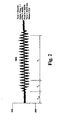
- the PR symbol has a pseudoperiodic characteristic as shown in Fig. 2 and differs in each of three transmission modes of the Eureka 147 system in accordance with the network configuration and operating frequencies.
- this pseudoperiodicity is of 128 samples or bits because of the repetitive pattern of the time-frequency-phase parameters, h 0 j, h 1 j, h 2 j, and h 3 j, that appear sequentially in the PR symbol. This is shown in the following Table: j 0 1 2 3 4 5 6 7 8 9 10 11 12 13 14 15 h 0 . .j 0 2 0 0 0 0 1 1 2 0 0 0 2 2 1 1 h 1 .
- this pseudoperiodicity is used to achieve frame, or coarse, synchronization.
- the PR symbol follows the null symbol.
- the main OFDM signal strength is approximately equal to zero or that of noise.
- T null represents the duration of the null symbol and no OFDM symbols are present during this period.
- T u represents the duration of the OFDM symbols
- T g represents the duration of a guard interval. Therefore, the PR symbol acts not only as a reference for differential quadrature phase shift key ("QPSK”) modulation and demodulation for the next OFDM symbol, but also as a pilot tone for synchronization.
- QPSK differential quadrature phase shift key
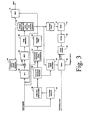
- Fig. 3 illustrates a synchronization system constructed in accordance with the present invention.
- an envelope detector 10 receives an input signal and begins detecting for the first symbol of the OFDM input signal, which is the null symbol.
- Envelope detector 10 also provides the amplitude of the input signal to a filter and differentiator 20.
- envelope detector 10 triggers filter and differentiator 20 for the detection of the second symbol, which is the PR symbol, based on the pseudoperiodicity of the PR symbol.
- random fluctuations between samples render differentiation of symbols difficult.
- fitter and differentiator 20 establishes a clear transition from the first symbol, null, to the second symbol, PR, and then a transition detection circuit 30 detects the null to PR transition.
- Fig. 4 shows a preferred embodiment of filter and differentiator circuit 20, which generates a smooth waveform and a pseudoperiodic waveform from the input signal.
- the smooth waveform is used to assure the proper detection of the null symbol.
- the pseudoperiodic waveform is used to detect the PR symbol by comparing a PR to null power ratio to a predetermined threshold value.
- the threshold value may be taken between signal and noise levels to indicate null to PR transition at the beginning of data frames.
- the signal value in a digital audio broadcasting system, varies with distance and fading environment. However, the noise level is relatively constant, e.g., thermal noise of approximately -112 dBm.
- the threshold value may be set based on the noise level. After the threshold value has been set, the OFDM symbols in the input signal are compared to the threshold value, and the numbers of samples larger and smaller than the threshold value are separately recorded. The null to PR transition is located when the number of samples having values greater than the threshold value is larger than the number of samples having values smaller than the threshold value. Once the null and PR symbols are detected, frame synchronization is achieved.
- the null to PR transition also generates a low rate frame clock used to trigger a sampling clock for fast Fourier transform ("FFT") processing of the symbols for synchronization and DPQSK demodulation.
- a frame clock generator 60 is triggered by transition detection circuit 30, which detects the null to PR transition in light of the smooth and pseudoperiodic waveforms provided by filter and differentiator 20. Transition detection circuit 30 also detects the transition time between null and PR symbols.
- Clock generator 60 having been triggered by transition detection circuit 30, provides a frame clock to a timer 62, which may be manually selected by a user. Timer 62 then provides the clock signal to a fast Fourier transform circuit 82.
- Clock generator 60 also receives a correction to the frame dock from a synchronization decision circuit 92. Additional discussion regarding the generation and correction of frame clock signals is set forth below.
- filter and differentiator circuit 20 includes a filter portion and a differentiator portion.
- the filter portion is a two-tap filter to smooth the sample to sample fluctuations and includes a one-sample delay filter 21 applied to an input signal.
- An adder 22 combines a delayed input signal with the input signal.
- the differentiator portion is connected to adder 22 and enhances the pseudoperiodicity characteristic of the second symbol by producing a pseudoperiodic waveform.
- the enhancement of the pseudoperiodicity characteristic of the second symbol of the input signal may be accomplished by three n/2 th order delay filters 23, 24, and 25, where n is equal to the number of samples in the input signal, and a 4-tap summation. This portion of filter and differentiator 20 obtains the difference between two taps and adds two successive differences to smooth the randomness of the input signal.
- the input signal is provided to a first filter, which includes one-sample delay filter 21 and adder 22.
- Transfer function H p (z) is implemented as shown in Fig. 4 through filters 23, 24, and 25, and summation circuits 27, 28, and 29.
- the circuit that implements H B (z) is represented by z-transform filters 23, 24, and 25 and a summation circuit 26.
- H p (z) (1 - z -64 + z -128 - z -192 ) to produce a pseudoperiodic waveform
- H B (z) (1 + z -64 + z -128 + z -192 ) to produce a smooth waveform.
- Each of z-transform filters 23, 24, and 25, applies a 64-sample delay to the signal applied thereto.
- summation circuit 27 subtracts the output of filter 23 from the output of adder 22.
- Summation circuit 28 subtracts the output of filter 25 from the output of filter 24.
- the multiple locations of peaks of the pseudoperiodic waveform are more accurate indicators of a reference signal frame.
- the average value of the peaks is greater than a predetermined threshold level, then the likelihood of a false detection of the PR symbol, or a false alarm, which occurs often in deep fading conditions, may be decreased. Therefore, in a preferred embodiment, the average value and mean location from a predetermined number of peaks of the pseudoperiodic waveform are obtained to more accurately determine the beginning, or end, of the PR symbol.
- the smooth and pseudoperiodic waveforms are provided to transition detection circuit 30 to ensure that the first and second symbols have been correctly located because fluctuations between samples may interfere with the ability of the envelope detector to correctly detect and distinguish the first and second symbols.
- frame synchronization, or coarse synchronization will have been achieved.
- the duration of the guard interval should be long enough to alleviate multipath distortion.
- the duration of the guard interval T g of the Eureka 147 signal is approximately 1 ⁇ 4 of the symbols' duration T u , and the symbols in the guard interval are reproduced from the final 1 ⁇ 4 of the symbols.
- the guard intervals introduced to the Eureka 147 system signals are further used to estimate a fractional frequency offset of the carrier frequency offset.
- Carrier phase synchronization or fine tuning, is required after frame synchronization to obtain complete signal synchronization.
- Conventional methods and systems attain carrier frequency synchronization by first estimating the integral frequency offset of the carrier frequency and then compensating for the fractional frequency offset.
- embodiments in accordance with the present invention first estimate fractional frequency offset and then obtain the integral frequency offset by using the estimated fractional frequency offset as a reference to avoid ambiguity in integral frequency offset estimation as may be encountered with conventional methods and systems. The relationship between guard intervals and estimation of fractional frequency offset is described below.
- the middle portion of the block diagram in Fig. 3 includes a circuit for estimating fractional frequency offset based on the introduction of the guard interval.
- An OFDM digital signal r(t) input to the synchronization system is provided to a circuit 40 for fractional frequency offset estimation.
- a more detailed block diagram of circuit 40 is shown in Fig. 6, which includes a delay circuit 72, a first arithmetic circuit 74, a multiplier circuit 76, and a second arithmetic circuit 77.
- the input signal r(t) is provided to delay circuit 72 which delays the signal by a delay period equal to that of the signal duration T u .
- Coupled to delay circuit 72 is first arithmetic circuit 74 to provide a complex conjugate r*(t- T u ) of an output of delay circuit 72. Coupled to arithmetic circuit 74 is multiplier circuit 76, which also receives the input signal r(t), to multiply the input signal with an output of arithmetic circuit 74.
- 2 e j 2 ⁇ ⁇ f ⁇ t + j 2 ⁇ ⁇ f R t ⁇ j 2 ⁇ ⁇ f I t + j 2 ⁇ ⁇ f I T u ⁇ j 2 ⁇ ⁇ f R t + j 2 ⁇ ⁇ f R T u c e j 2 ⁇ ⁇ f R T u e j 2 ⁇ ⁇ f I T u
- the fractional frequency offset is then compensated by an analog automatic frequency control ("AFC”) circuit whenever OFDM symbols occur.
- AFC analog automatic frequency control
- Both Figs. 3 and 6 show the remaining process for estimation of the fractional frequency offset.
- the output of circuit 40 of Fig. 3 is produced at the output of second arithmetic circuit 77 of Fig. 6.
- Arithmetic circuit 77 coupled to multiplier circuit 76, obtains an argument value of the output of multiplier circuit 76 and divides the argument value by a product of two multiplied by n multiplied by the predetermined delay interval, T u .
- the result is then provided to an average filter circuit 50 to determine the estimated fractional frequency offset ⁇ f R of the input signal.
- the estimated fraction frequency offset is then subjected to digital-to-analog conversion by a DAC 52 and compensated by the AFC circuit.
- the integral frequency offset may be obtained through matched filtering against PR symbols of residual integral frequency offsets, since the possible residual integral frequency offsets to be matched are limited.
- an exponential circuit 78 is applied to the estimated fractional frequency offset
- a multiplication circuit 75 multiplies the exponential value with the input signal in the frequency domain.
- the output of multiplication circuit 75 is intended to be matched against several local PR symbols offset by the corresponding integral frequency offsets.
- an FFT is applied to the output of circuit 75, the output of which is multiplied with a frequency shifted PR symbol and then subject to an inverse FFT operation. The peak of the inverse fast Fourier transformed signal is then detected.
- a FFT circuit 82 transforms an output of multiplier 75.
- An output of circuit 82 is provided to a second multiplying circuit 84, which is respectively connected to circuit 82 and a frequency shifted phase reference circuit 86 to multiply the respective outputs of circuit 82 and frequency shifted phase reference circuit 86.
- Circuit 86 receives a phase reference in the frequency domain from synchronization tracking circuit 92 shifted by an integer offset determined by circuit 92.
- the product of multiplying circuit 84 is applied to an inverse FFT circuit 88.
- a peak detection circuit 90 coupled to the output of inverse FFT circuit 88 detects occurrence of a peak to indicate the carrier frequency offset.
- Multiplier circuit 84, frequency shifted phase reference circuit 86, inverse FFT circuit 88, and peak detection circuit 90 of Fig. 6 correspond to the circuits designated by the same reference numerals in Fig. 3.
- Synchronization tracking circuit 92 also provides for frame clock correction to frame dock generator 60 as described above. Through the matched filtering process, synchronization tracking circuit detects the maximum peak amplitude of an integral frequency offset through a set of possible integral frequency offsets. The coordinate of the integral frequency offset having the maximum value is provided to frame clock generator 60. A correction to the frame clock is also provided if the coordinate of the integral frequency offset is not at zero. Referring to Fig. 3, in addition to providing an input to frame dock generator 60, synchronization tracking circuit 92 provides an input to an average filter 61 and other components that constitute a path for adjusting sampling dock rate at timer 62, if necessary.
- the sampling clock adjustment loop includes average filter 61, a DAC circuit 63, a VCXO circuit 65, a clock divider 67, and timer 62. Together with synchronization tracking circuit 92 and frame clock generator 60, the sampling clock adjustment loop comprises a path for adjusting sampling clock phase to compensate for frame, or symbol, timing offset.
- the carrier frequency offset is determined through matched filtering by using the PR symbol as a reference.
- one PR symbol will match most closely with the received input signal and will have a peak output, while the other PR symbols will generate noise-like outputs after inverse FFT.
- This result may be obtained through iteration, where the output of inverse FFT circuit 88 is matched against a PR symbol corresponding to a first integral frequency offset to obtain a first peak amplitude ("PA") and first peak position ("PP").
- PA peak amplitude
- PP peak position
- Another PR symbol corresponding to a second integral frequency offset is matched with the output of multiplication circuit 75 to obtain a second PA and second PP.
- the aforementioned iterative matched filtering process may also be performed in parallel, as shown in Fig. 7.
- a plurality of multiplication circuits 84-1, 84-2, 84-3 ... 84-N, where N is the number of multiplication circuits are provided.
- Each of the N multiplication circuits receives an input signal from FFT circuit 82 as shown in Fig. 6, and each is coupled to one of a plurality of inverse FFT circuits 88-1. 88-2, 88-3 ... 88-N.
- Each of the plurality of inverse FFT circuits is connected to one of a plurality of peak detection circuits 90-1, 90-2, 90-3 ... 90-N.
- the plurality of multiplication circuits, the plurality of inverse FFTs, and the plurality of peak detection circuits correspond to the multiplication circuit 84, inverse FFT circuit 88, and peak detection circuit 90, respectively, of Figs. 3 and 6.
- Each of the plurality of peak detection circuits detects peak amplitudes and peak positions corresponding to each possible integral frequency offset. Referring again to Fig. 7, these values are simultaneously provided to a selector 94 which determines the largest peak amplitude.
- the integral frequency offset that corresponds to the largest peak amplitude is the integral frequency offset sought.
- synchronization tracking circuit 92 as shown in Fig. 3 is included in the synchronization apparatus to compare and ascertain whether previously established synchronization has been lost. If synchronization has not been lost, the synchronization system of the present invention is able to establish synchronization in an expedited manner.
- the tracking circuit may be designed such that it not only tracks synchronization of carrier frequency offset as a whole, but also fractional and integral frequency offsets individually.
- the byproduct of frequency offset compensation is symbol/clock synchronization.
- the position of the peak, PP is the time difference (offset) between the the PR symbol and the input signal. Therefore, dock synchronization is also obtained.
Landscapes
- Engineering & Computer Science (AREA)
- Computer Networks & Wireless Communication (AREA)
- Signal Processing (AREA)
- Synchronisation In Digital Transmission Systems (AREA)
Claims (12)
- Dispositif pour la détection du décalage de porteuse et la synchronisation de l'horloge de trame conjointes dans un signal d'entrée OFDM (Orthogonal Frequency Division Multiplexing) modulé, le signal d'entrée étant structuré en trames, chaque trame ayant un premier symbole présentant une puissance de signal significativement inférieure à un second symbole, le second symbole étant un signal de référence de phase ayant une pseudo-périodicité, chaque symbole ayant un intervalle de protection suivi d'une portion de données, l'intervalle de protection reproduisant la dernière partie de la portion de données, comprenant :un moyen (10, 20, 30) destiné à recevoir ledit signal d'entrée OFDM modulé et à générer une horloge de trame en se basant sur la transition entre le premier et le second symbole ;un moyen (40, 50) destiné à recevoir ledit signal d'entrée OFDM modulé et à obtenir un décalage de fréquence de porteuse fractionnel en détectant le décalage de fréquence de la dernière partie d'un symbole par rapport à l'intervalle de protection correspondant ;un moyen (75) destiné à compenser un second symbole reçu avec ledit décalage de fréquence de porteuse fractionnel ;un moyen (82) destiné à effectuer la transformation rapide de Fourier du second symbole compensé et à générer le signal de sortie de transformée rapide de Fourier ;un moyen (84, 86) destiné à accorder ledit signal de sortie de transformée rapide de Fourier avec un signal de référence de phase qui a été décalé en utilisant un décalage de fréquence entier et en générant un signal de sortie accordé en fréquence ;un moyen (88) destiné à la transformation rapide de Fourier inverse du signal de sortie accordé en fréquence et à générer un signal de sortie accordé dans le temps ;un moyen (90, 92) destiné à recevoir ledit signal de sortie accordé dans le temps, à déterminer un décalage de fréquence entier au moyen d'un ensemble de décalages de fréquence entiers possibles en se basant sur ledit signal de sortie accordé dans le temps reçu, à fournir ledit décalage de fréquence entier déterminé audit moyen d'accord (84, 86) et à générer un signal de correction de fréquence d'horloge de trame en se basant sur le décalage de fréquence entier déterminé ; etun moyen (60) destiné à recevoir ladite horloge de trame et ledit signal de correction de fréquence d'horloge de trame et à fournir une horloge de trame synchronisée.
- Dispositif selon la revendication 1, dans lequel ledit moyen destiné à recevoir ledit signal d'entrée OFDM modulé et à générer une horloge de trame comprend un circuit de détection d'enveloppe (10) et un circuit permettant d'améliorer la pseudo-périodicité (20).
- Dispositif selon la revendication 1 ou 2, dans lequel ledit moyen destiné à recevoir ledit signal de sortie accordé dans le temps, à déterminer et à fournir un décalage de fréquence de porteuse entier comprend :un moyen de détection de crête (90) destiné à fournir une amplitude et une position du signal de crête à partir du signal de sortie accordé dans le temps,une mémoire couplée audit moyen de détection de crête (90) destinée à conserver une pluralité d'amplitudes et de positions pour une pluralité de décalages de fréquence de porteuse entiers, etun moyen (94) couplé à ladite mémoire pour comparer ladite pluralité d'amplitudes stockées dans ladite mémoire et pour déterminer celle qui présente l'amplitude la plus importante.
- Dispositif selon la revendication 3, dans lequel ledit moyen (94) couplé à ladite mémoire est en outre adapté pour déterminer le décalage de fréquence de porteuse entier en se basant sur ladite amplitude la plus importante et pour générer ledit signal de correction de fréquence d'horloge de trame en se basant sur la position de crête correspondante.
- Dispositif selon l'une quelconque des revendications 1 à 4, dans lequel ledit moyen de réception dudit signal de sortie accordé dans le temps, de détermination et de fourniture d'un décalage de fréquence entier comprend en outre un moyen de suivi (92) destiné à comparer ledit décalage de fréquence de porteuse entier avec un décalage de fréquence de référence pour déterminer si la synchronisation a été perdue.
- Dispositif selon l'une quelconque des revendications 1 à 5, dans lequel ledit moyen destiné à recevoir ledit signal de sortie OFDM modulé et à générer une horloge de trame comprend un moyen de filtrage (20) ayant une fonction de transfert Hp (Z) = (1 - z-n/2 + Z-n- Z-3n/2), dans laquelle n est un nombre d'échantillons dans le signal d'entrée, pour produire une forme d'onde pseudo-périodique.
- Dispositif selon l'une quelconque des revendications 1 à 6, dans lequel ledit signal d'entrée OFDM modulé est conforme à la norme Eureka 147.
- Procédé pour la détection du décalage de porteuse et la synchronisation de l'horloge de trame conjointes dans un signal d'entrée OFDM modulé, le signal d'entrée étant structuré en trames, chaque trame ayant un premier symbole présentant une puissance de signal significativement inférieure à un second symbole, le second symbole étant un signal de référence de phase ayant une pseudo-périodicité, chaque symbole ayant un intervalle de protection suivi d'une portion de données, l'intervalle de protection reproduisant la dernière partie de la portion de données, comprenant les étapes consistant à :recevoir ledit signal d'entrée OFDM modulé ;générer une horloge de trame en se basant sur la transition entre le premier et le second symbole ;obtenir un décalage de fréquence de porteuse fractionnel en détectant le décalage de fréquence de la dernière partie d'un symbole par rapport à l'intervalle de protection correspondant ;compenser un second symbole reçu avec ledit décalage de fréquence de porteuse fractionnel ;générer un signal de sortie de transformée de Fourier rapide par une transformation rapide de Fourier du second symbole compensé ;générer un signal de sortie accordé en fréquence en accordant ledit signal de sortie de transformée rapide de Fourier avec un signal de référence de phase, qui a été décalé en utilisant un décalage entier de fréquence ;générer un signal de sortie accordé dans le temps par une transformation rapide de Fourier inverse du signal de sortie accordé en fréquence ;déterminer un décalage de fréquence entier par un ensemble de décalages de fréquence entiers possibles en se basant sur ledit signal de sortie accordé dans le temps ;générer un signal de correction de fréquence d'horloge de trame en se basant sur le décalage de fréquence entier déterminé ; etfournir une horloge de trame synchronisée en se basant sur ladite horloge de trame et ledit signal de correction de fréquence d'horloge de trame.
- Procédé selon la revendication 8, dans lequel ladite étape consistant à générer une horloge de trame comprend les étapes de détection d'enveloppe et d'amélioration de la pseudo-périodicité.
- Procédé selon la revendication 8 ou 9, dans lequel ladite étape consistant à déterminer un décalage de fréquence de porteuse entier comprend les étapes consistant à :détecter une crête pour obtenir l'amplitude et la position d'un signal de crête, à partir du signal de sortie accordé dans le temps ;conserver, en la stockant dans une mémoire, une pluralité d'amplitudes et de positions pour la pluralité de décalages de fréquence de porteuse entiers fournis par ladite étape de détection de crête ;comparer ladite pluralité d'amplitudes stockée dans ladite mémoire, etdéterminer celle qui présente l'amplitude la plus importante.
- Procédé selon la revendication 10, dans lequel ladite amplitude la plus importante détermine le décalage de fréquence de porteuse entier et la position de crête correspondante donne ledit signal de correction de fréquence d'horloge de trame.
- Procédé selon l'une quelconque des revendications 8 à 11, comprenant en outre, après ladite étape consistant à déterminer un décalage de fréquence de porteuse entier, l'étape consistant à comparer ledit décalage de fréquence de porteuse entier avec un décalage de fréquence de référence pour déterminer si la synchronisation a été perdue.
Applications Claiming Priority (3)
| Application Number | Priority Date | Filing Date | Title |
|---|---|---|---|
| US08/872,671 US6058101A (en) | 1997-06-11 | 1997-06-11 | Synchronization method and system for a digital receiver |
| US872671 | 1997-06-11 | ||
| EP97113328A EP0884878B1 (fr) | 1997-06-11 | 1997-08-01 | Synchronisation de trame, d'horloge de symbole et de porteuse dans des récepteurs de signaux multiporteuses |
Related Parent Applications (1)
| Application Number | Title | Priority Date | Filing Date |
|---|---|---|---|
| EP97113328A Division EP0884878B1 (fr) | 1997-06-11 | 1997-08-01 | Synchronisation de trame, d'horloge de symbole et de porteuse dans des récepteurs de signaux multiporteuses |
Publications (2)
| Publication Number | Publication Date |
|---|---|
| EP1434403A1 EP1434403A1 (fr) | 2004-06-30 |
| EP1434403B1 true EP1434403B1 (fr) | 2006-10-25 |
Family
ID=25360079
Family Applications (2)
| Application Number | Title | Priority Date | Filing Date |
|---|---|---|---|
| EP04004148A Expired - Lifetime EP1434403B1 (fr) | 1997-06-11 | 1997-08-01 | Détection d'un décalage de porteuse et synchronisation d'un horloge de trame dans un récepteur de signaux multiporteurs |
| EP97113328A Expired - Lifetime EP0884878B1 (fr) | 1997-06-11 | 1997-08-01 | Synchronisation de trame, d'horloge de symbole et de porteuse dans des récepteurs de signaux multiporteuses |
Family Applications After (1)
| Application Number | Title | Priority Date | Filing Date |
|---|---|---|---|
| EP97113328A Expired - Lifetime EP0884878B1 (fr) | 1997-06-11 | 1997-08-01 | Synchronisation de trame, d'horloge de symbole et de porteuse dans des récepteurs de signaux multiporteuses |
Country Status (5)
| Country | Link |
|---|---|
| US (1) | US6058101A (fr) |
| EP (2) | EP1434403B1 (fr) |
| CA (1) | CA2208626C (fr) |
| DE (2) | DE69736866T2 (fr) |
| TW (1) | TW431098B (fr) |
Cited By (2)
| Publication number | Priority date | Publication date | Assignee | Title |
|---|---|---|---|---|
| WO2010068021A3 (fr) * | 2008-12-11 | 2010-08-19 | Lg Electronics, Inc. | Procédé d'émission et de réception de signal et appareil d'émission et de réception de signal |
| US11290314B2 (en) | 2017-08-10 | 2022-03-29 | Huawei Technologies Co., Ltd. | Transmitting device, receiving device and methods thereof |
Families Citing this family (65)
| Publication number | Priority date | Publication date | Assignee | Title |
|---|---|---|---|---|
| DE69718799T2 (de) * | 1996-09-02 | 2003-11-13 | Stmicroelectronics N.V., Amsterdam | Verbesserungen in, oder in bezug auf mehrträgerübertragungssysteme |
| DE19653261A1 (de) * | 1996-12-20 | 1998-06-25 | Alsthom Cge Alcatel | Synchrones digitales Nachrichtenübertragungssystem, Steuerungseinrichtung, Netzelement und zentraler Taktgenerator |
| KR100238047B1 (ko) * | 1997-02-25 | 2000-01-15 | 윤종용 | 직교 주파수분할 다중화 전송시스템의 반송파 주파수 동기 방법 및 동기 장치 |
| JP3568180B2 (ja) * | 1997-06-12 | 2004-09-22 | 株式会社日立国際電気 | データ伝送装置 |
| EP0895387A1 (fr) * | 1997-07-28 | 1999-02-03 | Deutsche Thomson-Brandt Gmbh | Détection du mode de transmission d'un signal vidéo numérique télédiffusé |
| JPH1155212A (ja) * | 1997-07-31 | 1999-02-26 | Sony Corp | ディジタル情報信号受信装置 |
| US6253347B1 (en) * | 1997-11-05 | 2001-06-26 | Hitachi America, Ltd. | Automatic synchronization circuit for trellis decoder |
| EP0929172B1 (fr) * | 1998-01-06 | 2010-06-02 | MOSAID Technologies Inc. | Système de modulation multiporteuse, à débits de symboles variables |
| US6876675B1 (en) * | 1998-02-06 | 2005-04-05 | Cisco Technology, Inc. | Synchronization in OFDM systems |
| JPH11252038A (ja) * | 1998-02-27 | 1999-09-17 | Sony Corp | デジタル放送の受信機 |
| WO1999053666A1 (fr) * | 1998-04-14 | 1999-10-21 | Fraunhofer-Gesellschaft zur Förderung der angewandten Forschung e.V. | Structure de trames et synchronisation de trames pour des systemes a porteuses multiples |
| US6259893B1 (en) * | 1998-11-03 | 2001-07-10 | Ibiquity Digital Corporation | Method and apparatus for reduction of FM interference for FM in-band on-channel digital audio broadcasting system |
| FR2788907B1 (fr) * | 1999-01-27 | 2001-04-13 | St Microelectronics Sa | Generation d'intervalle de garde dans une transmission en modulation dmt |
| US6074086A (en) * | 1999-04-26 | 2000-06-13 | Intellon Corporation | Synchronization of OFDM signals with improved windowing |
| US6891792B1 (en) * | 1999-05-14 | 2005-05-10 | At&T Corp. | Method for estimating time and frequency offset in an OFDM system |
| JP3675670B2 (ja) * | 1999-05-27 | 2005-07-27 | パイオニア株式会社 | 受信装置 |
| ATE340465T1 (de) * | 1999-06-16 | 2006-10-15 | Sony Deutschland Gmbh | Optimierte synchronisierungspräambelstruktur für ofdm-system |
| US6807147B1 (en) | 1999-06-23 | 2004-10-19 | At&T Wireless Services, Inc. | Methods and apparatus for use in obtaining frame synchronization in an OFDM communication system |
| KR100362571B1 (ko) * | 1999-07-05 | 2002-11-27 | 삼성전자 주식회사 | 직교주파수분할다중 시스템에서 파일럿 심볼을 이용한 주파수 오류 보상장치 및 방법 |
| JP3190318B2 (ja) * | 1999-07-07 | 2001-07-23 | 三菱電機株式会社 | 周波数誤差推定装置および周波数誤差推定方法 |
| US6810074B1 (en) * | 1999-09-06 | 2004-10-26 | Samsung Electronics Co., Ltd. | Apparatus and method for detecting a received on-off keying signal in a CDMA mobile communication system |
| DE10039902B4 (de) * | 2000-08-16 | 2011-04-28 | Rohde & Schwarz Gmbh & Co. Kg | Verfahren zur Frequenz- und Zeit-Synchronisation eines Empfängers |
| NZ506558A (en) * | 2000-08-25 | 2003-04-29 | Ind Res Ltd | A broadband indoor communication system using ofdm |
| US6560303B1 (en) * | 2000-10-26 | 2003-05-06 | Comsat Corporation | Joint frame, carrier and clock synchronization scheme |
| CN1141815C (zh) * | 2000-12-18 | 2004-03-10 | 信息产业部电信传输研究所 | 一种码分多址多径衰落信道的频率自动校正装置 |
| US7012881B2 (en) * | 2000-12-29 | 2006-03-14 | Samsung Electronic Co., Ltd. | Timing and frequency offset estimation scheme for OFDM systems by using an analytic tone |
| NZ509688A (en) * | 2001-02-01 | 2003-06-30 | Ind Res Ltd | Maximum likelihood sychronisation (estimating time delay) for wireless digital communications system using a pilot symbol |
| US6473420B1 (en) * | 2001-02-16 | 2002-10-29 | Harris Corporation | Wideband ranging process for frequency acquisition |
| US8619922B1 (en) | 2002-02-04 | 2013-12-31 | Marvell International Ltd. | Method and apparatus for acquisition and tracking of orthogonal frequency division multiplexing symbol timing, carrier frequency offset and phase noise |
| US7218691B1 (en) | 2001-03-05 | 2007-05-15 | Marvell International Ltd. | Method and apparatus for estimation of orthogonal frequency division multiplexing symbol timing and carrier frequency offset |
| DE10112773B4 (de) * | 2001-03-16 | 2012-09-20 | Rohde & Schwarz Gmbh & Co Kg | Verfahren zur Frequenz- und Zeit-Synchronisation eines OFDM-Empfängers |
| KR20020082642A (ko) * | 2001-04-25 | 2002-10-31 | 주식회사 호서텔넷 | 리프렉스(ReFLEX) 전송방식에서의 프레임동기검출장치 및 그 방법 |
| US6868130B2 (en) * | 2001-04-25 | 2005-03-15 | Silicon Integrated Systems Corp. | Transmission mode detector for digital receiver |
| US6959050B2 (en) * | 2001-06-15 | 2005-10-25 | Motorola, Inc. | Method and apparatus for synchronizing an OFDM signal |
| US7035364B2 (en) * | 2001-06-29 | 2006-04-25 | Motorola, Inc. | Digital receiver fast frequency and time acquisition system using a single synchronization word and method of using same |
| US6985531B2 (en) * | 2001-07-13 | 2006-01-10 | Cyntrust Communications, Inc. | Dual domain differential encoder/decoder |
| KR100807886B1 (ko) * | 2001-09-24 | 2008-02-27 | 에스케이 텔레콤주식회사 | 직교 주파수 분할 다중화 시스템의 수신 장치 |
| US7065171B1 (en) * | 2001-10-22 | 2006-06-20 | Cingular Wireless Ii, Llc | Method for synchronization of received signals |
| KR100790114B1 (ko) * | 2002-03-16 | 2007-12-31 | 삼성전자주식회사 | 직교주파수 분할다중 접속 시스템에서 적응적 파일럿반송파 할당 방법 및 장치 |
| US8094591B1 (en) * | 2002-03-19 | 2012-01-10 | Good Technology, Inc. | Data carrier detector for a packet-switched communication network |
| KR100553544B1 (ko) * | 2002-08-31 | 2006-02-20 | 삼성탈레스 주식회사 | 버스트 직교 주파수분할 다중 전송 시스템에서 주파수 오프셋 추정 및 채널 등화방법 |
| KR100492359B1 (ko) * | 2002-09-18 | 2005-05-31 | 한기열 | 오에프디엠 시스템의 심볼동기 검출장치 |
| ES2212744B2 (es) | 2003-01-10 | 2005-03-16 | Diseño De Sistemas En Silicio, S.A. | Procedimiento de sincronizacion en el dominio del tiempo y de la frecuencia de multiples equipos en un sistema de transmision con modulacion ofdm. |
| JP4338532B2 (ja) * | 2003-02-21 | 2009-10-07 | 富士通株式会社 | 通信装置 |
| US7277457B2 (en) * | 2003-10-03 | 2007-10-02 | Motorola, Inc. | Sync bursts for frequency offset compensation |
| KR100587310B1 (ko) | 2004-08-18 | 2006-06-08 | 엘지전자 주식회사 | 주파수 동기 장치 및 이를 적용한 dvb-h 수신 시스템 |
| KR100720546B1 (ko) * | 2004-12-17 | 2007-05-22 | 엘지전자 주식회사 | 디지털 수신기의 동기 포착 장치 및 방법 |
| WO2007147107A2 (fr) | 2006-06-16 | 2007-12-21 | Qualcomm Incorporated | Codage d'informations dans des signaux de balise |
| US7876863B2 (en) * | 2006-08-10 | 2011-01-25 | Cisco Technology, Inc. | Method and system for improving timing position estimation in wireless communications networks |
| KR100770898B1 (ko) * | 2006-09-29 | 2007-10-26 | 삼성전자주식회사 | 무선통신시스템에서 잡음 측정장치 및 방법 |
| KR101405965B1 (ko) * | 2007-06-25 | 2014-06-12 | 엘지전자 주식회사 | 디지털 방송 시스템 및 데이터 처리 방법 |
| KR101339424B1 (ko) | 2007-07-16 | 2013-12-09 | 삼성전자주식회사 | 샘플링 주파수 오프셋 추정 방법, 샘플링 주파수 오프셋추정 장치 및 그 장치를 구비하는 샘플링 타이밍 복원 루프 |
| US20090135799A1 (en) * | 2007-11-27 | 2009-05-28 | Harris Corporation | Wireless communications device including path searcher with common coherent correlator and related methods |
| US7961816B2 (en) * | 2007-11-28 | 2011-06-14 | Industrial Technology Research Institute | Device for and method of signal synchronization in a communication system |
| KR101016946B1 (ko) * | 2008-12-16 | 2011-02-28 | 한국과학기술원 | T―dmb 수신 장치 및 그 동작 방법 |
| JP5515718B2 (ja) * | 2009-12-17 | 2014-06-11 | 株式会社Jvcケンウッド | 無線通信装置及び無線通信方法 |
| TWI394026B (zh) * | 2010-01-07 | 2013-04-21 | 立錡科技股份有限公司 | 時脈產生器以及應用該時脈產生器的相位交錯時脈同步裝置及方法 |
| CN102611907B (zh) * | 2012-03-16 | 2014-04-09 | 清华大学 | 一种多分辨率视频原地滤波方法及其装置 |
| CN103458495A (zh) * | 2012-05-30 | 2013-12-18 | 富士通株式会社 | 一种载波聚合系统中的信号同步方法和装置 |
| DE102012217871A1 (de) * | 2012-09-28 | 2014-04-03 | Behr Gmbh & Co. Kg | Wärmeübertrager |
| US9237002B2 (en) | 2014-01-30 | 2016-01-12 | Imagine Communications Corp. | Null-gating signal detection |
| US9647719B2 (en) * | 2015-02-16 | 2017-05-09 | Federated Wireless, Inc. | Method, system, and apparatus for spectrum sensing of radar signals |
| KR101811221B1 (ko) * | 2016-02-17 | 2017-12-21 | 주식회사 이노와이어리스 | 신호 분석기의 wcdma 신호 타이밍 오프셋 처리 방법 |
| CN114915316B (zh) * | 2022-03-31 | 2023-03-24 | 中国人民解放军战略支援部队航天工程大学 | 一种基于频域处理的带限直扩信号数字码跟踪方法 |
| US11737044B1 (en) | 2022-12-12 | 2023-08-22 | Ultralogic 6G, Llc | Mid-symbol timestamp point for precision synchronization in 5G and 6G |
Family Cites Families (14)
| Publication number | Priority date | Publication date | Assignee | Title |
|---|---|---|---|---|
| JPS5853352B2 (ja) * | 1979-10-03 | 1983-11-29 | 日本電信電話株式会社 | 音声合成器 |
| FR2670062B1 (fr) * | 1990-11-30 | 1993-11-12 | Thomson Csf | Procede de recalage des oscillateurs locaux d'un recepteur et dispositif pour la mise en óoeuvre du procede. |
| US5170413A (en) * | 1990-12-24 | 1992-12-08 | Motorola, Inc. | Control strategy for reuse system assignments and handoff |
| SG44771A1 (en) * | 1991-02-28 | 1997-12-19 | Philips Electronics Nv | System for broadcasting and receiving digital data receiver and transmitter for use in such system |
| US5402334A (en) * | 1992-05-11 | 1995-03-28 | The United States Of America As Represented By The Secretary Of The Navy | Method and apparatus for pseudoperiodic drive |
| US5323391A (en) * | 1992-10-26 | 1994-06-21 | Motorola, Inc. | Multi-channel digital transmitter and receiver |
| US5479363A (en) * | 1993-04-30 | 1995-12-26 | The Regents Of The University Of California | Programmable digital signal processor using switchable unit-delays for optimal hardware allocation |
| US5444697A (en) * | 1993-08-11 | 1995-08-22 | The University Of British Columbia | Method and apparatus for frame synchronization in mobile OFDM data communication |
| DE69428526D1 (de) * | 1994-06-30 | 2001-11-08 | St Microelectronics Srl | Filterverfahren und digitales Überabtastungsfilter mit endlicher Impulsantwort und mit vereinfachter Steuereinheit |
| GB2340003B (en) * | 1994-12-15 | 2000-03-22 | Inmarsat Ltd | Multiplex communication |
| JP3130752B2 (ja) * | 1995-02-24 | 2001-01-31 | 株式会社東芝 | Ofdm伝送受信方式及び送受信装置 |
| SE514986C2 (sv) * | 1995-03-01 | 2001-05-28 | Telia Ab | Metod och anordning för synkronisering vid OFDM-system |
| GB2307155B (en) * | 1995-11-02 | 1999-09-15 | British Broadcasting Corp | Synchronisation of OFDM signals |
| US5751777A (en) * | 1996-05-03 | 1998-05-12 | Symmetricom, Inc. | Multiple input frequency locked loop |
-
1997
- 1997-06-11 US US08/872,671 patent/US6058101A/en not_active Expired - Lifetime
- 1997-06-23 CA CA002208626A patent/CA2208626C/fr not_active Expired - Lifetime
- 1997-08-01 EP EP04004148A patent/EP1434403B1/fr not_active Expired - Lifetime
- 1997-08-01 DE DE69736866T patent/DE69736866T2/de not_active Expired - Lifetime
- 1997-08-01 EP EP97113328A patent/EP0884878B1/fr not_active Expired - Lifetime
- 1997-08-01 DE DE69727792T patent/DE69727792T2/de not_active Expired - Lifetime
-
1998
- 1998-04-28 TW TW087106485A patent/TW431098B/zh not_active IP Right Cessation
Cited By (2)
| Publication number | Priority date | Publication date | Assignee | Title |
|---|---|---|---|---|
| WO2010068021A3 (fr) * | 2008-12-11 | 2010-08-19 | Lg Electronics, Inc. | Procédé d'émission et de réception de signal et appareil d'émission et de réception de signal |
| US11290314B2 (en) | 2017-08-10 | 2022-03-29 | Huawei Technologies Co., Ltd. | Transmitting device, receiving device and methods thereof |
Also Published As
| Publication number | Publication date |
|---|---|
| DE69727792T2 (de) | 2004-08-05 |
| DE69727792D1 (de) | 2004-04-01 |
| CA2208626C (fr) | 2002-03-05 |
| EP0884878A2 (fr) | 1998-12-16 |
| DE69736866T2 (de) | 2007-03-01 |
| DE69736866D1 (de) | 2006-12-07 |
| EP0884878A3 (fr) | 2002-01-09 |
| TW431098B (en) | 2001-04-21 |
| EP0884878B1 (fr) | 2004-02-25 |
| CA2208626A1 (fr) | 1998-12-11 |
| EP1434403A1 (fr) | 2004-06-30 |
| US6058101A (en) | 2000-05-02 |
Similar Documents
| Publication | Publication Date | Title |
|---|---|---|
| EP0884878B1 (fr) | Synchronisation de trame, d'horloge de symbole et de porteuse dans des récepteurs de signaux multiporteuses | |
| EP0896457B1 (fr) | Synchronisation de symbole pour signaux multiporteurs à intervalle de garde | |
| US5732113A (en) | Timing and frequency synchronization of OFDM signals | |
| EP0706273B1 (fr) | Procédé et dispositif de démodulation d'un signal transmis sur plusieurs porteuses | |
| US6711221B1 (en) | Sampling offset correction in an orthogonal frequency division multiplexing system | |
| EP1133841B1 (fr) | Systeme et procede de correction d'erreurs de synchronisation par utilisation de symboles pilotes dans un systeme de communication ofdm/cdma | |
| JP3485117B2 (ja) | Ofdm方式の基準信号の伝送方法 | |
| US6546055B1 (en) | Carrier offset determination for RF signals having a cyclic prefix | |
| US7009931B2 (en) | Synchronization in a multiple-input/multiple-output (MIMO) orthogonal frequency division multiplexing (OFDM) system for wireless applications | |
| US5802117A (en) | Method and apparatus for joint frequency offset and timing estimation of a multicarrier modulation system | |
| EP0847643B1 (fr) | Procede de simplification de la demodulation dans des systemes a emetteurs multiporteuse | |
| JP4721530B2 (ja) | 直交周波数分割多重化システムにおける局部発振器の周波数を補正する方法およびofdm受信器 | |
| US5790784A (en) | Network for time synchronizing a digital information processing system with received digital information | |
| EP1245104B1 (fr) | Correction d'un decalage de frequence d'echantillonnage dans un systeme de multiplexage par division de frequence orthogonale | |
| JP3350161B2 (ja) | 伝送システムと伝送システム用受信器 | |
| US6768714B1 (en) | Methods and apparatus for use in obtaining frequency synchronization in an OFDM communication system | |
| US5687165A (en) | Transmission system and receiver for orthogonal frequency-division multiplexing signals, having a frequency-synchronization circuit | |
| US20020065047A1 (en) | Synchronization, channel estimation and pilot tone tracking system | |
| JP3022854B1 (ja) | 遅延プロファイル解析装置及びシンボル同期方法 | |
| US10382241B2 (en) | Reception of signaling data in frequency division multiplexed broadcast system | |
| EP0901260A2 (fr) | Synchronisation de trames et de symbÔles dans des récepteurs multiporteurs | |
| US6700866B1 (en) | Methods and apparatus for use in obtaining frequency synchronization in an OFDM communication system | |
| WO1996002990A2 (fr) | Procede et dispositif de synchronisation d'un emetteur et d'un recepteur dans un systeme numerique | |
| US6574283B1 (en) | Communication method, transmission and reception apparatuses, and cellular radio communication system | |
| JP4154570B2 (ja) | 復調された受信信号から複素数データサンプルを生成する受信機において同調周波数オフセットを決定する方法および無線lan受信機 |
Legal Events
| Date | Code | Title | Description |
|---|---|---|---|
| PUAI | Public reference made under article 153(3) epc to a published international application that has entered the european phase |
Free format text: ORIGINAL CODE: 0009012 |
|
| 17P | Request for examination filed |
Effective date: 20040224 |
|
| AC | Divisional application: reference to earlier application |
Ref document number: 0884878 Country of ref document: EP Kind code of ref document: P |
|
| AK | Designated contracting states |
Kind code of ref document: A1 Designated state(s): DE FR GB NL |
|
| AKX | Designation fees paid |
Designated state(s): DE FR GB NL |
|
| 17Q | First examination report despatched |
Effective date: 20050304 |
|
| GRAP | Despatch of communication of intention to grant a patent |
Free format text: ORIGINAL CODE: EPIDOSNIGR1 |
|
| RTI1 | Title (correction) |
Free format text: CARRIER OFFSET DETECTION AND FRAME CLOCK SYNCHRONISATION IN A MULTICARRIER RECEIVER |
|
| GRAS | Grant fee paid |
Free format text: ORIGINAL CODE: EPIDOSNIGR3 |
|
| GRAA | (expected) grant |
Free format text: ORIGINAL CODE: 0009210 |
|
| AC | Divisional application: reference to earlier application |
Ref document number: 0884878 Country of ref document: EP Kind code of ref document: P |
|
| AK | Designated contracting states |
Kind code of ref document: B1 Designated state(s): DE FR GB NL |
|
| REG | Reference to a national code |
Ref country code: GB Ref legal event code: FG4D |
|
| REF | Corresponds to: |
Ref document number: 69736866 Country of ref document: DE Date of ref document: 20061207 Kind code of ref document: P |
|
| ET | Fr: translation filed | ||
| PLBE | No opposition filed within time limit |
Free format text: ORIGINAL CODE: 0009261 |
|
| STAA | Information on the status of an ep patent application or granted ep patent |
Free format text: STATUS: NO OPPOSITION FILED WITHIN TIME LIMIT |
|
| 26N | No opposition filed |
Effective date: 20070726 |
|
| REG | Reference to a national code |
Ref country code: FR Ref legal event code: PLFP Year of fee payment: 20 |
|
| PGFP | Annual fee paid to national office [announced via postgrant information from national office to epo] |
Ref country code: NL Payment date: 20160826 Year of fee payment: 20 |
|
| PGFP | Annual fee paid to national office [announced via postgrant information from national office to epo] |
Ref country code: DE Payment date: 20160826 Year of fee payment: 20 Ref country code: GB Payment date: 20160830 Year of fee payment: 20 |
|
| PGFP | Annual fee paid to national office [announced via postgrant information from national office to epo] |
Ref country code: FR Payment date: 20160825 Year of fee payment: 20 |
|
| REG | Reference to a national code |
Ref country code: DE Ref legal event code: R071 Ref document number: 69736866 Country of ref document: DE |
|
| REG | Reference to a national code |
Ref country code: NL Ref legal event code: MK Effective date: 20170731 |
|
| REG | Reference to a national code |
Ref country code: GB Ref legal event code: PE20 Expiry date: 20170731 |
|
| PG25 | Lapsed in a contracting state [announced via postgrant information from national office to epo] |
Ref country code: GB Free format text: LAPSE BECAUSE OF EXPIRATION OF PROTECTION Effective date: 20170731 |