EP1434473A2 - Technique de réduction du nombre de couches dans un dispositif d'acheminement de signaux - Google Patents
Technique de réduction du nombre de couches dans un dispositif d'acheminement de signaux Download PDFInfo
- Publication number
- EP1434473A2 EP1434473A2 EP03394085A EP03394085A EP1434473A2 EP 1434473 A2 EP1434473 A2 EP 1434473A2 EP 03394085 A EP03394085 A EP 03394085A EP 03394085 A EP03394085 A EP 03394085A EP 1434473 A2 EP1434473 A2 EP 1434473A2
- Authority
- EP
- European Patent Office
- Prior art keywords
- electrically conductive
- routing device
- conductive contact
- signal routing
- vias
- Prior art date
- Legal status (The legal status is an assumption and is not a legal conclusion. Google has not performed a legal analysis and makes no representation as to the accuracy of the status listed.)
- Withdrawn
Links
- 238000000034 method Methods 0.000 title claims abstract description 62
- 230000013011 mating Effects 0.000 claims description 22
- 229910003460 diamond Inorganic materials 0.000 claims description 5
- 239000010432 diamond Substances 0.000 claims description 5
- 230000002093 peripheral effect Effects 0.000 claims description 5
- 238000012360 testing method Methods 0.000 description 26
- 230000002411 adverse Effects 0.000 description 5
- 230000003071 parasitic effect Effects 0.000 description 4
- 238000012986 modification Methods 0.000 description 3
- 230000004048 modification Effects 0.000 description 3
- 238000012545 processing Methods 0.000 description 3
- 230000001902 propagating effect Effects 0.000 description 3
- 230000009286 beneficial effect Effects 0.000 description 2
- 230000015572 biosynthetic process Effects 0.000 description 2
- 238000013461 design Methods 0.000 description 2
- 238000011161 development Methods 0.000 description 1
- 230000000694 effects Effects 0.000 description 1
- 230000002708 enhancing effect Effects 0.000 description 1
- 230000003287 optical effect Effects 0.000 description 1
- 238000004806 packaging method and process Methods 0.000 description 1
Images








Classifications
-
- H—ELECTRICITY
- H05—ELECTRIC TECHNIQUES NOT OTHERWISE PROVIDED FOR
- H05K—PRINTED CIRCUITS; CASINGS OR CONSTRUCTIONAL DETAILS OF ELECTRIC APPARATUS; MANUFACTURE OF ASSEMBLAGES OF ELECTRICAL COMPONENTS
- H05K3/00—Apparatus or processes for manufacturing printed circuits
- H05K3/46—Manufacturing multilayer circuits
-
- H—ELECTRICITY
- H05—ELECTRIC TECHNIQUES NOT OTHERWISE PROVIDED FOR
- H05K—PRINTED CIRCUITS; CASINGS OR CONSTRUCTIONAL DETAILS OF ELECTRIC APPARATUS; MANUFACTURE OF ASSEMBLAGES OF ELECTRICAL COMPONENTS
- H05K1/00—Printed circuits
- H05K1/02—Details
- H05K1/11—Printed elements for providing electric connections to or between printed circuits
- H05K1/115—Via connections; Lands around holes or via connections
-
- H—ELECTRICITY
- H05—ELECTRIC TECHNIQUES NOT OTHERWISE PROVIDED FOR
- H05K—PRINTED CIRCUITS; CASINGS OR CONSTRUCTIONAL DETAILS OF ELECTRIC APPARATUS; MANUFACTURE OF ASSEMBLAGES OF ELECTRICAL COMPONENTS
- H05K1/00—Printed circuits
- H05K1/02—Details
- H05K1/11—Printed elements for providing electric connections to or between printed circuits
- H05K1/111—Pads for surface mounting, e.g. lay-out
- H05K1/112—Pads for surface mounting, e.g. lay-out directly combined with via connections
-
- H—ELECTRICITY
- H05—ELECTRIC TECHNIQUES NOT OTHERWISE PROVIDED FOR
- H05K—PRINTED CIRCUITS; CASINGS OR CONSTRUCTIONAL DETAILS OF ELECTRIC APPARATUS; MANUFACTURE OF ASSEMBLAGES OF ELECTRICAL COMPONENTS
- H05K1/00—Printed circuits
- H05K1/02—Details
- H05K1/0296—Conductive pattern lay-out details not covered by sub groups H05K1/02 - H05K1/0295
- H05K1/0298—Multilayer circuits
-
- H—ELECTRICITY
- H05—ELECTRIC TECHNIQUES NOT OTHERWISE PROVIDED FOR
- H05K—PRINTED CIRCUITS; CASINGS OR CONSTRUCTIONAL DETAILS OF ELECTRIC APPARATUS; MANUFACTURE OF ASSEMBLAGES OF ELECTRICAL COMPONENTS
- H05K2201/00—Indexing scheme relating to printed circuits covered by H05K1/00
- H05K2201/09—Shape and layout
- H05K2201/09209—Shape and layout details of conductors
- H05K2201/09218—Conductive traces
- H05K2201/09227—Layout details of a plurality of traces, e.g. escape layout for Ball Grid Array [BGA] mounting
-
- H—ELECTRICITY
- H05—ELECTRIC TECHNIQUES NOT OTHERWISE PROVIDED FOR
- H05K—PRINTED CIRCUITS; CASINGS OR CONSTRUCTIONAL DETAILS OF ELECTRIC APPARATUS; MANUFACTURE OF ASSEMBLAGES OF ELECTRICAL COMPONENTS
- H05K2201/00—Indexing scheme relating to printed circuits covered by H05K1/00
- H05K2201/09—Shape and layout
- H05K2201/09209—Shape and layout details of conductors
- H05K2201/095—Conductive through-holes or vias
- H05K2201/09509—Blind vias, i.e. vias having one side closed
-
- H—ELECTRICITY
- H05—ELECTRIC TECHNIQUES NOT OTHERWISE PROVIDED FOR
- H05K—PRINTED CIRCUITS; CASINGS OR CONSTRUCTIONAL DETAILS OF ELECTRIC APPARATUS; MANUFACTURE OF ASSEMBLAGES OF ELECTRICAL COMPONENTS
- H05K2201/00—Indexing scheme relating to printed circuits covered by H05K1/00
- H05K2201/09—Shape and layout
- H05K2201/09209—Shape and layout details of conductors
- H05K2201/095—Conductive through-holes or vias
- H05K2201/09536—Buried plated through-holes, i.e. plated through-holes formed in a core before lamination
-
- H—ELECTRICITY
- H05—ELECTRIC TECHNIQUES NOT OTHERWISE PROVIDED FOR
- H05K—PRINTED CIRCUITS; CASINGS OR CONSTRUCTIONAL DETAILS OF ELECTRIC APPARATUS; MANUFACTURE OF ASSEMBLAGES OF ELECTRICAL COMPONENTS
- H05K2201/00—Indexing scheme relating to printed circuits covered by H05K1/00
- H05K2201/09—Shape and layout
- H05K2201/09209—Shape and layout details of conductors
- H05K2201/095—Conductive through-holes or vias
- H05K2201/09627—Special connections between adjacent vias, not for grounding vias
-
- H—ELECTRICITY
- H05—ELECTRIC TECHNIQUES NOT OTHERWISE PROVIDED FOR
- H05K—PRINTED CIRCUITS; CASINGS OR CONSTRUCTIONAL DETAILS OF ELECTRIC APPARATUS; MANUFACTURE OF ASSEMBLAGES OF ELECTRICAL COMPONENTS
- H05K2201/00—Indexing scheme relating to printed circuits covered by H05K1/00
- H05K2201/10—Details of components or other objects attached to or integrated in a printed circuit board
- H05K2201/10613—Details of electrical connections of non-printed components, e.g. special leads
- H05K2201/10621—Components characterised by their electrical contacts
- H05K2201/10734—Ball grid array [BGA]; Bump grid array
-
- H—ELECTRICITY
- H05—ELECTRIC TECHNIQUES NOT OTHERWISE PROVIDED FOR
- H05K—PRINTED CIRCUITS; CASINGS OR CONSTRUCTIONAL DETAILS OF ELECTRIC APPARATUS; MANUFACTURE OF ASSEMBLAGES OF ELECTRICAL COMPONENTS
- H05K3/00—Apparatus or processes for manufacturing printed circuits
- H05K3/0005—Apparatus or processes for manufacturing printed circuits for designing circuits by computer
-
- H—ELECTRICITY
- H05—ELECTRIC TECHNIQUES NOT OTHERWISE PROVIDED FOR
- H05K—PRINTED CIRCUITS; CASINGS OR CONSTRUCTIONAL DETAILS OF ELECTRIC APPARATUS; MANUFACTURE OF ASSEMBLAGES OF ELECTRICAL COMPONENTS
- H05K3/00—Apparatus or processes for manufacturing printed circuits
- H05K3/40—Forming printed elements for providing electric connections to or between printed circuits
- H05K3/42—Plated through-holes or plated via connections
- H05K3/429—Plated through-holes specially for multilayer circuits, e.g. having connections to inner circuit layers
-
- H—ELECTRICITY
- H05—ELECTRIC TECHNIQUES NOT OTHERWISE PROVIDED FOR
- H05K—PRINTED CIRCUITS; CASINGS OR CONSTRUCTIONAL DETAILS OF ELECTRIC APPARATUS; MANUFACTURE OF ASSEMBLAGES OF ELECTRICAL COMPONENTS
- H05K3/00—Apparatus or processes for manufacturing printed circuits
- H05K3/46—Manufacturing multilayer circuits
- H05K3/4602—Manufacturing multilayer circuits characterized by a special circuit board as base or central core whereon additional circuit layers are built or additional circuit boards are laminated
-
- Y—GENERAL TAGGING OF NEW TECHNOLOGICAL DEVELOPMENTS; GENERAL TAGGING OF CROSS-SECTIONAL TECHNOLOGIES SPANNING OVER SEVERAL SECTIONS OF THE IPC; TECHNICAL SUBJECTS COVERED BY FORMER USPC CROSS-REFERENCE ART COLLECTIONS [XRACs] AND DIGESTS
- Y10—TECHNICAL SUBJECTS COVERED BY FORMER USPC
- Y10T—TECHNICAL SUBJECTS COVERED BY FORMER US CLASSIFICATION
- Y10T29/00—Metal working
- Y10T29/49—Method of mechanical manufacture
- Y10T29/49002—Electrical device making
- Y10T29/49004—Electrical device making including measuring or testing of device or component part
-
- Y—GENERAL TAGGING OF NEW TECHNOLOGICAL DEVELOPMENTS; GENERAL TAGGING OF CROSS-SECTIONAL TECHNOLOGIES SPANNING OVER SEVERAL SECTIONS OF THE IPC; TECHNICAL SUBJECTS COVERED BY FORMER USPC CROSS-REFERENCE ART COLLECTIONS [XRACs] AND DIGESTS
- Y10—TECHNICAL SUBJECTS COVERED BY FORMER USPC
- Y10T—TECHNICAL SUBJECTS COVERED BY FORMER US CLASSIFICATION
- Y10T29/00—Metal working
- Y10T29/49—Method of mechanical manufacture
- Y10T29/49002—Electrical device making
- Y10T29/49117—Conductor or circuit manufacturing
- Y10T29/49124—On flat or curved insulated base, e.g., printed circuit, etc.
- Y10T29/49126—Assembling bases
-
- Y—GENERAL TAGGING OF NEW TECHNOLOGICAL DEVELOPMENTS; GENERAL TAGGING OF CROSS-SECTIONAL TECHNOLOGIES SPANNING OVER SEVERAL SECTIONS OF THE IPC; TECHNICAL SUBJECTS COVERED BY FORMER USPC CROSS-REFERENCE ART COLLECTIONS [XRACs] AND DIGESTS
- Y10—TECHNICAL SUBJECTS COVERED BY FORMER USPC
- Y10T—TECHNICAL SUBJECTS COVERED BY FORMER US CLASSIFICATION
- Y10T29/00—Metal working
- Y10T29/49—Method of mechanical manufacture
- Y10T29/49002—Electrical device making
- Y10T29/49117—Conductor or circuit manufacturing
- Y10T29/49124—On flat or curved insulated base, e.g., printed circuit, etc.
- Y10T29/49128—Assembling formed circuit to base
-
- Y—GENERAL TAGGING OF NEW TECHNOLOGICAL DEVELOPMENTS; GENERAL TAGGING OF CROSS-SECTIONAL TECHNOLOGIES SPANNING OVER SEVERAL SECTIONS OF THE IPC; TECHNICAL SUBJECTS COVERED BY FORMER USPC CROSS-REFERENCE ART COLLECTIONS [XRACs] AND DIGESTS
- Y10—TECHNICAL SUBJECTS COVERED BY FORMER USPC
- Y10T—TECHNICAL SUBJECTS COVERED BY FORMER US CLASSIFICATION
- Y10T29/00—Metal working
- Y10T29/49—Method of mechanical manufacture
- Y10T29/49002—Electrical device making
- Y10T29/49117—Conductor or circuit manufacturing
- Y10T29/49124—On flat or curved insulated base, e.g., printed circuit, etc.
- Y10T29/49155—Manufacturing circuit on or in base
-
- Y—GENERAL TAGGING OF NEW TECHNOLOGICAL DEVELOPMENTS; GENERAL TAGGING OF CROSS-SECTIONAL TECHNOLOGIES SPANNING OVER SEVERAL SECTIONS OF THE IPC; TECHNICAL SUBJECTS COVERED BY FORMER USPC CROSS-REFERENCE ART COLLECTIONS [XRACs] AND DIGESTS
- Y10—TECHNICAL SUBJECTS COVERED BY FORMER USPC
- Y10T—TECHNICAL SUBJECTS COVERED BY FORMER US CLASSIFICATION
- Y10T29/00—Metal working
- Y10T29/49—Method of mechanical manufacture
- Y10T29/49002—Electrical device making
- Y10T29/49117—Conductor or circuit manufacturing
- Y10T29/49124—On flat or curved insulated base, e.g., printed circuit, etc.
- Y10T29/49155—Manufacturing circuit on or in base
- Y10T29/49165—Manufacturing circuit on or in base by forming conductive walled aperture in base
Definitions
- the present invention relates generally to multilayer signal routing devices and, more particularly, to a technique for reducing the number of layers in a signal routing device.
- the making of electrical connections between electronic components has long been accomplished using printed circuit boards.
- the first such circuit boards had only a single signal layer on a top surface thereof for routing electrical signals between electronic components mounted thereon.
- These single signal layer circuit boards have severe limitations with regard to the number of electrical signals that can be routed between electronic components mounted on the same circuit board. That is, the number of electrical signals that can be routed between electronic components mounted on a single signal layer circuit board is limited by the amount of area on the single signal layer.
- multilayer printed circuit boards may be either single or double-sided and may have multiple signal layers on the surface of and buried within the multilayer printed circuit boards.
- multilayer printed circuit boards have allowed a large increase in the number of electrical signals that may be routed between electronic components mounted on the same circuit board.
- multilayer printed circuit boards has been particularly beneficial when using electronic components having high density packages. That is, electronic components having high density packages generally require multiple layers of a multilayer printed circuit board to make electrical connections with other electronic components mounted on the same circuit board. In fact, the density of electronic component packages typically dictates the number of layers that must be provided by the multilayer printed circuit board upon which the electronic component is mounted. While the number of layers that may be provided by a multilayer printed circuit board is theoretically unlimited, problems occur when the number of layers in a multilayer printed circuit board exceeds a reasonable number, particularly when trying to route high speed electrical signals between electronic components. For example, when making electrical connections between different layers in multilayer printed circuit boards, electrically conductive vias are generally used.
- the technique may be realized as a method for reducing the number of layers in a multilayer signal routing device having a plurality of electrically conductive signal path layers for routing electrical signals to and from at least one electronic component mounted on a surface of the multilayer signal routing device.
- the method comprises receiving electronic component information including an electrically conductive contact count characteristic, an electrically conductive contact pitch characteristic, an electrically conductive contact signal type characteristic, and an electrically conductive contact signal direction characteristic for at least one electronic component.
- the method also comprises identifying an electronic component having a high density electrically conductive contact array package based at least in part upon at least one of the electrically conductive contact count characteristic and the electrically conductive contact pitch characteristic.
- the method further comprises routing electrical signals on the plurality of electrically conductive signal path layers in the multilayer signal routing device for connection to and from the high density electrically conductive contact array package based at least in part upon at least one of the electrically conductive contact signal type characteristic and the electrically conductive contact signal direction characteristic.
- the method may further beneficially comprise forming a plurality of electrically conductive vias in the multilayer signal routing device extending from the surface of the multilayer signal routing device to one of the plurality of electrically conductive signal path layers, wherein the plurality of electrically conductive vias are arranged so as to form a channel in another of the plurality of electrically conductive signal path layers beneath the plurality of electrically conductive vias.
- the channel may beneficially be configured to have a linear, circular, diamond, curved, stepped, staggered, or random shape, or a combination thereof.
- the channel may beneficially be configured to be in a vertical, horizontal, diagonal, or random direction, or a combination thereof.
- the plurality of electrically conductive vias may beneficially further extend from the surface of the multilayer signal routing device to different ones of the plurality of electrically conductive signal path layers.
- the plurality of electrically conductive vias may beneficially form at least a portion of an electrically conductive contact array for mating with the high density electrically conductive contact array package of the electronic component, wherein at least a portion of the plurality of electrically conductive vias may beneficially be positioned inside the electrically conductive contact array such that the channel is correspondingly formed inside the electrically conductive contact array.
- the multilayer signal routing device may beneficially have an array of electrically conductive contacts formed on the surface thereof for mating with the high density electrically conductive contact array package of the electronic component, wherein at least a portion of the plurality of electrically conductive vias may beneficially be formed outside the array of electrically conductive contacts, wherein each of the portion of the plurality of electrically conductive vias may beneficially be electrically connected to peripheral ones of the electrically conductive contacts on the surface the multilayer signal routing device.
- the plurality of electrically conductive vias may beneficially form at least a portion of an electrically conductive contact array for mating with the high density electrically conductive contact array package of the electronic component, wherein at least a portion of the plurality of electrically conductive vias may beneficially be positioned within the electrically conductive contact array such that the channel extends across the electrically conductive contact array.
- the plurality of electrically conductive vias may beneficially form at least a portion of an electrically conductive contact array for mating with the high density electrically conductive contact array package of the electronic component, wherein the electrically conductive contact array may beneficially have a square, triangular, circular, or random electrically conductive contact pattern, or a combination thereof.
- at least two of the electrical signals may beneficially be differential electrical signals, wherein the differential electrical signals may beneficially be at least partially routed together in the channel formed in another of the plurality of electrically conductive signal path layers beneath the plurality of electrically conductive vias.
- the multilayer signal routing device may beneficially have at least one electrically conductive power layer for providing power to the electronic component mounted on the surface of the multilayer signal routing device.
- the method may further beneficially comprise forming a plurality of electrically conductive vias in the multilayer signal routing device extending from the surface of the multilayer signal routing device to at least one of the at least one electrically conductive power layer, wherein each of the plurality of electrically conductive vias may beneficially be electrically connected to at least one respective electrically conductive power contact on the surface of the multilayer signal routing device, and wherein each of the at least one electrically conductive power contact may beneficially form a portion of an electrically conductive contact array for mating with the high density electrically conductive contact array package of the electronic component.
- a channel may beneficially be formed in each of the plurality of electrically conductive signal path layers beneath the electrically conductive power contacts.
- the multilayer signal routing device may beneficially have at least one electrically conductive ground layer for providing a ground reference to the electronic component mounted on the surface of the multilayer signal routing device.
- the method may further beneficially comprise forming a plurality of electrically conductive vias in the multilayer signal routing device extending from the surface of the multilayer signal routing device to at least one of the at least one electrically conductive ground layer, wherein each of the plurality of electrically conductive vias may beneficially be electrically connected to at least one respective electrically conductive ground contact on the surface of the multilayer signal routing device, wherein each of the at least one electrically conductive ground contact may beneficially form a portion of an electrically conductive contact array for mating with the high density electrically conductive contact array package of the electronic component.
- a channel may beneficially be formed in each of the plurality of electrically conductive signal path layers beneath the electrically conductive ground contacts.
- the multilayer signal routing device may beneficially have at least one electrically conductive shared power/ground layer for providing power/ground to the electronic component mounted on the surface of the multilayer signal routing device.
- the method may further comprise forming a plurality of electrically conductive vias in the multilayer signal routing device extending from the surface of the multilayer signal routing device to at least one of the at least one electrically conductive shared power/ground layer, wherein each of the plurality of electrically conductive vias may beneficially be electrically connected to at least one respective electrically conductive power/ground contact on the surface of the multilayer signal routing device, wherein each of the at least one electrically conductive power/ground contact may beneficially form at least a portion of an electrically conductive contact array for mating with the high density electrically conductive contact array package of the electronic component.
- a channel may beneficially be formed in each of the plurality of electrically conductive signal path layers beneath each of the at least one electrical
- the surface of the multilayer signal routing device may beneficially be an inner surface of the multilayer signal routing device and the at least one electronic component may beneficially be mounted on the inner surface of the multilayer signal routing device. If such is the case, the at least one electronic component may beneficially have at least one first electrically conductive contact formed on a first side thereof, wherein the at least one first electrically conductive contact may beneficially be electrically connected to at least one first corresponding electrically conductive contact formed on the inner surface of the multilayer signal routing device.
- the at least one electronic component may beneficially have at least one second electrically conductive contact formed on a second side thereof, wherein the at least one second electrically conductive contact may beneficially be electrically connected to at least one second corresponding electrically conductive contact formed on another inner surface of the multilayer signal routing device.
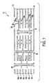
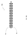
- Figure 1 is a side cross-sectional view of a multilayer printed circuit board in accordance with the present invention.
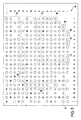
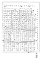
- Figure 2 shows a layout of a surface mount grid array package of an electronic component having 1247 input/output (I/O) contacts.
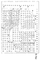
- Figure 3 shows one quadrant (i.e., the lower right quadrant) of the layout shown in Figure 2.
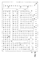
- Figure 4 shows a portion of the primary layer of the multilayer printed circuit board shown in Figure 1.
- Figure 5 shows a portion of a first power/ground plane layer of the multilayer printed circuit board shown in Figure 1.
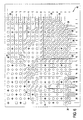
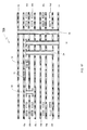
- Figure 6 shows a portion of a first signal layer of the multilayer printed circuit board shown in Figure 1.
- Figure 7 shows a portion of a second power/ground plane layer of the multilayer printed circuit board shown in Figure 1.
- Figure 8 shows a portion of a second signal layer of the multilayer printed circuit board shown in Figure 1.
- Figure 9 shows a portion of a third power/ground plane layer of the multilayer printed circuit board shown in Figure 1.
- Figure 10 shows a portion of a fourth power/ground plane layer of the multilayer printed circuit board shown in Figure 1.
- Figure 11 shows a portion of a third signal layer of the multilayer printed circuit board shown in Figure 1.
- Figure 12 shows a portion of a fifth power/ground plane layer of the multilayer printed circuit board shown in Figure 1.
- Figure 13 shows a portion of a fourth signal layer of the multilayer printed circuit board shown in Figure 1.
- Figure 14 shows a portion of a sixth power/ground plane layer of the multilayer printed circuit board shown in Figure 1.
- Figure 15 shows a portion of the secondary layer of the multilayer printed circuit board shown in Figure 1.
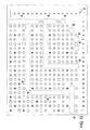
- Figure 16 shows an alternative embodiment of a portion of the primary layer of the multilayer printed circuit board shown in Figure 1.
- Figure 17 is a side cross-sectional view of another multilayer printed circuit board in accordance with the present invention.
- Figure 18A shows an electronic component having electrically conductive contacts formed on one side thereof for electrically connecting to corresponding electrically conductive contacts formed on a layer of the multilayer printed circuit board shown in Figure 17.
- Figure 18B shows an electronic component having electrically conductive contacts formed on multiple sides thereof for electrically connecting to corresponding electrically conductive contacts formed on multiple layers of the multilayer printed circuit board shown in Figure 17.
- FIG. 1 there is shown a side cross-sectional view of a multilayer printed circuit board 10 in accordance with the present invention. That is, the multilayer printed circuit board 10 incorporates the concepts of the present invention so as to reduce the number of layers in the multilayer printed circuit board 10.
- the multilayer printed circuit board 10 comprises a primary (top) layer 12, a secondary (bottom) layer 14, a plurality of signal layers 16, and a plurality of power/ground plane layers 18. It should be noted that the primary layer 12 and the secondary layer 14 are primarily power/ground plane layers except for contact pads and test signal runs formed thereon, as will be described in more detail below. It should also be noted that electronic components may be mounted on either (single-sided board) or both (double-sided board) the primary layer 12 and the secondary layer 14.
- the multilayer printed circuit board 10 also comprises a first supervia 20 for electrically connecting selected ones of the plurality of signal layers 16 (i.e., signal layers 16b and 16c), a second supervia 22 for electrically connecting the primary layer 12, the secondary layer 14, and selected ones of the plurality of power/ground plane layers 18 (i.e., power/ground plane layers 18a, 18c, 18e, and 18f), a buried via 24 for electrically connecting selected ones of the plurality of signal layers 16 (i.e., signal layers 16a and 16d), and a microvia 26 for electrically connecting signal layer 16a to a contact pad 28 formed on the primary layer 12.
- a first supervia 20 for electrically connecting selected ones of the plurality of signal layers 16 (i.e., signal layers 16b and 16c)
- a second supervia 22 for electrically connecting the primary layer 12, the secondary layer 14, and selected ones of the plurality of power/ground plane layers 18 (i.e., power/ground plane layers 18a, 18c, 18e, and 18f)
- the buried via 24 and/or the microvia 26 may alternatively be used to electrically connect selected ones of the plurality of power/ground plane layers 18.
- the microvia 26 could also be a via-in-pad, or some other similar non-through-hole via, that the microvia 26 may be formed on either or both the primary layer 12 and the secondary layer 14, and that the microvia 26 may be electrically connected to other microvias, supervias, buried vias, etc., either directly or through signal layer or power/ground plane layer electrical connections.
- microvia 26 (or substantial equivalent thereof) which allows a substantial portion of the present invention technique to be realized, as will now be described in more detail with reference to Figures 2-16, of which Figures 4-16 correspond to the twelve layers of the multilayer printed circuit board 10.
- FIG. 2 there is shown a layout 30 of a surface mount grid array package of an electronic component having 1247 input/output (I/O) contacts.
- Figure 2 also shows a legend indicating the type of signal associated with I/O contact.
- Figure 3 shows one quadrant 32 (i.e., the lower right quadrant) of the layout 30 shown in Figure 2.
- Figures 4-16 directly coincide with the quadrant 32 shown in Figure 3.
- the signal type legend in Figure 2 also applies to Figure 3, as well as to Figures 4-16.
- this portion 34 of the primary layer 12 of the multilayer printed circuit board 10 directly coincides with the quadrant 32 shown in Figure 3. That is, this portion 34 of the primary layer 12 corresponds to the portion of the multilayer printed circuit board 10 where one quadrant of an electronic component having a surface mount grid array package with 1247 I/O contacts is mounted on the multilayer printed circuit board 10.
- the primary layer 12 is primarily a power/ground plane layer except for contact pads and test signal runs formed thereon. More particularly, the primary layer 12 includes a ground plane that is electrically connected to ground contact pads (i.e., GND in legend), but is not electrically connected to power contact pads (i.e., Vdd and Vdd2 in legend), signal contact pads (i.e., signal in legend), or test contact pads (i.e., test in legend). The ground plane of the primary layer 12 is also not electrically connected to a plurality of test signal runs 36 formed on the primary layer 12.
- ground contact pads i.e., GND in legend
- Vdd and Vdd2 power contact pads
- signal contact pads i.e., signal in legend
- test contact pads i.e., test in legend
- areas 38 of the multilayer printed circuit board 10 where channels are formed in other layers of the multilayer printed circuit board 10 in accordance with the present invention. These areas 38 also indicate where microvias or via-in-pads are formed in the multilayer printed circuit board 10. That is, all of the contact pads within these areas 38 are formed as microvias or via-in-pads for facilitating the formation of channels in other layers of the multilayer printed circuit board 10 in accordance with the present invention, as described in detail below.
- this portion 40 of the power/ground plane layer 18a of the multilayer printed circuit board 10 directly coincides with the quadrant 32 shown in Figure 3. That is, this portion 40 of the power/ground plane layer 18a corresponds to the portion of the multilayer printed circuit board 10 where one quadrant of an electronic component having a surface mount grid array package with 1247 I/O contacts is mounted on the multilayer printed circuit board 10.
- the power/ground plane layer 18a is primarily a ground plane layer except for vias formed therein. More particularly, the power/ground layer 18a includes a ground plane that is electrically connected to ground vias (i.e., GND in legend), but is not electrically connected to power vias (i.e., Vdd and Vdd2 in legend) or signal vias (i.e., signal in legend). Note that there are no test vias formed in the power/ground plane layer 18a as test contact pads and test signal runs are typically only formed on the primary layer 12.
- FIG. 5 Also shown in Figure 5 are the areas 38 of the multilayer printed circuit board 10 where channels are formed in other layers of the multilayer printed circuit board 10 in accordance with the present invention. Again, these areas 38 also indicate where microvias or via-in-pads are formed in the multilayer printed circuit board 10. That is, all of the vias within these areas 38 are formed as microvias or via-in-pads for facilitating the formation of channels in other layers of the multilayer printed circuit board 10 in accordance with the present invention, as described in detail below.
- this portion 42 of the signal layer 16a of the multilayer printed circuit board 10 directly coincides with the quadrant 32 shown in Figure 3. That is, this portion 42 of the power/ground plane layer 18a corresponds to the portion of the multilayer printed circuit board 10 where one quadrant of an electronic component having a surface mount grid array package with 1247 I/O contacts is mounted on the multilayer printed circuit board 10.
- the signal layer 16a includes a plurality of electrically conductive signal runs 44 that are electrically connected to the microvias or via-in-pads in the areas 38 of the multilayer printed circuit board 10 where channels are formed in other layers of the multilayer printed circuit board 10 in accordance with the present invention.
- These signal runs 44 are typically preselected based upon the characteristics of the signals they carry. That is, the signals runs 44 may carry high speed signals. Alternatively, the signals runs 44 may carry low speed signals.
- the microvias or via-in-pads that are formed in the areas 38 of the multilayer printed circuit board 10 do not extend any further into the multilayer printed circuit board 10 than the signal layer 16a. This allows channels to be formed beneath these microvias or via-in-pads in other layers of the multilayer printed circuit board 10, as described in detail below.
- this portion 46 of the power/ground plane layer 18b of the multilayer printed circuit board 10 directly coincides with the quadrant 32 shown in Figure 3. That is, this portion 46 of the power/ground plane layer 18b corresponds to the portion of the multilayer printed circuit board 10 where one quadrant of an electronic component having a surface mount grid array package with 1247 I/O contacts is mounted on the multilayer printed circuit board 10.
- the power/ground plane layer 18b is primarily a power plane layer except for vias formed therein. More particularly, the power/ground layer 18b includes a power plane that is electrically connected to power vias (i.e., Vdd in legend), but is not electrically connected to ground vias (i.e., GND in legend) or signal vias (i.e., signal in legend). Note that there are no test vias formed in the power/ground plane layer 18b as test contact pads and test signal runs are typically only formed on the primary layer 12. Also note that there are no vias formed in the power/ground plane layer 18b in the areas 38 of the multilayer printed circuit board 10, thereby forming channels in these areas 38 in this and other layers of the multilayer printed circuit board 10 in accordance with the present invention.
- These areas 38 of the multilayer printed circuit board 10 are devoid of vias in the power/ground plane layer 18b because microvias or via-in-pads are only formed in these areas 38 of the multilayer printed circuit board 10 extending from the primary layer 12 to the signal layer 16a, as described above.
- this portion 48 of the signal layer 16b of the multilayer printed circuit board 10 directly coincides with the quadrant 32 shown in Figure 3. That is, this portion 48 of the signal layer 16b corresponds to the portion of the multilayer printed circuit board 10 where one quadrant of an electronic component having a surface mount grid array package with 1247 I/O contacts is mounted on the multilayer printed circuit board 10.
- the signal layer 16b includes a plurality of electrically conductive signal runs 50 that are electrically connected to vias formed in the signal layer 16b outside the areas 38 of the multilayer printed circuit board 10 where channels are formed in this and other layers of the multilayer printed circuit board 10.
- many of these signal runs 50 are routed in these channels. That is, the channels formed by the absence of vias in the signal layer 16b in the areas 38 of the multilayer printed circuit board 10 allow the plurality of electrically conductive signal runs 50 to be routed therein. Otherwise, if vias were present in these areas 38 in this and other layers of the multilayer printed circuit board 10, then additional signal layers would be required to route the plurality of electrically conductive signal runs 50. Thus, the absence of vias in these areas 38 in this and other layers of the multilayer printed circuit board 10 allow for an overall reduction in the number of signal layers required in the multilayer printed circuit board 10.
- the channels formed in the areas 38 of the multilayer printed circuit board 10 are beneficially arranged so as to intersect at least one edge of the grid array.
- the benefit of this arrangement is to allow the plurality of electrically conductive signal runs 50 to be more easily routed out from within the grid array.
- some of the channels formed in the areas 38 of the multilayer printed circuit board 10 intersect more than one edge of the grid array.
- These multiple edge intersecting channels are typically formed of orthogonal columns and rows, but may also be formed in diagonal or random patterns.
- the channels formed in the areas 38 of the multilayer printed circuit board 10 may have varying widths. That is, while the channels formed in the areas 38 of the multilayer printed circuit board 10 are shown in Figure 8 as having a width of one contact pad or via, the present invention is not limited in this regard.
- the channels formed in the areas 38 of the multilayer printed circuit board 10 can be two or more contact pads or vias wide depending upon how many microvias or via-in-pads are used and how many vias are removed in accordance with the practices of the present invention as described above.
- this portion 52 of the power/ground plane layer 18c of the multilayer printed circuit board 10 directly coincides with the quadrant 32 shown in Figure 3. That is, this portion 52 of the power/ground plane layer 18c corresponds to the portion of the multilayer printed circuit board 10 where one quadrant of an electronic component having a surface mount grid array package with 1247 I/O contacts is mounted on the multilayer printed circuit board 10.
- the power/ground plane layer 18c is primarily a ground plane layer except for vias formed therein. More particularly, the power/ground layer 18c includes a ground plane that is electrically connected to ground vias (i.e., GND in legend), but is not electrically connected to power vias (i.e., Vdd and Vdd2 in legend) or signal vias (i.e., signal in legend). Note that there are no test vias formed in the power/ground plane layer 18c as test contact pads and test signal runs are typically only formed on the primary layer 12.
- this portion 54 of the power/ground plane layer 18d of the multilayer printed circuit board 10 directly coincides with the quadrant 32 shown in Figure 3. That is, this portion 54 of the power/ground plane layer 18d corresponds to the portion of the multilayer printed circuit board 10 where one quadrant of an electronic component having a surface mount grid array package with 1247 I/O contacts is mounted on the multilayer printed circuit board 10.
- the power/ground plane layer 18d is primarily a power plane layer except for vias formed therein. More particularly, the power/ground layer 18d includes a power plane that is electrically connected to power vias (i.e., Vdd2 in legend), but is not electrically connected to ground vias (i.e., GND in legend) or signal vias (i.e., signal in legend). Note that there are no test vias formed in the power/ground plane layer 18d as test contact pads and test signal runs are typically only formed on the primary layer 12.
- this portion 56 of the signal layer 16c of the multilayer printed circuit board 10 directly coincides with the quadrant 32 shown in Figure 3. That is, this portion 56 of the signal layer 16c corresponds to the portion of the multilayer printed circuit board 10 where one quadrant of an electronic component having a surface mount grid array package with 1247 I/O contacts is mounted on the multilayer printed circuit board 10.
- the signal layer 16c includes a plurality of electrically conductive signal runs 58 that are electrically connected to vias formed in the signal layer 16c outside the areas 38 of the multilayer printed circuit board 10 where channels are formed in this and other layers of the multilayer printed circuit board 10.
- many of these signal runs 58 are routed in these channels. That is, the channels formed by the absence of vias in the signal layer 16c in the areas 38 of the multilayer printed circuit board 10 allow the plurality of electrically conductive signal runs 58 to be routed therein. Otherwise, if vias were present in these areas 38 in this and other layers of the multilayer printed circuit board 10, then additional signal layers would be required to route the plurality of electrically conductive signal runs 58.
- the absence of vias in these areas 38 in this and other layers of the multilayer printed circuit board 10 allow for an overall reduction in the number of signal layers required in the multilayer printed circuit board 10.
- this portion 60 of the power/ground plane layer 18e of the multilayer printed circuit board 10 directly coincides with the quadrant 32 shown in Figure 3. That is, this portion 60 of the power/ground plane layer 18e corresponds to the portion of the multilayer printed circuit board 10 where one quadrant of an electronic component having a surface mount grid array package with 1247 I/O contacts is mounted on the multilayer printed circuit board 10.
- the power/ground plane layer 18e is primarily a ground plane layer except for vias formed therein. More particularly, the power/ground layer 18e includes a ground plane that is electrically connected to ground vias (i.e., GND in legend), but is not electrically connected to power vias (i.e., Vdd and Vdd2 in legend) or signal vias (i.e., signal in legend). Note that there are no test vias formed in the power/ground plane layer 18e as test contact pads and test signal runs are typically only formed on the primary layer 12.
- this portion 62 of the signal layer 16d of the multilayer printed circuit board 10 directly coincides with the quadrant 32 shown in Figure 3. That is, this portion 62 of the signal layer 16d corresponds to the portion of the multilayer printed circuit board 10 where one quadrant of an electronic component having a surface mount grid array package with 1247 I/O contacts is mounted on the multilayer printed circuit board 10.
- the signal layer 16d includes a plurality of electrically conductive signal runs 64 that are electrically connected to vias formed in the signal layer 16d outside the areas 38 of the multilayer printed circuit board 10 where channels are formed in this and other layers of the multilayer printed circuit board 10.
- many of these signal runs 64 are routed in these channels. That is, the channels formed by the absence of vias in the signal layer 16d in the areas 38 of the multilayer printed circuit board 10 allow the plurality of electrically conductive signal runs 64 to be routed therein. Otherwise, if vias were present in these areas 38 in this and other layers of the multilayer printed circuit board 10, then additional signal layers would be required to route the plurality of electrically conductive signal runs 64. Thus, the absence of vias in these areas 38 in this and other layers of the multilayer printed circuit board 10 allow for an overall reduction in the number of signal layers required in the multilayer printed circuit board 10.
- this portion 66 of the power/ground plane layer 18f of the multilayer printed circuit board 10 directly coincides with the quadrant 32 shown in Figure 3. That is, this portion 66 of the power/ground plane layer 18f corresponds to the portion of the multilayer printed circuit board 10 where one quadrant of an electronic component having a surface mount grid array package with 1247 I/O contacts is mounted on the multilayer printed circuit board 10.
- the power/ground plane layer 18f is primarily a ground plane layer except for vias formed therein. More particularly, the power/ground layer 18f includes a ground plane that is electrically connected to ground vias (i.e., GND in legend), but is not electrically connected to power vias (i.e., Vdd and Vdd2 in legend) or signal vias (i.e., signal in legend). Note that there are no test vias formed in the power/ground plane layer 18f as test contact pads and test signal runs are typically only formed on the primary layer 12.
- this portion 68 of the secondary layer 14 of the multilayer printed circuit board 10 directly coincides with the quadrant 32 shown in Figure 3. That is, this portion 68 of the secondary layer 14 corresponds to the portion of the multilayer printed circuit board 10 where one quadrant of an electronic component having a surface mount grid array package with 1247 I/O contacts is mounted on the multilayer printed circuit board 10.
- the secondary layer 14 is primarily a power/ground plane layer except for contact pads formed thereon. More particularly, the secondary layer 14 includes a ground plane that is electrically connected to ground contact pads (i.e., GND in legend), but is not electrically connected to power contact pads (i.e., Vdd and Vdd2 in legend) or signal contact pads (i.e., signal in legend). Note that there are no test vias formed in the secondary layer 14 as test contact pads and test signal runs are typically only formed on the primary layer 12. Also note that there are no vias formed in the secondary layer 14 in the areas 38 of the multilayer printed circuit board 10, thereby forming channels in these areas 38 in this and other layers of the multilayer printed circuit board 10 in accordance with the present invention.
- These areas 38 of the multilayer printed circuit board 10 are devoid of vias in the secondary layer 14 because microvias or via-in-pads are only formed in these areas 38 of the multilayer printed circuit board 10 extending from the primary layer 12 to the signal layer 16a, as described above.
- Provisional Patent Application No. 60/212,387 all of which have been incorporated by reference herein in their entirety. All of these techniques may be implemented either manually or in an automated manner. For example, these techniques may be automated by receiving electronic component information in, for example, a design file. That is, the design file may include an electrically conductive contact count characteristic, an electrically conductive contact pitch characteristic, an electrically conductive contact signal type characteristic, and/or an electrically conductive contact signal direction characteristic for one or more electronic components. One or more electronic components having a high density electrically conductive contact array package may then be identified based at least in part upon at least one of the electrically conductive contact count characteristic or the electrically conductive contact pitch characteristic.
- Electrical signals may then be routed on a plurality of electrically conductive signal path layers in a multilayer circuit board so as to make electrical connections to and from each high density electrically conductive contact array package that is mounted on the multilayer circuit board based at least in part upon at least one of the electrically conductive contact signal type characteristic or the electrically conductive contact signal direction characteristic.
- reducing the number of layers in a multilayer printed circuit board in accordance with the present invention as described above may involve the processing of input data and the generation of output data to some extent.
- This input data processing and output data generation may be implemented in hardware or software.
- specific electronic and/or optical components may be employed in a processing device or similar or related circuitry for implementing the functions associated with reducing the number of layers in a multilayer printed circuit board in accordance with the present invention as described above.
- one or more processors operating in accordance with stored instructions may implement the functions associated with reducing the number of layers in a multilayer printed circuit board in accordance with the present invention as described above. If such is the case, it is within the scope of the present invention that such instructions may be stored on one or more processor readable carrier (e.g., a magnetic disk), or transmitted to one or more processors via one or more signals.
- processor readable carrier e.g., a magnetic disk
- one or more microvias 26 may be formed in the multilayer circuit board 10 extending from the surface 12 of the multilayer circuit board 10 to one of the plurality of electrically conductive signal path layers (e.g., 16b), wherein the microvias 26 are arranged so as to form at least one of the channels 38 in another of the plurality of electrically conductive signal path layers (e.g., 16c) located beneath the microvias 26.
- one or more microvias 26 may extend from the surface 12 of the multilayer circuit board 10 to others of the plurality of electrically conductive signal path layers (e.g., 16b, 16c, 16d) besides the uppermost electrically conductive signal path layer (i.e., 16a).
- the channels 38 may be configured to have a linear, circular, diamond, curved, stepped, staggered, and/or random shape, or a combination thereof. Also, the channels 38 may be configured to be in a vertical, horizontal, diagonal, and/or random direction, or a combination thereof. Further, one or more channels 38 may be formed such that they are totally enclosed within the array of electrically conductive contacts that are formed on the multilayer circuit board 10 for mating with the electrically conductive contacts of the electronic component (i.e., no portion of the channel is formed along the periphery of the array of electrically conductive contacts formed on the multilayer circuit board 10) (e.g., see channel 38a in Figure 16).
- one or more channels 38 may be formed such that they extend all the way across the array of electrically conductive contacts that are formed on the multilayer circuit board 10 for mating with the electrically conductive contacts of the electronic component (i.e., the channel is formed extending from one side to another side of the array of electrically conductive contacts formed on the multilayer circuit board 10). Moreover, one or more channels 38 may be formed such that only portions thereof extend to the periphery of the array of electrically conductive contacts that are formed on the multilayer circuit board 10 for mating with the electrically conductive contacts of the electronic component (i.e., at least a portion of the channel is formed along the periphery of the array of electrically conductive contacts formed on the multilayer circuit board 10).
- the electrically conductive contacts of the electronic component may have a variety of contact array patterns.
- the electrically conductive contacts of the electronic component, and hence the array of electrically conductive contacts formed on the multilayer circuit board 10 may have a square, triangular, circular, and/or random electrically conductive contact pattern, or a combination thereof.
- the electrical signals to be routed may be differential electrical signals. If such is the case, the differential electrical signals may beneficially be at least partially routed together in the channels 38 formed in the plurality of electrically conductive signal path layers 16 beneath the microvias 26, thereby enhancing signal quality.
- microvias 26 may be beneficial to form at least some of the microvias 26 outside of the array of electrically conductive contacts that are formed on the multilayer circuit board 10 for mating with the electrically conductive contacts of the electronic component.
- Figure 16 there is shown an alternative embodiment of a portion 34a of the primary layer 12 of the multilayer printed circuit board 10 wherein some of the microvias 26a are formed outside of the array of electrically conductive contacts that are formed on the multilayer circuit board 10 for mating with the electrically conductive contacts of the electronic component.
- the microvias 26a are electrically connected to corresponding peripheral ones of the electrically conductive array contacts that are formed on the multilayer circuit board 10 for mating with the electrically conductive contacts of the electronic component via electrically conductive connections 70.
- the microvias 26a may extend from the surface 12 of the multilayer circuit board 10 to any of the plurality of electrically conductive signal path layers 16.
- the peripheral electrically conductive array contacts that are connected to the microvias 26a do not extend below the primary layer 12 of the multilayer printed circuit board 10.
- additional and/or expanded channels 38a may be formed in all of the plurality of electrically conductive signal path layers 16 beneath these peripheral electrically conductive array contacts, including the uppermost electrically conductive signal path layer (i.e., 16a).
- one or more electrically conductive vias may be formed in the multilayer printed circuit board 10 extending from the surface 12 of the multilayer printed circuit board 10 to at least one of the electrically conductive power/ground layers (i.e., 18 and/or 14), wherein each of the electrically conductive vias is electrically connected to at least one respective electrically conductive power/ground contact formed on the surface 12 of the multilayer printed circuit board 10.
- Each of the electrically conductive power/ground contacts forms a portion of the electrically conductive contact array that is formed on the surface 12 of the multilayer circuit board 10 for mating with the electrically conductive power/ground contacts of the electronic component. This allows additional channels to be formed in each of the plurality of electrically conductive signal path layers 16 beneath the electrically conductive power/ground contacts.
- FIG. 17 there is shown a side cross-sectional view of an alternative multilayer printed circuit board 10a in accordance with the present invention. Similar to the multilayer printed circuit board 10 of Figure 1, the multilayer printed circuit board 10a of Figure 17 comprises a primary (top) layer 12, a secondary (bottom) layer 14, a plurality of signal layers 16, and a plurality of power/ground plane layers 18.
- the multilayer printed circuit board 10a also comprises a supervia 20 for electrically connecting the primary layer 12, the secondary layer 14, and selected ones of the plurality of power/ground plane layers 18.
- the multilayer printed circuit board 10a further comprises a plurality of buried vias 24 for electrically connecting selected ones of the plurality of signal layers 16 and selected ones of the plurality of power/ground plane layers 18.
- the multilayer printed circuit board 10a of Figure 17 comprises a blind via 74 for electrically connecting the secondary layer 14, selected ones of the plurality of signal layers 16, and selected ones of the plurality of power/ground plane layers 18.
- the multilayer printed circuit board 10a also comprises an embedded electronic component 72 disposed between the power/ground plane layer 18a and the signal layer 16a.
- the embedded electronic component 72 may be one of a wide variety of possible electronic components.
- an electronic component 72a having electrically conductive contacts 76 formed on one side thereof.
- the electrically conductive contacts 76 may electrically connect to corresponding electrically conductive contacts formed on a selected one of the plurality of signal layers 16 (i.e., layer 16a in Figure 17) or a selected one of the plurality of power/ground plane layers 18 (i.e., layer 18a in Figure 17).
- an electronic component 72b having electrically conductive contacts 76 formed on both sides thereof.
- the electrically conductive contacts 76 may electrically connect to corresponding electrically conductive contacts formed on a selected one of the plurality of signal layers 16 (i.e., layer 16a in Figure 17) and a selected one of the plurality of power/ground plane layers 18 (i.e., layer 18a in Figure 17).
- other types of electronic components e.g., discrete components
- embedded electronic components may be embedded in the multilayer printed circuit board 10a of Figure 17, and such embedded electronic components may be disposed between or on any of the plurality of signal layers 16 and/or any of the plurality of power/ground plane layers 18 in accordance with the present invention.
- the above-described techniques for reducing the number of layers in a multilayer printed circuit board may apply when such embedded electronic components are employed.
Landscapes
- Engineering & Computer Science (AREA)
- Microelectronics & Electronic Packaging (AREA)
- Manufacturing & Machinery (AREA)
- Production Of Multi-Layered Print Wiring Board (AREA)
- Structure Of Printed Boards (AREA)
Applications Claiming Priority (2)
| Application Number | Priority Date | Filing Date | Title |
|---|---|---|---|
| US10/326,123 US7069650B2 (en) | 2000-06-19 | 2002-12-23 | Method for reducing the number of layers in a multilayer signal routing device |
| US326123 | 2002-12-23 |
Publications (2)
| Publication Number | Publication Date |
|---|---|
| EP1434473A2 true EP1434473A2 (fr) | 2004-06-30 |
| EP1434473A3 EP1434473A3 (fr) | 2004-08-04 |
Family
ID=32468981
Family Applications (1)
| Application Number | Title | Priority Date | Filing Date |
|---|---|---|---|
| EP03394085A Withdrawn EP1434473A3 (fr) | 2002-12-23 | 2003-09-12 | Technique de réduction du nombre de couches dans un dispositif d'acheminement de signaux |
Country Status (6)
| Country | Link |
|---|---|
| US (1) | US7069650B2 (fr) |
| EP (1) | EP1434473A3 (fr) |
| JP (1) | JP2004207727A (fr) |
| KR (1) | KR100575041B1 (fr) |
| CN (1) | CN1510986A (fr) |
| CA (1) | CA2438751C (fr) |
Cited By (3)
| Publication number | Priority date | Publication date | Assignee | Title |
|---|---|---|---|---|
| EP1763294A1 (fr) * | 2005-09-13 | 2007-03-14 | Alcatel | Plans d'un réseau de billes (BGA) pour l'optimisation du routage sur une plaque de circuit imprimé |
| EP1631130A3 (fr) * | 2004-08-30 | 2007-08-08 | Hirose Electric Co., Ltd. | Carte de circuit imprimé à transmission |
| WO2011004224A1 (fr) * | 2009-07-06 | 2011-01-13 | Sony Ericsson Mobile Communications Ab | Boîtier de semi-conducteur doté dun agencement de contacts non uniforme |
Families Citing this family (16)
| Publication number | Priority date | Publication date | Assignee | Title |
|---|---|---|---|---|
| US7107673B2 (en) * | 2000-06-19 | 2006-09-19 | Nortel Networks Limited | Technique for accommodating electronic components on a multiplayer signal routing device |
| US20050225955A1 (en) * | 2004-04-09 | 2005-10-13 | Hewlett-Packard Development Company, L.P. | Multi-layer printed circuit boards |
| JP2006261213A (ja) * | 2005-03-15 | 2006-09-28 | Fujitsu Ltd | 電子回路 |
| JP4844080B2 (ja) * | 2005-10-18 | 2011-12-21 | 日本電気株式会社 | 印刷配線板及びその電源雑音抑制方法 |
| WO2008039526A2 (fr) * | 2006-09-25 | 2008-04-03 | Flextronics Ap, Llc | Régulateur bidirectionnel |
| WO2008057598A2 (fr) * | 2006-11-08 | 2008-05-15 | Mentor Graphics Corporation | Schémas de trous d'interconnexion de sortance disposés en alternance |
| WO2008058258A2 (fr) * | 2006-11-08 | 2008-05-15 | Mentor Graphics Corporation | Utilisation des fuites dans des modèles de cartes de circuits imprimes |
| US20090159326A1 (en) * | 2007-12-19 | 2009-06-25 | Richard Mellitz | S-turn via and method for reducing signal loss in double-sided printed wiring boards |
| US7996806B2 (en) * | 2008-02-06 | 2011-08-09 | Electronics For Imaging, Inc. | Methods and apparatus for layout of multi-layer circuit substrates |
| US8928449B2 (en) * | 2008-05-28 | 2015-01-06 | Flextronics Ap, Llc | AC/DC planar transformer |
| US8586873B2 (en) * | 2010-02-23 | 2013-11-19 | Flextronics Ap, Llc | Test point design for a high speed bus |
| JP2013093345A (ja) * | 2011-10-24 | 2013-05-16 | Hitachi Ltd | 光モジュールおよび多層基板 |
| US9565762B1 (en) * | 2013-12-06 | 2017-02-07 | Marvell Israel (M.I.S.L) Ltd. | Power delivery network in a printed circuit board structure |
| KR102339899B1 (ko) * | 2014-12-12 | 2021-12-15 | 삼성전자주식회사 | 반도체 패키지, 모듈 기판 및 이를 포함하는 반도체 패키지 모듈 |
| US10194524B1 (en) * | 2017-07-26 | 2019-01-29 | Cisco Technology, Inc. | Anti-pad for signal and power vias in printed circuit board |
| KR102385249B1 (ko) * | 2020-03-04 | 2022-04-11 | 가톨릭대학교 산학협력단 | 결막도포용 접촉식 일회용 안약용기 |
Family Cites Families (18)
| Publication number | Priority date | Publication date | Assignee | Title |
|---|---|---|---|---|
| US3300686A (en) * | 1963-07-30 | 1967-01-24 | Ibm | Compatible packaging of miniaturized circuit modules |
| FR2509563A1 (fr) * | 1981-07-10 | 1983-01-14 | Thomson Csf | Dispositif support de circuits integres utilise dans un systeme de selection de circuits integres a haute fiabilite |
| US5144746A (en) * | 1987-12-28 | 1992-09-08 | Texas Instruments Incorporated | Method of assembling compact silicon module for high density integrated circuits |
| ATE139370T1 (de) * | 1990-07-23 | 1996-06-15 | Siemens Nixdorf Inf Syst | Filmträger zur bandautomatischen verdrahtung |
| JP2739726B2 (ja) * | 1990-09-27 | 1998-04-15 | インターナシヨナル・ビジネス・マシーンズ・コーポレーシヨン | 多層プリント回路板 |
| JP2966972B2 (ja) * | 1991-07-05 | 1999-10-25 | 株式会社日立製作所 | 半導体チップキャリアとそれを実装したモジュール及びそれを組み込んだ電子機器 |
| US5784262A (en) * | 1995-11-06 | 1998-07-21 | Symbios, Inc. | Arrangement of pads and through-holes for semiconductor packages |
| US5686764A (en) * | 1996-03-20 | 1997-11-11 | Lsi Logic Corporation | Flip chip package with reduced number of package layers |
| US5847936A (en) * | 1997-06-20 | 1998-12-08 | Sun Microsystems, Inc. | Optimized routing scheme for an integrated circuit/printed circuit board |
| FR2782230B1 (fr) | 1998-08-06 | 2000-09-08 | Bull Electronics Angers | Carte de circuits imprimes |
| US6232564B1 (en) * | 1998-10-09 | 2001-05-15 | International Business Machines Corporation | Printed wiring board wireability enhancement |
| US6181004B1 (en) * | 1999-01-22 | 2001-01-30 | Jerry D. Koontz | Digital signal processing assembly and test method |
| US6198635B1 (en) * | 1999-05-18 | 2001-03-06 | Vsli Technology, Inc. | Interconnect layout pattern for integrated circuit packages and the like |
| US6689634B1 (en) | 1999-09-22 | 2004-02-10 | Texas Instruments Incorporated | Modeling technique for selectively depopulating electrical contacts from a foot print of a grid array (BGA or LGA) package to increase device reliability |
| US6256769B1 (en) * | 1999-09-30 | 2001-07-03 | Unisys Corporation | Printed circuit board routing techniques |
| US6388890B1 (en) * | 2000-06-19 | 2002-05-14 | Nortel Networks Limited | Technique for reducing the number of layers in a multilayer circuit board |
| US20030043560A1 (en) * | 2001-06-15 | 2003-03-06 | Clarkson Robert Roy | Printed circuit board having a microelectronic semiconductor device mount area for trace routing therethrough |
| US6521846B1 (en) * | 2002-01-07 | 2003-02-18 | Sun Microsystems, Inc. | Method for assigning power and ground pins in array packages to enhance next level routing |
-
2002
- 2002-12-23 US US10/326,123 patent/US7069650B2/en not_active Expired - Fee Related
-
2003
- 2003-08-29 CA CA002438751A patent/CA2438751C/fr not_active Expired - Fee Related
- 2003-08-30 KR KR1020030060483A patent/KR100575041B1/ko not_active Expired - Fee Related
- 2003-09-12 EP EP03394085A patent/EP1434473A3/fr not_active Withdrawn
- 2003-09-25 CN CNA031594573A patent/CN1510986A/zh active Pending
- 2003-12-18 JP JP2003421670A patent/JP2004207727A/ja active Pending
Cited By (4)
| Publication number | Priority date | Publication date | Assignee | Title |
|---|---|---|---|---|
| EP1631130A3 (fr) * | 2004-08-30 | 2007-08-08 | Hirose Electric Co., Ltd. | Carte de circuit imprimé à transmission |
| EP1763294A1 (fr) * | 2005-09-13 | 2007-03-14 | Alcatel | Plans d'un réseau de billes (BGA) pour l'optimisation du routage sur une plaque de circuit imprimé |
| WO2011004224A1 (fr) * | 2009-07-06 | 2011-01-13 | Sony Ericsson Mobile Communications Ab | Boîtier de semi-conducteur doté dun agencement de contacts non uniforme |
| US8093708B2 (en) | 2009-07-06 | 2012-01-10 | Sony Ericsson Mobile Communications Ab | Semiconductor package having non-uniform contact arrangement |
Also Published As
| Publication number | Publication date |
|---|---|
| US20040016117A1 (en) | 2004-01-29 |
| CA2438751A1 (fr) | 2004-06-23 |
| CN1510986A (zh) | 2004-07-07 |
| KR100575041B1 (ko) | 2006-04-28 |
| JP2004207727A (ja) | 2004-07-22 |
| HK1147641A1 (en) | 2011-08-12 |
| CA2438751C (fr) | 2008-04-08 |
| KR20040057896A (ko) | 2004-07-02 |
| EP1434473A3 (fr) | 2004-08-04 |
| US7069650B2 (en) | 2006-07-04 |
Similar Documents
| Publication | Publication Date | Title |
|---|---|---|
| US6388890B1 (en) | Technique for reducing the number of layers in a multilayer circuit board | |
| US7069650B2 (en) | Method for reducing the number of layers in a multilayer signal routing device | |
| US7256354B2 (en) | Technique for reducing the number of layers in a multilayer circuit board | |
| US20030011071A1 (en) | Semiconductor device | |
| US7069646B2 (en) | Techniques for reducing the number of layers in a multilayer signal routing device | |
| US7107673B2 (en) | Technique for accommodating electronic components on a multiplayer signal routing device | |
| JP2005166794A (ja) | 部品パッケージとプリント配線基板および電子機器 | |
| EP1434474A2 (fr) | Technique pour interconnecter électriquement des signaux électriques entre un composant électronique et un dispositif d'acheminement de signaux multicouche | |
| EP1714530B1 (fr) | Procede pouvant augmenter une densite d'acheminement d'une carte de circuit imprime, et carte de circuit imprime de ce type | |
| US8631706B2 (en) | Noise suppressor for semiconductor packages | |
| US7281326B1 (en) | Technique for routing conductive traces between a plurality of electronic components of a multilayer signal routing device | |
| CN101808479B (zh) | 减少信号布线设备中的层数的方法 | |
| EP1461985B1 (fr) | Technique pour loger des composants electroniques sur un dispositif de routage de signal multicouche | |
| US8013253B2 (en) | Electrical connection board and assembly of such a board and a semiconductor component comprising an integrated circuit chip | |
| HK1147641B (zh) | 减少信号布线设备中的层数的方法 | |
| HK1064253B (en) | Technique for reducing the number of layers in a multilayer circuit board | |
| HK1143271B (en) | Technique for accommodating electronic components on a multilayer signal routing device | |
| HK1066146A (en) | Technique for reducing the number of layers in a signal routing device |
Legal Events
| Date | Code | Title | Description |
|---|---|---|---|
| PUAI | Public reference made under article 153(3) epc to a published international application that has entered the european phase |
Free format text: ORIGINAL CODE: 0009012 |
|
| PUAL | Search report despatched |
Free format text: ORIGINAL CODE: 0009013 |
|
| AK | Designated contracting states |
Kind code of ref document: A2 Designated state(s): AT BE BG CH CY CZ DE DK EE ES FI FR GB GR HU IE IT LI LU MC NL PT RO SE SI SK TR |
|
| AX | Request for extension of the european patent |
Extension state: AL LT LV MK |
|
| AK | Designated contracting states |
Kind code of ref document: A3 Designated state(s): AT BE BG CH CY CZ DE DK EE ES FI FR GB GR HU IE IT LI LU MC NL PT RO SE SI SK TR |
|
| AX | Request for extension of the european patent |
Extension state: AL LT LV MK |
|
| 17P | Request for examination filed |
Effective date: 20050204 |
|
| AKX | Designation fees paid |
Designated state(s): DE FR GB |
|
| RBV | Designated contracting states (corrected) |
Designated state(s): DE FR GB |
|
| STAA | Information on the status of an ep patent application or granted ep patent |
Free format text: STATUS: THE APPLICATION HAS BEEN WITHDRAWN |
|
| 18W | Application withdrawn |
Effective date: 20080819 |