EP1437660A2 - Halbleiterspeicheranordnung und montierte Halbleiteranordnung - Google Patents
Halbleiterspeicheranordnung und montierte Halbleiteranordnung Download PDFInfo
- Publication number
- EP1437660A2 EP1437660A2 EP03029229A EP03029229A EP1437660A2 EP 1437660 A2 EP1437660 A2 EP 1437660A2 EP 03029229 A EP03029229 A EP 03029229A EP 03029229 A EP03029229 A EP 03029229A EP 1437660 A2 EP1437660 A2 EP 1437660A2
- Authority
- EP
- European Patent Office
- Prior art keywords
- memory
- circuit
- different
- bank
- write
- Prior art date
- Legal status (The legal status is an assumption and is not a legal conclusion. Google has not performed a legal analysis and makes no representation as to the accuracy of the status listed.)
- Withdrawn
Links
Images


Classifications
-
- G—PHYSICS
- G11—INFORMATION STORAGE
- G11C—STATIC STORES
- G11C11/00—Digital stores characterised by the use of particular electric or magnetic storage elements; Storage elements therefor
- G11C11/21—Digital stores characterised by the use of particular electric or magnetic storage elements; Storage elements therefor using electric elements
- G11C11/34—Digital stores characterised by the use of particular electric or magnetic storage elements; Storage elements therefor using electric elements using semiconductor devices
- G11C11/40—Digital stores characterised by the use of particular electric or magnetic storage elements; Storage elements therefor using electric elements using semiconductor devices using transistors
- G11C11/401—Digital stores characterised by the use of particular electric or magnetic storage elements; Storage elements therefor using electric elements using semiconductor devices using transistors forming cells needing refreshing or charge regeneration, i.e. dynamic cells
- G11C11/4063—Auxiliary circuits, e.g. for addressing, decoding, driving, writing, sensing or timing
- G11C11/407—Auxiliary circuits, e.g. for addressing, decoding, driving, writing, sensing or timing for memory cells of the field-effect type
- G11C11/4076—Timing circuits
-
- G—PHYSICS
- G11—INFORMATION STORAGE
- G11C—STATIC STORES
- G11C7/00—Arrangements for writing information into, or reading information out from, a digital store
-
- G—PHYSICS
- G06—COMPUTING OR CALCULATING; COUNTING
- G06F—ELECTRIC DIGITAL DATA PROCESSING
- G06F13/00—Interconnection of, or transfer of information or other signals between, memories, input/output devices or central processing units
- G06F13/14—Handling requests for interconnection or transfer
- G06F13/16—Handling requests for interconnection or transfer for access to memory bus
- G06F13/1668—Details of memory controller
- G06F13/1689—Synchronisation and timing concerns
-
- G—PHYSICS
- G06—COMPUTING OR CALCULATING; COUNTING
- G06F—ELECTRIC DIGITAL DATA PROCESSING
- G06F13/00—Interconnection of, or transfer of information or other signals between, memories, input/output devices or central processing units
- G06F13/14—Handling requests for interconnection or transfer
- G06F13/16—Handling requests for interconnection or transfer for access to memory bus
- G06F13/1668—Details of memory controller
- G06F13/1694—Configuration of memory controller to different memory types
-
- G—PHYSICS
- G11—INFORMATION STORAGE
- G11C—STATIC STORES
- G11C7/00—Arrangements for writing information into, or reading information out from, a digital store
- G11C7/10—Input/output [I/O] data interface arrangements, e.g. I/O data control circuits, I/O data buffers
- G11C7/1015—Read-write modes for single port memories, i.e. having either a random port or a serial port
- G11C7/1045—Read-write mode select circuits
Definitions
- the present invention relates to a semiconductor memory device which controls different types of memory devices using the same hardware, and specifically relates to a semiconductor memory device and a mount-type semiconductor device which control different types of memories such as an FCRAM (Fast cycle Random Access Memory), an NWRAM (NetWork RAM) or a DDR (Double Data Rate)-DRAM (Dynamic Random Access Memory) which are different in the AC specifications, the initial sequence, the capacity, the case size, the pin assignment, the power supply, the interface, and the like.
- FCRAM Full cycle Random Access Memory
- NWRAM Network RAM
- DDR Double Data Rate
- DRAM Dynamic Random Access Memory
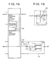
- FIGS. 1A and 1B are drawings (FIG. 6 of said JP-A) showing this semiconductor memory device.
- This semiconductor memory is a four-bank 256M bytes/128M bytes compatible SDRAM, and includes a fuse circuit of a 128M byte-adapted version 132, a selector 133 for selecting either an output signal R12T output from the fuse set circuit 132 or a row address signal RADT ⁇ 12>, and a row address latch circuit 134 which is connected to the selector 133, and a latch circuit 135, all of which are serving as an address switch circuit 131 connected between a row address buffer 105 and a repair circuit 122.
- the 128M byte-adapted version fuse set circuit 132 includes fuse set circuits 121a and 121b.
- a normally operable memory mat is arbitrarily fixed by dividing the bit line direction into 1/2, 1/4, or the like in the respective memory array banks Bank 0 to Bank 3 based on outputs of row address signals RABT ⁇ 12> and RATT ⁇ 12> of the address switch circuit 131, there by converting the 256M byte capacity into the 128M byte capacity.
- the semiconductor memory device described in this publication has the following problems. First, though it is possible to switch the capacity for the same type of memories, it is not possible to switch the capacity for different types of memories such as an FCRAM and a DDR. This is because this conventional semiconductor memory device cannot carry out the control unless the memories have the same specifications except for the memory capacity.
- a memory control circuit of a memory device including a memory device which uses the same hardware, and controls different types of memory devices such as an FCRAM or an NWRAM, and a DDR-DRAM, which are different in the AC specifications, the initial sequence, the capacity, the case size, the pin assignment, the power supply, and the interface.
- a purpose of the present invention is to provide a semiconductor memory device and a mount-type semiconductor device which can provide memory devices different in the cost and the performance simply by switching among memories different in the type using the same hardware, can thus increase the variation and property of products, and can reduce the development cost and the number of types of component parts to be used by eliminating the necessity of the development of memory devices for respective different memories, thereby reducing the cost of the component parts.
- a semiconductor memory device includes a memory; and a memory control circuit for controlling the memory.
- the memory control circuit includes a bank busy circuit for variably setting a bank busy time that controls different bank cycle times, a read data input circuit for inputting read data output from the memory in variable input timing, a write data output circuit for outputting write data to the memory in variable output timing, a command control circuit for issuing a command to the memory based on a memory command output from the bank busy circuit, thereby controlling different command interfaces, a write mask circuit for controlling different write masks, an initial sequence control circuit for controlling memories different in the initial sequence, and an address generation circuit for controlling different address interfaces.
- the memory control circuit controls different memories using the same hardware.
- the bank busy circuit includes a program register for variably setting the bank busy time, and a bank busy counter for setting a value set on the program register when a bank n is accessed for turning on, and then counting down the set value for each clock cycle.
- the bank busy counter provides the command control circuit with a memory command indicating cleared bank busy when the logic value of the bank busy counter becomes zero, thereby controlling memories different in the bank cycle time.
- the read data input circuit includes a first program register for variably setting the input timing of the read data output from the memory for controlling memories different in the access time, and inputs the read data output from the memory based on a set value on the first program register in variable input timing.
- the write data output circuit includes a second program register for variably setting the output timing of the write data output to the memory, and can adjust write data output timing based on a set value on the second program register.
- the bank busy circuit may switch the bank busy time using a switch.
- the write mask circuit relates to mask control for the write data output to the memory, and has a program register for switching between masking write operation using a variable write function when an FCRAM or an NWRAM is used, and masking the write operation using a Data Mask function when a DDR-SDRAM is used.
- the write mask circuit relates to the mask control for the write data output to the memory, and may have a switch for switching between masking of write operation using a variable Write function when an FCRAM or an NWRAM is used, and masking of the write operation using a Data Mask function when a DDR-SDRAM is used.
- the address generation circuit relates to address generation of memories different in address assignment, and includes a program register for switching address generation logic.
- the address generation circuit relates to the address generation of memories different in address assignment, and has a switch for switching the address generation logic.
- the initial sequence control circuit relates to control of memories different in the initial sequence, for example, includes a program register for variably changing the issue sequence of commands including mode register set, extension mode register set, auto refresh, and all bank pre-charge, and for variably changing set values on a mode register and an extension mode register, controls the memories different in the initial sequence using the same circuit, and issues an initial sequence command including the mode register set, the extension mode register set, the auto refresh, and the all bank pre-charge to the command control circuit.
- a program register for variably changing the issue sequence of commands including mode register set, extension mode register set, auto refresh, and all bank pre-charge, and for variably changing set values on a mode register and an extension mode register, controls the memories different in the initial sequence using the same circuit, and issues an initial sequence command including the mode register set, the extension mode register set, the auto refresh, and the all bank pre-charge to the command control circuit.
- the initial sequence control circuit relates to the control of the memories different in the initial sequence, may include a switch for variably changing the issue sequence of commands including the mode register set, the extension mode register set, the auto refresh, and the all bank pre-charge, and for variably changing the set values on the mode register and the extension mode register, controls the memories different in the initial sequence using the same circuit, and issues an initial sequence command including the mode register set, the extension mode register set, the auto refresh, and the all bank pre-charge to the command control circuit.
- the semiconductor memory device comprises a power supply capable of adjusting a power supply output level supplied for the memory.
- a power supply capable of adjusting a power supply output level supplied for the memory.
- the mount of a different memory can be handled only by changing a memory power supply of a power supply unit without changing a board for mounting the memory.
- a mount-type semiconductor device is a mount-type semiconductor device for mounting the above-described semiconductor memory device on a board.
- the memory is different in the package size or the pin assignment, and only a board for mounting the memory is changed, and one type of mother board is used for connecting the board for mounting the memory thereon when the memory different in the package size or the pin assignment is mounted.
- the board for mounting the memory thereon is a DIMM (Dual Inline Memory Module), for example.
- a mount-type semiconductor device is a mount-type semiconductor device for mounting the above-described semiconductor memory device on a board.
- the memory is different in whether a terminating resistor is incorporated or not, and when the memory which is different in whether a terminating resistor is incorporated or not is mounted, a terminating resistor is not mounted on a DIMM (Dual Inline Memory Module) for the memory incorporating a terminating resistor, a terminating resistor is attached to a DIMM for the memory not incorporating a terminating resistor, and one type of mother board is provided for connecting to the board for mounting the memory thereon.
- DIMM Direct Inline Memory Module
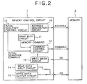
- FIG. 2 is a block diagram showing a semiconductor memory device according to an embodiment of the present invention.
- a memory control circuit 1 controls a memory 2 of this semiconductor memory device.
- a bank busy circuit 11 of this memory control circuit 1 can variably set a bank busy time for controlling different bank cycle times, thereby controlling memories having different bank cycle times.
- a read data input circuit 14 variably changes input timing of read data output from the memory 2.
- a write data output circuit 13 variably changes output timing of write data output to the memory.
- a command control circuit 12 can control different command interfaces.
- a write mask circuit 15 can control different write masks.
- An initial sequence circuit 17 can control memories having different initial sequences.
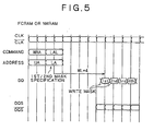
- An address generation circuit 16 can control different address interfaces. When signals shown in FIG. 5 are connected to this memory control circuit 1, the memory control circuit 1 can control different memories 2 using the same hardware.
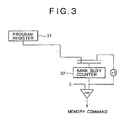
- FIG. 3 shows a block diagram showing the specific construction of the bank busy circuit 11.
- the bank busy circuit 11 which controls memories different in the bank cycle time includes a program register 31 which can variably set the bank busy time, and a bank busy counter 32 which sets a value set on the program register and counts down the set value every clock cycle when a bank n (n ⁇ 1) is accessed for turning on. In this way, when the count of the bank busy counter 32 becomes logical zero, bank busy is cleared, and thus the bank busy circuit 11 issues a memory command to the command circuit 12.
- the value of the bank busy counter 32 is not logical zero, since the status is bank busy, and the bank busy circuit 11 controls the bank cycle by not issuing the memory command.
- the read data input circuit 14 includes a first program register (not shown) for variably setting input timing of read data output from the memory 2 for controlling memories different in the access time, and inputs the read data output from the memory based on a set value of the first program register.
- the write data output circuit 13 includes a second program register (not shown) for variably setting the output timing of the write data output to the memory, and adjusts write data output timing based on a set value on the second program register.
- the write mask circuit 15 relates to mask control of the write data to the memory, outputs a Variable Write signal to the command circuit 12 for masking write operation when an FCRAM or an NWRAM is used, and outputs a Data Mask signal for masking the write operation when a DDR-SDRAM is used. In this way, the memory is controlled during the write mask operation.
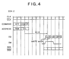
- the command control circuit 12 inputs the variable write signal from the write mask circuit 15, outputs a signal shown in a time chart of FIG. 4 when a DDR-SDRAM is used, and outputs a signal shown in a time chart of FIG. 5 when an FCRAM or an NWRAM is used.
- the write mask circuit 15 masks the write operation using the Data Mask function when a DDR-SDRAM is used, and masks the write operation using the variable Write function when an FCRAM or an NWRAM is used.
- the correspondence of the pin assignments is controlled by switching as shown in FIG. 6.
- the address generation circuit 16 relates to address generation for memory devices different in address assignment, and switches address generation logic using a program register (not shown).
- the initial sequence control circuit 17 relates to control of memory devices different in the initial sequence, includes a program register (not shown) for variably controlling the issue sequence of commands including mode register set, extension mode register set, auto refresh, all bank pre-charge, and for variably changing set values on a mode register and an extension mode register, controls the memories different in the initial sequence using the same circuit, and issues an initial sequence command including the mode register set, the extension mode register set, the auto refresh, and the all bank pre-charge to the command control circuit 12.
- a program register (not shown) for variably controlling the issue sequence of commands including mode register set, extension mode register set, auto refresh, all bank pre-charge, and for variably changing set values on a mode register and an extension mode register
- reference numeral 22 denotes a board; 23, a power supply layer for a memory device inside the board; 25, a DIMM (Dual Inline Memory Module); and 26, a memory control LSI.
- DIMM Dual Inline.Memory Module
- FIG. 8 and FIG. 9 show the pin assignments (I/O pin definition).
- FIG. 8 shows a 512Mb ⁇ 8, 4-BANK, BL4 FCRAM
- FIG. 9 shows a 512Mb ⁇ 8, 4-BANK, BL4 DDR2.
- row address inputs are referred to as RDA and WRA for the FCRAM, and ACT, MRS, and REF for the DDR2.
- Column address inputs are referred to as LAL, REF, and MRS for the FCRAM, and RDA and WTA for the DDR2.
- CLK and CLK' can be realized using the same hardware both for the FCRAM and the DDR2, and a DQ pin can also be realized using the same hardware both for the FCRAM and the DDR2. Since a CS pin requires a "L" output both for the FCRAM and the DDR2 during the row address input, and requires the "L” output only for the DDR2 during the column address input, the CS pin can be controlled easily in terms of the hardware quantity and the delay.
- the DM pin In terms of the presence/absence of a DM pin, while the DM pin is used for the write mask function for the DDR2, the DM pin is not used for the FCRAM.
- the FCRAM When the FCRAM is used, an A0-1 field and A13-A14 are used to specify respective write masks for a fast half and a last half. According to the above described control, the two types of memory devices can be easily controlled in terms of the delay using the small amount of hardware.
- a terminating resistor is not mounted on the DIMM for the memory incorporating a terminating resistor, and a terminating resistor is mounted on the DIMM for the memory not incorporating a terminating resistor, thereby using only one type of mother board connected to the board for the memory mount.
- the same hardware can control various types of memories such as the FCRAM or the NWRAM and the DDR-DRAM different in the AC specifications, the initial sequence, the capacity, the case size, the pin assignment, the power supply, the interface, and the like.
- switches may be used as hardware to switch the bank busy time, the mask function applied to the write operation, the address generation logic, and the like.
Landscapes
- Engineering & Computer Science (AREA)
- Theoretical Computer Science (AREA)
- Physics & Mathematics (AREA)
- General Engineering & Computer Science (AREA)
- General Physics & Mathematics (AREA)
- Microelectronics & Electronic Packaging (AREA)
- Computer Hardware Design (AREA)
- Dram (AREA)
- Static Random-Access Memory (AREA)
- Memory System (AREA)
Applications Claiming Priority (2)
| Application Number | Priority Date | Filing Date | Title |
|---|---|---|---|
| JP2002382326 | 2002-12-27 | ||
| JP2002382326A JP2004213337A (ja) | 2002-12-27 | 2002-12-27 | 半導体記憶装置及び実装型半導体装置 |
Publications (2)
| Publication Number | Publication Date |
|---|---|
| EP1437660A2 true EP1437660A2 (de) | 2004-07-14 |
| EP1437660A3 EP1437660A3 (de) | 2006-10-04 |
Family
ID=32501156
Family Applications (1)
| Application Number | Title | Priority Date | Filing Date |
|---|---|---|---|
| EP03029229A Withdrawn EP1437660A3 (de) | 2002-12-27 | 2003-12-18 | Halbleiterspeicheranordnung und montierte Halbleiteranordnung |
Country Status (6)
| Country | Link |
|---|---|
| US (1) | US20040136258A1 (de) |
| EP (1) | EP1437660A3 (de) |
| JP (1) | JP2004213337A (de) |
| KR (1) | KR100604429B1 (de) |
| AU (1) | AU2003271387A1 (de) |
| CA (1) | CA2453695A1 (de) |
Cited By (3)
| Publication number | Priority date | Publication date | Assignee | Title |
|---|---|---|---|---|
| WO2011049753A1 (en) * | 2009-10-21 | 2011-04-28 | Micron Technology, Inc. | Memory having internal processors and methods of controlling memory access |
| CN103810123A (zh) * | 2014-02-18 | 2014-05-21 | 龙芯中科技术有限公司 | 内存控制装置及方法 |
| US9495242B2 (en) | 2014-07-30 | 2016-11-15 | International Business Machines Corporation | Adaptive error correction in a memory system |
Families Citing this family (8)
| Publication number | Priority date | Publication date | Assignee | Title |
|---|---|---|---|---|
| US6728150B2 (en) * | 2002-02-11 | 2004-04-27 | Micron Technology, Inc. | Method and apparatus for supplementary command bus |
| US7093156B1 (en) * | 2002-05-13 | 2006-08-15 | Virage Logic Corp. | Embedded test and repair scheme and interface for compiling a memory assembly with redundancy implementation |
| JP2006059046A (ja) * | 2004-08-19 | 2006-03-02 | Nec Computertechno Ltd | メモリの制御方式およびメモリ制御回路 |
| JP2007066026A (ja) * | 2005-08-31 | 2007-03-15 | Renesas Technology Corp | 半導体装置とその試験方法及び製造方法 |
| KR100843142B1 (ko) | 2006-09-19 | 2008-07-02 | 삼성전자주식회사 | 반도체 메모리 장치 및 이를 포함하는 메모리 시스템 |
| US8004884B2 (en) * | 2009-07-31 | 2011-08-23 | International Business Machines Corporation | Iterative write pausing techniques to improve read latency of memory systems |
| US8374040B2 (en) | 2011-02-25 | 2013-02-12 | International Business Machines Corporation | Write bandwidth in a memory characterized by a variable write time |
| US20150234726A1 (en) * | 2014-02-19 | 2015-08-20 | Brian P. Moran | Apparatus, system and method to provide platform support for multiple memory technologies |
Family Cites Families (10)
| Publication number | Priority date | Publication date | Assignee | Title |
|---|---|---|---|---|
| JPH0212541A (ja) * | 1988-04-29 | 1990-01-17 | Internatl Business Mach Corp <Ibm> | コンピユーテイング・システム及びその動作方法 |
| US5418924A (en) * | 1992-08-31 | 1995-05-23 | Hewlett-Packard Company | Memory controller with programmable timing |
| US5721860A (en) * | 1994-05-24 | 1998-02-24 | Intel Corporation | Memory controller for independently supporting synchronous and asynchronous DRAM memories |
| US5982655A (en) * | 1998-09-29 | 1999-11-09 | Cisco Technology, Inc. | Method and apparatus for support of multiple memory types in a single memory socket architecture |
| US6438670B1 (en) * | 1998-10-02 | 2002-08-20 | International Business Machines Corporation | Memory controller with programmable delay counter for tuning performance based on timing parameter of controlled memory storage device |
| JP2000132994A (ja) * | 1998-10-28 | 2000-05-12 | Hitachi Ltd | 半導体記憶装置 |
| KR100351053B1 (ko) * | 2000-05-19 | 2002-09-05 | 삼성전자 주식회사 | 종단저항을 내장하는 메모리 모듈 및 이를 포함하여 다중채널구조를 갖는 메모리 모듈 |
| US6681293B1 (en) * | 2000-08-25 | 2004-01-20 | Silicon Graphics, Inc. | Method and cache-coherence system allowing purging of mid-level cache entries without purging lower-level cache entries |
| JP4025002B2 (ja) * | 2000-09-12 | 2007-12-19 | 株式会社東芝 | 半導体記憶装置 |
| US6621754B1 (en) * | 2002-07-10 | 2003-09-16 | Micro-Star Int'l Co., Ltd. | Memory interface control circuit |
-
2002
- 2002-12-27 JP JP2002382326A patent/JP2004213337A/ja active Pending
-
2003
- 2003-12-17 CA CA002453695A patent/CA2453695A1/en not_active Abandoned
- 2003-12-18 EP EP03029229A patent/EP1437660A3/de not_active Withdrawn
- 2003-12-22 KR KR1020030094544A patent/KR100604429B1/ko not_active Expired - Fee Related
- 2003-12-24 AU AU2003271387A patent/AU2003271387A1/en not_active Abandoned
- 2003-12-24 US US10/743,919 patent/US20040136258A1/en not_active Abandoned
Cited By (6)
| Publication number | Priority date | Publication date | Assignee | Title |
|---|---|---|---|---|
| WO2011049753A1 (en) * | 2009-10-21 | 2011-04-28 | Micron Technology, Inc. | Memory having internal processors and methods of controlling memory access |
| US8719516B2 (en) | 2009-10-21 | 2014-05-06 | Micron Technology, Inc. | Memory having internal processors and methods of controlling memory access |
| US9164698B2 (en) | 2009-10-21 | 2015-10-20 | Micron Technology, Inc. | Memory having internal processors and methods of controlling memory access |
| CN103810123A (zh) * | 2014-02-18 | 2014-05-21 | 龙芯中科技术有限公司 | 内存控制装置及方法 |
| CN103810123B (zh) * | 2014-02-18 | 2017-12-29 | 龙芯中科技术有限公司 | 内存控制装置及方法 |
| US9495242B2 (en) | 2014-07-30 | 2016-11-15 | International Business Machines Corporation | Adaptive error correction in a memory system |
Also Published As
| Publication number | Publication date |
|---|---|
| CA2453695A1 (en) | 2004-06-27 |
| EP1437660A3 (de) | 2006-10-04 |
| US20040136258A1 (en) | 2004-07-15 |
| KR20040060744A (ko) | 2004-07-06 |
| KR100604429B1 (ko) | 2006-07-25 |
| AU2003271387A1 (en) | 2004-07-15 |
| JP2004213337A (ja) | 2004-07-29 |
Similar Documents
| Publication | Publication Date | Title |
|---|---|---|
| US12182397B2 (en) | Apparatuses and methods for configurable memory array bank architectures | |
| US6526473B1 (en) | Memory module system for controlling data input and output by connecting selected memory modules to a data line | |
| KR100389928B1 (ko) | 액티브 터미네이션 제어를 위한 반도체 메모리 시스템 | |
| US7911862B2 (en) | Latency control circuit and method thereof and an auto-precharge control circuit and method thereof | |
| KR101318116B1 (ko) | 집적 메모리 코어 및 메모리 인터페이스 회로 | |
| US6981100B2 (en) | Synchronous DRAM with selectable internal prefetch size | |
| US7003684B2 (en) | Memory control chip, control method and control circuit | |
| US9576639B2 (en) | Method for controlling a semiconductor device having CAL latency function | |
| JP4080892B2 (ja) | マルチビットプリフェッチ出力データパス | |
| US7221617B2 (en) | Backwards-compatible memory module | |
| JPH04229487A (ja) | ダイナミックramを含むメモリサブシステムのリフレッシュ動作制御システムを有するディジタルコンピュータ及びリフレッシュ動作制御方法 | |
| US7580319B2 (en) | Input latency control circuit, a semiconductor memory device including an input latency control circuit and method thereof | |
| EP1437660A2 (de) | Halbleiterspeicheranordnung und montierte Halbleiteranordnung | |
| CN118092581A (zh) | 用于以时钟发射操作模式的设备和方法 | |
| KR100711100B1 (ko) | 메모리 모듈 및 이를 구비하는 메모리 시스템 | |
| KR20090114940A (ko) | 반도체 메모리 소자와 그의 구동 방법 및 압축 테스트 방법 | |
| US7405992B2 (en) | Method and apparatus for communicating command and address signals | |
| KR100520597B1 (ko) | 어드레스 공간을 변경할 수 있는 반도체 기억 장치 | |
| GB2388691A (en) | Clocking memory banks out of phase to reduce the output noise | |
| US6504767B1 (en) | Double data rate memory device having output data path with different number of latches | |
| Mladenov et al. | Bandwidth, Area Efficient and Target Device Independent DDR SDRAM Controller | |
| JP2007200359A (ja) | 記憶装置、アドレス制御方法及びシステム | |
| CN120255791A (zh) | 存储芯片和存储系统 | |
| KR100543205B1 (ko) | 데이터 프리페치 방식을 달리하는 복수 소자를 지원할 수 있는 단일의 컬럼 카운터 회로 | |
| NAYAK | SDR Synchronous Dynamic Random Access Memory Controller Using Adaptive Bank Management |
Legal Events
| Date | Code | Title | Description |
|---|---|---|---|
| PUAI | Public reference made under article 153(3) epc to a published international application that has entered the european phase |
Free format text: ORIGINAL CODE: 0009012 |
|
| AK | Designated contracting states |
Kind code of ref document: A2 Designated state(s): AT BE BG CH CY CZ DE DK EE ES FI FR GB GR HU IE IT LI LU MC NL PT RO SE SI SK TR |
|
| AX | Request for extension of the european patent |
Extension state: AL LT LV MK |
|
| RIC1 | Information provided on ipc code assigned before grant |
Ipc: G11C 11/413 20060101ALI20060613BHEP Ipc: G06F 13/16 20060101AFI20040514BHEP |
|
| PUAL | Search report despatched |
Free format text: ORIGINAL CODE: 0009013 |
|
| AK | Designated contracting states |
Kind code of ref document: A3 Designated state(s): AT BE BG CH CY CZ DE DK EE ES FI FR GB GR HU IE IT LI LU MC NL PT RO SE SI SK TR |
|
| AX | Request for extension of the european patent |
Extension state: AL LT LV MK |
|
| AKX | Designation fees paid |
Designated state(s): DE FR NL SE |
|
| STAA | Information on the status of an ep patent application or granted ep patent |
Free format text: STATUS: THE APPLICATION IS DEEMED TO BE WITHDRAWN |
|
| 18D | Application deemed to be withdrawn |
Effective date: 20070405 |