EP1439385A1 - Procédé et appareil pour la détection électro-optique rapide et en ligne de défauts de tranches de semi-conducteur - Google Patents
Procédé et appareil pour la détection électro-optique rapide et en ligne de défauts de tranches de semi-conducteur Download PDFInfo
- Publication number
- EP1439385A1 EP1439385A1 EP03250255A EP03250255A EP1439385A1 EP 1439385 A1 EP1439385 A1 EP 1439385A1 EP 03250255 A EP03250255 A EP 03250255A EP 03250255 A EP03250255 A EP 03250255A EP 1439385 A1 EP1439385 A1 EP 1439385A1
- Authority
- EP
- European Patent Office
- Prior art keywords
- wafer
- view
- dies
- objects
- detectors
- Prior art date
- Legal status (The legal status is an assumption and is not a legal conclusion. Google has not performed a legal analysis and makes no representation as to the accuracy of the status listed.)
- Granted
Links
- 230000007547 defect Effects 0.000 title claims abstract description 112
- 238000000034 method Methods 0.000 title claims abstract description 104
- 238000001514 detection method Methods 0.000 title abstract description 39
- 239000011159 matrix material Substances 0.000 claims abstract description 154
- 238000007689 inspection Methods 0.000 claims abstract description 67
- 238000005286 illumination Methods 0.000 claims abstract description 56
- 238000003384 imaging method Methods 0.000 claims abstract description 47
- 238000012545 processing Methods 0.000 claims abstract description 41
- 230000003287 optical effect Effects 0.000 claims description 51
- 239000004065 semiconductor Substances 0.000 claims description 34
- 230000007246 mechanism Effects 0.000 claims description 14
- 230000003213 activating effect Effects 0.000 claims description 3
- 238000003491 array Methods 0.000 claims description 3
- 230000001360 synchronised effect Effects 0.000 abstract description 15
- 238000012634 optical imaging Methods 0.000 abstract description 14
- 238000000386 microscopy Methods 0.000 abstract description 4
- 235000012431 wafers Nutrition 0.000 description 356
- 239000013078 crystal Substances 0.000 description 39
- 238000010586 diagram Methods 0.000 description 22
- 238000004519 manufacturing process Methods 0.000 description 22
- 230000008569 process Effects 0.000 description 16
- 238000012937 correction Methods 0.000 description 13
- 238000013519 translation Methods 0.000 description 8
- 230000035945 sensitivity Effects 0.000 description 6
- 238000004891 communication Methods 0.000 description 5
- 230000003247 decreasing effect Effects 0.000 description 5
- 239000011521 glass Substances 0.000 description 5
- 238000012360 testing method Methods 0.000 description 5
- 239000011248 coating agent Substances 0.000 description 4
- 238000000576 coating method Methods 0.000 description 4
- WYTGDNHDOZPMIW-RCBQFDQVSA-N alstonine Natural products C1=CC2=C3C=CC=CC3=NC2=C2N1C[C@H]1[C@H](C)OC=C(C(=O)OC)[C@H]1C2 WYTGDNHDOZPMIW-RCBQFDQVSA-N 0.000 description 2
- 238000004458 analytical method Methods 0.000 description 2
- 238000013459 approach Methods 0.000 description 2
- 230000015572 biosynthetic process Effects 0.000 description 2
- 210000004027 cell Anatomy 0.000 description 2
- 238000005516 engineering process Methods 0.000 description 2
- 238000012986 modification Methods 0.000 description 2
- 230000004048 modification Effects 0.000 description 2
- 238000012544 monitoring process Methods 0.000 description 2
- 230000001133 acceleration Effects 0.000 description 1
- 230000009471 action Effects 0.000 description 1
- 230000004075 alteration Effects 0.000 description 1
- 230000000712 assembly Effects 0.000 description 1
- 238000000429 assembly Methods 0.000 description 1
- 238000006243 chemical reaction Methods 0.000 description 1
- 238000012790 confirmation Methods 0.000 description 1
- 230000008878 coupling Effects 0.000 description 1
- 238000010168 coupling process Methods 0.000 description 1
- 238000005859 coupling reaction Methods 0.000 description 1
- 230000007423 decrease Effects 0.000 description 1
- 230000000593 degrading effect Effects 0.000 description 1
- 238000013461 design Methods 0.000 description 1
- 238000011161 development Methods 0.000 description 1
- 210000002287 horizontal cell Anatomy 0.000 description 1
- 238000012886 linear function Methods 0.000 description 1
- 230000007257 malfunction Effects 0.000 description 1
- 239000000463 material Substances 0.000 description 1
- 230000000737 periodic effect Effects 0.000 description 1
- 238000004886 process control Methods 0.000 description 1
- 230000001902 propagating effect Effects 0.000 description 1
- 238000000275 quality assurance Methods 0.000 description 1
- 238000003908 quality control method Methods 0.000 description 1
- 239000002994 raw material Substances 0.000 description 1
- 230000003252 repetitive effect Effects 0.000 description 1
- 229910052710 silicon Inorganic materials 0.000 description 1
- 239000010703 silicon Substances 0.000 description 1
- 239000007787 solid Substances 0.000 description 1
- 238000010561 standard procedure Methods 0.000 description 1
Images

Classifications
-
- G—PHYSICS
- G01—MEASURING; TESTING
- G01N—INVESTIGATING OR ANALYSING MATERIALS BY DETERMINING THEIR CHEMICAL OR PHYSICAL PROPERTIES
- G01N21/00—Investigating or analysing materials by the use of optical means, i.e. using sub-millimetre waves, infrared, visible or ultraviolet light
- G01N21/84—Systems specially adapted for particular applications
- G01N21/88—Investigating the presence of flaws or contamination
- G01N21/95—Investigating the presence of flaws or contamination characterised by the material or shape of the object to be examined
- G01N21/956—Inspecting patterns on the surface of objects
- G01N21/95607—Inspecting patterns on the surface of objects using a comparative method
-
- G—PHYSICS
- G01—MEASURING; TESTING
- G01N—INVESTIGATING OR ANALYSING MATERIALS BY DETERMINING THEIR CHEMICAL OR PHYSICAL PROPERTIES
- G01N21/00—Investigating or analysing materials by the use of optical means, i.e. using sub-millimetre waves, infrared, visible or ultraviolet light
- G01N21/84—Systems specially adapted for particular applications
- G01N21/88—Investigating the presence of flaws or contamination
- G01N21/95—Investigating the presence of flaws or contamination characterised by the material or shape of the object to be examined
- G01N21/9501—Semiconductor wafers
Definitions
- the present invention relates to methods and systems for electro-optically detecting fabrication defects, which are random in nature, in semiconductor patterned structures such as a semiconductor wafer featuring integrated circuit dies or chips.
- the present invention relates to a method and system for fast on-line electro-optical detection of wafer defects by illuminating with a short light pulse from a pulsed laser, a field of view of an electro-optical camera system having microscopy optics, and imaging, a moving wafer, on to a focal plane assembly (FPA) optically forming a surface of photo-detectors at the focal plane of an optical imaging system, formed from several detector ensembles, each detector ensemble including an array of several two-dimensional matrix photo-detectors, where each two-dimensional matrix photo-detector produces an electronic image featuring a matrix of picture elements (pixels), such that the simultaneously created images from the different matrix photo-detectors are processed in parallel using conventional image processing techniques, for comparing the imaged field of view with another field of view serving as a reference, in order to find
- 'wafer' refers to, and is generally considered to feature individual patterned structures, known as 'semiconductor wafer dice', 'wafer dice', or wafer chips'.
- Current semiconductor technology involves the physical division of a single wafer into identical dies for the manufacture of integrated circuit chips, such that each die becomes an individual integrated circuit chip having a specific pattern, such as a memory chip or a microprocessor chip, for example.
- the type of chip produced from a given die is not relevant to the method or system of the present invention.
- the term ' field of view' refers to that part or segment of, a wafer, in general, and a wafer die, in particular, illuminated by a pulsed laser and imaged by the electro-optical camera system inspection optics in conjunction with the FPA. Accordingly, an entire single wafer die, and therefore, an entire single wafer featuring a plurality of wafer dies, is inspected by sequential imaging of a plurality or sequence of fields of view.
- the field of view can be considered as the inspection system electro-optical imaging footprint on the wafer or wafer die. Successive fields of view created while the wafer is moving in one direction are referred to as a 'strip' of fields of view.
- Pixels are referred to with respect to forming an image of a field of view by the electro-optical inspection system.
- general order of magnitude of the size of a typically square wafer die within a wafer is 1 centimeter by 1 centimeter, or 104 microns by 104 microns.
- detection of a 'wafer defect' refers to the detection of the presence of an irregularity or difference in the comparison of like patterns of wafer dies or like patterns of fields of view.
- Current methods and systems of defect detection on wafers are usually based on the analysis of comparing signals obtained from a number of adjacent wafer dies or fields of view, featuring a like pattern. Defects produced during wafer fabrication are assumed to be random in nature. Therefore, defect detection is based on a statistical approach, whereby the probability that a random defect will exist at the same location within adjacent wafer dies is very low. Hence, defect detection is commonly based on identifying irregularities through the use of the well known method of die-to-die comparison.
- a given inspection system is programmed to inspect the pattern of a wafer die or field of view, typically referred to as the inspected pattern, and then compares it to the identical pattern of a second wafer die or field of view on the same wafer, serving as the reference pattern, to detect any pattern irregularity or difference which would indicate the possible presence of a wafer defect.
- a second comparison between the previously designated inspected pattern and the like pattern of a third wafer die or field of view is performed, in order to confirm the presence of a defect and to identify the wafer die or field of view containing the defect.
- the first wafer die or field of view is considered a reference and the third wafer die or field of view is considered as inspected.
- Fabrication of semiconductor wafers is highly complex and very expensive, and the miniature integrated circuit patterns of semiconductor wafers are highly sensitive to process induced defects, foreign material particulates, and equipment malfunctions. Costs related to the presence of wafer defects are multiplied several fold when going from development stages to mass production stages. Therefore, the semiconductor industry critically depends on a very fast ramp-up of wafer yield at the initial phase of production, and then achieving and controlling a continuous high yield during volume production.
- Automated wafer inspection systems are used for quality control and quality assurance of wafer fabrication processes, equipment, and products. Such systems are used for monitoring purposes and are not directly involved in the fabrication process. As for any principle component of an overall manufacturing system, it is important that a wafer inspection method, and system of implementation, be cost effective relative to the overall costs of manufacturing semiconductor wafers.
- a notable limitation of current methods and systems of wafer defect detection relates to registration of pixel positions in wafer images.
- wafer defects can be detected by standard techniques of comparing differences in pixel intensities of an image of a targeted or inspected wafer die to pixel intensities of an image of a reference wafer die
- the pixel positions of the images of the inspected and reference wafer die need to be registered. Due to typical mechanical inaccuracies during movement of a wafer held on a translation stage, velocity of a wafer beneath a wafer inspection camera system is not constant. As a result of this, image pixel positions in the fields of a detector are distorted and may not be as initially programmed. Therefore, a best fit two-dimensional translation pixel registration correction is performed.
- Prior art methods and systems of wafer defect detection featuring a combination of continuous wafer illumination and acquiring a two dimensional image by either scanning a wafer in two dimensions using a laser flying spot scanner as taught in US Patent No. 5,699,447, issued to Alumot et al., or scanning a wafer in one dimension using a linear array of photo detectors as taught in US Pat. No. 4,247,203, issued to Levy et al., require a registration correction for all pixels or all pixel lines. These methods limit system speed, i.e. inspection throughput, and require substantial electronic hardware. Moreover, they result in residual misregistration, since no correction procedure is accurate for all pixels in an image. Residual misregistration significantly reduces system defect detection sensitivity. For a wafer inspection method or system in which all focal plane assembly pixels in any given field can be considered one unit, generated simultaneously, there is no need for image pixel registration within a field of view of a focal plane assembly.
- the photomask can not be moved a distance of more than one pixel or the image becomes smeared. Therefore, the time to scan and inspect the photomask is very long. Since the photomask is moved continuously while the two dimensional images are generated, it is necessary that the photomask move without jitter and accelerations. This motion restriction requires a very massive and accurate air-bearing stage for holding and moving the photomask, which is costly.
- the wafer inspection apparatus of Levy et al. is capable of detecting 2.5 micron defects with 95 % probability of detection on photomasks. For critical dimensions of current semiconductor integrated circuits approaching 0.1 micron, this means that the inspecting pixel must be of similar size magnitude. Since inspection speed increases inversely with squared pixel size, the apparatus of Levy et al. would slow down by more than two orders of magnitude. Furthermore, it becomes impractical to implement a motion stage capable of meeting the required mechanical accuracies.
- Wafer inspection has also been implemented using a single imaging and detection channel, based on a solid state camera using a two dimensional CCD matrix photo- detector, such as described in 'Machine Vision and Applications', (1998) 1: 205-221, by IBM scientists Byron E. Dom et al..
- a wafer inspection system designated as P300 is described for inspecting patterned wafers having a repetitive pattern of cells within each die, such as in semiconductor wafers for memory devices.
- the system captures an image field of view having 480 by 512 pixels.
- the image processing algorithms assume a known horizontal cell periodicity, R, in the image, and analyzes each pixel in the image by comparing it with two pixels, one pattern repetition period, R, away in either horizontal direction.
- Such a comparison of like cells within a single image is called a cell-to-cell comparison.
- the pixel under test is compared with periodic neighbors on both sides to resolve the ambiguity that would exist if it were compared with only a single pixel. While this system is capable of simultaneously capturing a two dimensional image of the object under test, it is very slow in inspecting an entire wafer.
- a preferred embodiment of the present invention relates to a method and system for fast on-line electro-optical detection of wafer die defects by illuminating with a short light pulse from a pulsed laser, a field of view of an electro-optical camera system having microscopy optics, and imaging a moving wafer, on to a focal plane assembly optically forming a surface of photo-detectors at the focal plane of an optical imaging system, formed from several, for example six detector ensembles, each detector ensemble including an array of several, for example, four, two-dimensional charge coupled device (CCD) matrix photo-detectors, whereby each two-dimensional CCD matrix photo-detector produces an electronic image containing a large matrix of, for example, two million, pixels, such that the simultaneously created images from the different CCD matrix detectors are processed in parallel using conventional image processing techniques, for comparing the imaged field of view with another field of view serving as a reference, in order to find differences in corresponding pixels, indicative of the presence of a wafer die defect.
- CCD charge
- the method and system of the present invention preferably enable capturing high pixel density, large field of view images of a wafer die, on-the-fly, without stopping movement of the wafer.
- High accuracy of wafer motion speed is not needed, and a relatively simple inexpensive mechanical stage for moving the wafer can be used.
- the continuously moving wafer is illuminated with a laser pulse of such short duration, for example, ten nanoseconds, significantly shorter than the image pixel dwell time, that there is effectively no image smear during the wafer motion.
- a wafer die image moves less than a tenth of a pixel.
- the laser pulse has sufficient energy and brightness to impart the necessary illumination to the inspected field of view required for creating an image of the inspected wafer die.
- processing time of an entire array of for example twenty-four CCD matrix photo-detectors, having imaging capacity of 48 megapixels is equivalent to processing time of a single CCD matrix photo-detector of the order of 1/30 of a second, since the processing of all the photo-detectors is processed in parallel. Consequently, parallel processing of the entire focal plane assembly including twenty-four CCD matrix photo-detectors provides an overall pixel processing data rate of nearly 1.5 gigapixels per second.
- the overall wafer inspection system operates essentially at 100 % efficiency, whereby, the laser pulse rate of 30 pulses per second is synchronized with the frame speed of 30 frames per second of each CCD matrix photo-detector, and the wafer is moved at a linear speed such that the distance between successive fields of view is covered in 1/30 of a second.
- the method and system of the present invention preferably provide significant improvements over currently used methods and systems for electro-optical inspection and detection of wafer defects, in the semiconductor wafer fabrication industry, including providing high resolution large field of view wafer die images at very high wafer inspection throughput, and requiring less electronic and system hardware.
- the method and system of the present invention prevents misregistration of pixel positions in the wafer die images, enabling enhanced defect detection sensitivity.
- Such a method and system of wafer defect detection results in faster, more efficient, and cost effective, feedback control of wafer fabrication processes.
- a method for electro-optically inspecting a patterned semiconductor wafer of dies for a defect comprising the steps of: (a) moving the patterned wafer along an inspection path; (b) providing a repetitively pulsed laser illuminating source; (c) sequentially illuminating each of a plurality of fields of view in each of a plurality of the wafer dies by using the pulsed laser illuminating source; (d) sequentially acquiring an image of the each of the plurality of the sequentially illuminated fields of view in each of a plurality of the wafer dies by using an electro-optical camera including at least two two-dimensional matrix photo-detectors, the at least two two-dimensional matrix photo-detectors simultaneously acquiring images of each of the plurality of the sequentially illuminated fields of view in each of a plurality of the wafer dies; and (e) detecting a wafer defect by comparing the sequentially acquired images of each of the plurality of
- the repetitively pulsed laser is a Q switched Nd:YAG laser or an Excimer laser.
- the Q switched Nd:YAG laser is optically pumped by light emitting diodes.
- the electro-optical camera further includes a non-linear optical crystal functioning as a second harmonic generating crystal, placed in a laser beam light path of the repetitively pulsed laser illumination source, the non-linear optical crystal halving wavelengths of the laser beam light generated by the repetitively pulsed laser.
- the electro-optical camera may also include an additional non-linear optical crystal in order to divide the original laser wavelength by 3, thereby to generate a third harmonic, or by 4, thereby to generate a fourth harmonic.
- a system for electro-optically inspecting a patterned semiconductor wafer of dies for a defect comprising: (a) a mechanism for providing movement of the patterned wafer along an inspection path; (b) a repetitively pulsed laser illumination source for illuminating the patterned wafer; (c) an electro-optical camera including at least two two-dimensional matrix photo-detectors for sequentially acquiring an image of each of a plurality of sequentially illuminated fields of view in each of a plurality of the wafer dies, the at least two two-dimensional matrix photo-detectors operate with a mechanism for simultaneous acquisition of images of each of the plurality of the sequentially illuminated fields of view in each of a plurality of the wafer dies; and (d) an image processing mechanism for processing the sequentially acquired images of each of the plurality of the illuminated fields of view in each of a plurality of the wafer dies and detecting a wafer defect by comparing the sequentially acquired images using
- an electro-optical camera for inspecting a patterned semiconductor wafer of dies for a defect, comprising a focal plane assembly including at least one detector ensemble, the detector ensemble includes an array of at least two two-dimensional matrix photo-detectors operating with a mechanism for simultaneous acquisition of images of each of a plurality of illuminated fields of view in each of a plurality of the wafer dies.
- Implementation of the method and system of the present invention involves performing or completing tasks or steps manually, automatically, or a combination thereof.
- several steps of the present invention could be implemented by hardware or by software on any operating system of any firmware or a combination thereof.
- indicated steps of the invention could be implemented as a chip or a circuit.
- indicated steps of the invention could be implemented as a plurality of software instructions being executed by a computer using any suitable operating system.
- indicated steps of the method of the invention could be described as being performed by a data processor, such as a computing platform for executing a plurality of instructions.
- the present invention preferably comprises a method and system for fast on-line electro-optical detection of wafer defects.
- the method and system for fast on-line electro-optical detection of wafer defects of the present invention introduces the unique combination of a new imaging system featuring an optically formed surface of photo-detectors at the focal plane formed from an array of several two-dimensional matrix photo-detectors for acquiring a high resolution, high pixel density, large field of view image of a wafer die, synchronized with an illumination system featuring illumination of the wafer die by a short light pulse from a repetitively pulsed laser.
- the laser light pulse duration is significantly shorter than the image pixel dwell time, where the pixel dwell time refers to the time a point on the wafer is imaged by a detector pixel while the wafer is moving, and the laser light pulse rate is synchronized with the frame speed of the individual matrix photo-detectors.
- FIG. 1 is a flow diagram of a preferred embodiment of a method for fast electro-optical on-line detection of wafer defects.
- each generally applicable, principle step of the method of the present invention is numbered and enclosed inside a frame. Sub-steps representing further of an indicated principle step of the method are indicated by a letter in parentheses.
- FIGS. 2 through 6 are schematic diagrams illustrating exemplary preferred embodiments of the system, and of system components, for implementing the method for fast on-line electro-optical detection of wafer defects of the present invention. System components shown in FIGS. 2 through 6 corresponding to the method of FIG. 1 are referred to in the description of FIG. 1. Details and specific examples of system components of FIGS. 2 through 6 are provided throughout the following description. Terminology and references appearing in the following description of FIG. 1 are consistent with those shown in FIGS. 2 - 6.
- Step 1 of the method a patterned semiconductor wafer 12 featuring a plurality of wafer dies 14, is placed and aligned on a continuous moving XY translation stage 16.
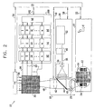
- system 10 of FIG. 2 is a schematic diagram illustrating an exemplary preferred embodiment of the system for fast on-line electro-optical detection of wafer defects.
- XY translation stage 16 moves wafer 12 in a serpentine pattern beneath an optical imaging system 18.
- Movement of XY translation stage 16, and therefore movement of wafer 12, are synchronized, by a central control system 20 via control / data links 22, with action of a multi-component camera system in a way that wafer 12 moves the equivalent of one field of view 24 during a CCD matrix photo-detector frame time of 33 milli-seconds and only a fraction, for example, on the order of about 10-2 of a single pixel during exposure to an illumination system 26, thereby resulting in no image smear or loss of image resolution.
- a multi-component electro-optical camera system including (a) an illumination system 26, (b) an optical imaging system 18, (c) an automatic focusing system 7, (d) a focal plane assembly 30, and (e) respective system control / data links, in communication with central control system 20.
- an illumination system 26 including a repetitively pulsed laser 32, a laser beam expander 34, a laser beam light path 36, and control / data links 38.
- This type of illumination system enables ultra fast imaging of a large field of view 24, by featuring pulsed laser 32 for repetitively generating and propagating a highly bright and highly energetic light pulse in an extremely short period of time.
- Illumination system 26 is in communication with the central control system 20 via control / data links 38.
- pulse rate i.e., pulses per second
- pulsed laser 32 is synchronized with frame speed of the array of individual matrix photo-detectors of focal plane assembly 30.
- a relatively large number of pixels for example, about forty eight million pixels, of focal plane assembly array 30 of several, for example, twenty four, matrix photo-detectors, is simultaneously illuminated, and there is essentially no relative movement among the pixels.
- the laser light pulse duration is significantly shorter than the image pixel dwell time, where the pixel dwell time refers to the time a point on the wafer is imaged by a detector pixel while the wafer is moving.
- repetitively pulsed laser 32 is a Q switched Nd:YAG laser, optically pumped by light emitting diodes, at a pulse rate of 30 pulses per second, with a pulse time interval of about 10 nanoseconds, generating a pulsed monochromatic light beam at a wavelength of 1.06 microns.
- the pulse rate of pulsed laser illumination system 26 of 30 pulses per second is synchronized with a frame speed of 30 frames per second, of the array of CCD matrix photo-detectors on focal plane assembly 30.
- Laser 32 may also be an Excimer laser.
- Optical resolution is a linear function of the illuminating wavelength. Resolution of an optical system increases as illumination wavelength decreases. Therefore, to increase resolution of optical system 18 and consequently defect detection sensitivity of inspection system 10, one or more crystals 40 having non linear optical properties and generating at least a 'second harmonic' may be placed in laser beam light path 36 of illumination system 26.
- the second, third or fourth harmonic generated by the crystal or crystals 40 provides illumination with a 0.53 micron, 0.355 micron or 0.265 micron wavelength, respectively, thereby doubling, tripling or quadrupling, respectively, the resolution of the wafer inspection system 10.
- an optical imaging system 18 including a focusing lens 42, a beam splitter 44, an objective lens 46, and control / data links 49.
- This system is suitable for ultra fast high resolution synchronous imaging of high magnification, for example, 50X, of wide field of view 24 of a wafer die 14.
- An automatic focusing system 28 automatically adjusts and sets the position of objective lens 46 of optical imaging system 18 for optimum focus of all wafer dies 14 on wafer 12.
- Optical imaging system 18 is in communication with the central control system 20 via control / data links 49.
- focusing lens 42 images laser light 48, where laser light 48 represents light reflected, scattered and diffracted by wafer 12, onto focal plane assembly 30. This imaging process is further described with reference to FIG. 5A below.
- an automatic focusing system 28 including sensor and control devices (not shown) is provided, which, via optical imaging system 18, automatically maintains wafer 12, and therefore, a wafer die 14, in focus.
- a focal plane assembly 30 including a number of detector ensembles 50 (FIGS. 4 - 5), where each detector ensemble 50 features several individual two-dimensional matrix photo-detectors, preferably but not limited to, at least two two-dimensional CCD matrix photo-detectors 52 (FIGS. 3A - 3B), focal plane assembly electronics 54, and control / data links 56, 58, and 90, enabling high capacity and ultra fast high resolution synchronous imaging of a wafer die 14.
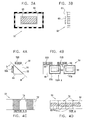
- FIGS. 3A and 3B, FIGS. 4A through 4D, and FIGS. 5A and 5B are schematic diagrams illustrating close-up views of an individual CCD matrix photo-detector 52, a detector ensemble 50 and focal plane assembly 30, respectively.
- FIGS. 3A - 3B of schematic diagrams illustrating top and side views of a two-dimensional CCD matrix photo-detector 52, respectively, photo-sensitive area 60 is surrounded by a photo-insensitive area 62, a configuration which prevents the physical placement of two CCD matrix photo-detectors side-by-side, thus creating a preferably, but not limited to, continuous, photo-sensitive focal plane.
- Focal plane assembly 30 (FIGS. 2 and 5A) includes several, for example, six, detector ensembles 50 (FIGS.
- each detector ensemble 50 includes several, for example, four, two-dimensional CCD matrix photo-detectors 52, for a total of, for example, twenty four, commercially available high resolution, black and white, silicon two-dimensional CCD matrix photo-detectors 52, wherein each CCD matrix photo-detector 52 has a very high number of, for example, 1940 x 1035 (i.e., on the order of two million or 2 mega) image sensing picture elements, or pixels, capable of providing 30 frames per second at high definition standards.
- each CCD matrix photo-detector 52 has a very high number of, for example, 1940 x 1035 (i.e., on the order of two million or 2 mega) image sensing picture elements, or pixels, capable of providing 30 frames per second at high definition standards.
- Focal plane assembly 30, featuring six detector assemblies 50, each detector ensemble featuring an array 64 (FIG. 4D) of four individual CCD matrix photo-detectors 52, optically couples all twenty-four individual CCD matrix photo-detectors 52 to optically form a, preferably, but not limited to, continuous, surface of photo-detectors 66 at the focal plane (FIG. 5B), filling the relatively large field of view 24 of the 50X magnification microscopy optical imaging system 18.
- This optical configuration enables illumination of a wafer die 14 with a single laser pulse and simultaneous imaging by an array 66, of twenty-four two-dimensional CCD matrix photo-detectors, having a total of about 48 million (48 mega) pixels.
- Focal plane assembly 30 is in communication with central control system 20 via control / data links 56 and 58 (FIG. 2).
- FIGS. 4A and 4B are schematic diagrams illustrating close-up side views of detector ensemble 50, showing geometric configuration of two sets of, for example, two CCD matrix photo-detectors each 52A and 52B.
- each detector ensemble 50 is constructed from two glass prisms 68 and 70, each prism having a right angle and a 45 degrees diagonal surface.
- Diagonal surface 72 of prism 68 has zones on which a highly reflective coating, preferably approaching 100%, are applied.
- On each prism 68 and 70 at least one CCD matrix photo detector is optically bonded.
- Exemplary set of two CCD matrix photo-detectors 52A bonded on prism 68 is identical to exemplary set of two CCD matrix photo-detectors 52B bonded on prism 70.
- FIG. 1 Exemplary set of two CCD matrix photo-detectors 52A bonded on prism 68 is identical to exemplary set of two CCD matrix photo-detectors 52B bonded on prism 70.
- the set of two CCD matrix photo-detectors 52A are shown bonded in straight file on prism 68, and the set of two CCD matrix photo-detectors 52B are bonded in straight file on prism 70, and the exact position of the bonded CCD matrix photo-detectors is selected such that all photo-sensitive areas 60 of individual CCD matrix photo-detectors 52A and 52B optically appear as one continuous straight strip when viewed from View A.
- FIG. 4C is a schematic diagram illustrating a close-up view of diagonal surface 72, of glass prism 68, including zones of highly reflective coating.
- FIG. 4C shows a view of Section B-B of FIG. 4A, wherein zones 74, on diagonal surface 72, are coated with highly reflective coating, and are arranged on surface 72 to be opposite photo-sensitive areas 60 of CCD matrix photo detectors 52A bonded on prism 68.
- Light entering detector ensemble 50 along View A, opposite reflective zones 74 are reflected by reflective zones 74 and deviated by 90 degrees to impinge upon CCD matrix photo-detectors 52A.
- Light entering detector ensemble 50 along View A, not opposite reflective zones 74 pass through prisms 68 and 70 undeviated and impinge upon CCD matrix photo-detectors 52B.
- FIG. 4D is a schematic diagram illustrating a close-up front optical view, of detector ensemble 50 shown in FIGS. 4A - 4C, showing the appearance of an optically continuous surface of photo-detectors, featuring the plurality of CCD matrix photo detectors 52.
- FIG 4D shows View A of FIG. 4B and demonstrates the creation by optical means of continuous surface 64, featuring four photo-sensitive photo-detector areas 60. Within surface 64, those photo-sensitive areas 60 opposite reflecting zones 74 are associated with CCD matrix photo-detectors 52A bonded onto prism 68. The other photo-sensitive areas 60 not opposite reflecting zones 74 are associated with CCD matrix photo-detectors 52B, bonded onto prism 70. Photo-detectors 52A and 52B are in different surfaces or planes and photosensitive areas 60 are not continuous, but detector ensemble 50 creates surface 64 by optical means.
- FIG. 5A is a schematic diagram illustrating a close-up view of focal plane assembly 30, including beam splitting prisms 76 and 78, and detector ensembles 50.
- focal plane assembly 30 includes six detector ensembles 50, two labeled 50A, two labeled 50B, and two labeled 50C.
- Light 48 representing reflected, scattered, and diffracted laser illumination light coming off of wafer 12, is directed and focused into focal plane assembly 30 by focusing lens 42.
- Light 48 passes through beam splitting glass cube 76 which reflects, at 90 degrees, approximately 33% of light 48, forming imaging channel 80, and transmits about 67% of light 48.
- Transmitted light 82 emerging from beam splitting cube 76 goes through a second beam splitting cube 78 which reflects, at 90 degrees, approximately 50% of light 82, forming imaging channel 84, and transmits about 50% of light 82, forming imaging channel 86.
- This configuration of the combination of beam splitting cubes 76 and 78 creates three imaging channels 80, 86 and 84, each with equal light energy, and each with approximately 33% of the light energy of original input light beam 48.
- Optical cube 88 is inserted in imaging channel 80 so as to equalize the amount of glass in the optical paths of all three imaging channels, thus enabling similar image quality formed in all three channels.
- two sets of detector ensembles 50 are placed. One set of two detector ensembles 50A is placed in imaging channel 80, one set of two detector ensembles 50B is placed in imaging channel 86, and one set of two detector ensembles 50C is placed in imaging channel 84.
- FIG. 5B is a schematic diagram illustrating front optical View A of focal plane assembly 30 demonstrating optical formation of continuous surface 66 of photo-detectors at the focal plane, by using six detector ensembles 50 and twenty-four two-dimensional CCD matrix photo-detectors 52 located in different geometrical surfaces.
- control / data links including 38, 49, 54, 56, and 58, and central control system 20, feature electronic interconnections among the different systems and system components, enabling proper automation and synchronization of the various steps of the method of detection of wafer defects.
- automatic movement of wafer 12 via movement of XY translation stage 16 is electronically set at a linear speed such that wafer 12 moves a distance of one field of view 24 between the time of two pulses emitted by pulsed laser 32 in illumination system 26.
- Temporally gated opening and closing, or frame speed, of focal plane assembly 30, including all CCD matrix photo-detectors 52 is synchronized with the pulse rate of pulsed laser 32 in illumination system 26.
- Step 3 the camera system of Step 2 is adjusted, focused, and set to a position over an inspected field of view 24 within a wafer die 14, via central control system 20 signals.
- Pulse rate of pulsed laser 32 in illumination system 26 is synchronized with the frame speed of CCD matrix photo-detectors 52 included in detector ensembles 50A, 50B, and 50C of focal plane assembly 30.
- This step is performed in order to enable movement of wafer 12, and therefore, of an inspected wafer die 14, at a speed such that an inspected field of view 24 is covered during the time interval of one frame of CCD matrix photo-detectors 52 of focal plane assembly 30.
- Step 4 instantaneous illumination of an inspected field of view 24 of an inspected wafer die 14 of Step 3 is achieved by generating a laser pulse onto inspected wafer die 14, for a time duration, for example, ten nanoseconds, orders of magnitude less than synchronized pulse rate and frame time of camera system CCD matrix photo-detectors 52, via a central control system 20 signal.
- a time duration for example, ten nanoseconds, orders of magnitude less than synchronized pulse rate and frame time of camera system CCD matrix photo-detectors 52, via a central control system 20 signal.
- a ten nanosecond laser pulse about 48 million pixels, of focal plane assembly 30 featuring twenty-four CCD matrix photo-detectors 52, is simultaneously illuminated, and there is no relative movement among the pixels.
- the laser pulse duration is much shorter than the pixel dwell time, which is the time a point on the wafer is imaged by a detector pixel while the wafer moves, and therefore, there is effectively no image smear degrading image resolution, as is typically the case in wafer inspection methods and systems featuring continuous illumination of a wafer.
- Step 5 illuminated inspected field of view 24 of Step 4 is imaged by optical imaging system 18 onto focal plane assembly 30, optically linked to detector ensembles 50A, 50B, and 50C, featuring the twenty-four, two dimensional CCD matrix photo-detectors 52, via central control system 20 signal.
- Step 6 the digital image (not shown) of Step 5, featuring about 58 million pixels, of an inspected field of view 24 of a wafer die 14 is acquired by using focal plane assembly 30 optically forming a, preferably, but not limited to, continuous surface of at least two two-dimensional CCD matrix photo-detectors 52, by synchronized opening of temporally gated CCD matrix photo-detectors 52, via a central control system 20 signal.
- focal plane assembly 30 optically forming a, preferably, but not limited to, continuous surface of at least two two-dimensional CCD matrix photo-detectors 52, by synchronized opening of temporally gated CCD matrix photo-detectors 52, via a central control system 20 signal.
- a central control system 20 signal a central control system 20 signal.
- sub-step (a) acquired digital image data is grabbed via a set of parallel configured image processing channels 90 by an image grabber 92, and is saved in an image memory buffer 94, part of image processing system 100 (FIG. 2).
- Step 7 Step 3 through Step 6 are sequentially repeated for image acquisition of the next fields of view within the same inspected wafer die 14, thereby forming a strip of fields of views until and including the first equivalent field of view of the nearest neighboring wafer die in the strip, serving as a reference.
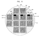
- FIG. 6 is a schematic diagram illustrating a close-up view of the image acquisition process featuring wafer dies, where each wafer die is sequentially inspected by imaging a plurality or strips of fields of view, one field of view at a time.
- FIG. 6 following image acquisition of first field of view 24A in first inspected wafer die 6A, there is image acquisition of second field of view 24B in same first inspected wafer die 14A.
- image processing system 100 includes parallel configured image processing channels 90 for image grabbing by an image grabber 92, an image buffer 94, a defect detection unit 96, a defect file 98, and control / data links 102.
- Image data acquired by focal plane assembly 30 featuring twenty-four two-dimensional CCD matrix photo-detectors 52 is processed in parallel, whereby each of the twenty-four CCD matrix photo-detectors 52 communicates separately, in parallel to the other CCD matrix photo-detectors 52 of focal plane assembly 30, with image grabber 92, via twenty-four separate image processing channels 90.
- each of the twenty-four separate image processing channels 90 having about 2 megapixels of image data, acquired at a rate of 30 times per second, is used for processing at a moderate rate of 60 megapixels per second.
- Image processing system 100 is in communication with central control system 20 via control / data links 102.
- Step 8 includes sub-step (a) performing an image alignment between the inspected field of view and the reference field of view, sub-step (b) identifying the presence of a potential wafer defect, sub-step (c) saving the comparison data in a defect file, and sub-step (d) deleting unneeded image data of the first field of view of the first inspected wafer die.
- an image alignment is performed between the image of each inspected field of view and the corresponding field of view serving as a reference, prior to identifying the presence of a potential wafer defect in the inspected wafer die. Due to minor mechanical inaccuracies during movement of XY translation stage 16, velocity of a wafer 12 beneath camera optical imaging system 18 is not constant. As a result of this, image pixel positions in the multiple fields of the CCD matrix detectors may not be as initially programmed according to inter-system synchronization. Therefore, a two-dimensional translational image alignment correction between an inspected field of view and a reference field of view is performed. More complex rotation registration correction may also be performed, but for standard implementation of the method and system of the present invention, it is neglected.
- FIG. 6 This process of aligning images of fields of views, prior to defect detection by image comparison is illustrated in FIG. 6 for exemplary strips 110 of equivalent fields of view.
- Pixel positions in the image of first field of view 24A of first inspected wafer die 14A and pixel positions in the image of equivalently located first field of view 24J of nearest neighboring wafer die 14B are extracted from image buffer 94, and are subjected to an image alignment correction.
- first field of view 24J of nearest neighboring wafer die 14B serves as the reference to equivalent field of view 24A of first inspected wafer die 14A.
- sub-step (b) of Step 8 following image alignment correction, there is identification of the presence of a potential wafer defect in the inspected wafer die, by comparing differences of pixel intensities of the image of each, starting from the first, field of view of the inspected wafer die to pixel intensities of the image of each equivalently located, starting from the first, field of view of the nearest neighboring wafer die.
- a standard algorithm of defect detection is used, which is based on the analysis of comparing pixel intensities of images acquired from identical fields of view of adjacent neighboring wafer dies, featuring a like pattern. Defect detection is based on a statistical approach, whereby the probability that a defect will exist at the equivalent location within adjacent wafer dies is very low.
- An exemplary standard algorithm for locating irregularities among pixel intensities of different images is based on a three-die comparison.
- the overall wafer inspection system is programmed to inspect the pattern, pixel-by-pixel, of a wafer die or field of view, typically referred to as the inspected pattern, and then compares it to the supposedly equivalent pattern of the adjacent neighboring wafer die on the same wafer, which serves as a reference.
- a defect detector detects any pattern irregularity or difference which would indicate the possible presence of a wafer defect in the current inspected wafer die.
- the pattern under test is also compared with the equivalently located pattern of another adjacent wafer die in order to resolve ambiguity that may exist if the test pattern was compared with only a single pattern. In the second comparison, in order to maintain symmetry, the pattern under test serves as the reference.
- FIG. 6 This image comparison process, performed by defect detection unit 96 (FIG. 2) is illustrated in FIG. 6. Each pixel intensity in the image of first field of view 24A of first inspected wafer die 14A is compared to the pixel intensity in the image of equivalently located first field of view 24J of adjacent neighboring wafer die 14B.
- sub-step (c) according to pre-determined comparison criteria, such as a specified difference or irregularity threshold level, a difference or irregularity in intensity of the two corresponding pixels in equivalently located first fields of view 24A, and 24J, of wafer dies 14A, and 14B acting as a reference, respectively, is saved in wafer defect file 98, in order to be further processed by a decision step confirming or dismissing defect existence and location (Step 10).
- pre-determined comparison criteria such as a specified difference or irregularity threshold level
- sub-step (d) unneeded image data of first field of view 24A of first inspected wafer die 14A is deleted from image buffer 94.
- image data of first field of view 24A of first inspected wafer die 14A is no longer needed for image processing of successive wafer dies 14 in wafer 12.
- Step 9 Step 7 and Step 8 are repeated for sequential fields of view in second inspected wafer die 14B, until and including processing the image of first field of view 24N of third inspected wafer die 14C. Steps 7 and 8 are carried out in parallel. While image acquisition in Step 7 is carried out for each field of view in a strip 110, image processing and comparison of each preceding field of view in a strip 110 is carried out according to Step 8.
- Step 10 is a decision and confirmation step, performed by defect detector unit 96, deciding and confirming whether or not there is detection of a wafer defect in each field of view, starting with field of view 24J of wafer die 14B, initially processed according to Step 8. Presence of irregularity or difference between equivalently located first fields of view 24A and 24J of first and second wafer dies 14A and 14B respectively, is followed by the next comparison between equivalently located first fields of view 24J and 24N of second and third wafer dies 14B and 14C, respectively, in order to confirm or dismiss the presence of a defect located in field of view 24J of wafer die 14B.
- confirmed wafer defect information including location of the confirmed wafer defect, is appropriately saved in defect file 98 for possible use in feedback control of a wafer fabrication process.
- Step 11 Step 7 through Step 10 are repeated, sequentially, for inspection of each field of view in a field of view strip 110 within the same wafer.
- wafer field of view 24K in wafer die 14B becomes the next inspected field of view to be subjected to image processing by Step 7 through Step 10.
- images of successive fields of view in second wafer die 14B are to be compared to equivalently located images of fields of view in wafer dies 14A and 14C.
- Field of view 24K in wafer die 14B is compared to equivalently located field of view 24B in wafer die 14A, with field of view 24B serving as the reference, and field of view 24K in wafer die 14B is compared to field of view 24P in wafer die 14C, with field of view 24K serving as a reference.
- each image of each successive set of fields of view in a strip 110 is compared once to an equivalent field of view on a wafer die proceeding it in the strip and once compared to an equivalent field of view on a wafer die succeeding it in the strip.
- Each compared field of view serves once as a reference field of view in the comparison and once as an inspected field of view in the comparison.
- Synchronized with serpentine motion of wafer 12 selection, illumination, imaging, acquisition, and processing, of an image of successive fields of view of successive wafer dies, one after another, progresses from wafer die to wafer die throughout entire wafer 12, until all wafer dies 14 of wafer 12 are inspected for defects.
- an inspection system for inspecting objects including multiple identical regions including an imager operative to image the multiple identical regions of the objects, while the objects are illuminated and are in motion along a travel path, a transporter for providing relative motion between the imager and the objects along the travel path, a pulsed laser object illuminator for illuminating the objects as they travel along the travel path and an imaging comparator for comparing images of individual ones of the multiple identical regions.
- the inspection system may include one, some or all of the following features:
- an inspection system for inspecting objects including multiple identical regions including an imager operative to image the multiple identical regions of the objects, while the objects are illuminated and are in motion along a travel path, the imager employing at least one two-dimensional detector array, a transporter for providing relative motion between the imager and the objects along the travel path, an object illuminator for illuminating the objects as they travel along the travel path, and an imaging comparator for comparing images of individual ones of the multiple identical regions.
- the inspection system may include one, some or all of the following features:
- an inspection system for inspecting objects including multiple identical regions, the system including an imager operative to image the multiple identical regions of the objects, while the objects are illuminated and are in motion along a travel path, a transporter for providing relative motion between the imager and the objects along the travel path, a laser object illuminator for illuminating the objects as they travel along the travel path, and an imaging comparator for comparing images of individual ones of the multiple identical regions.
- This system may include one, some or all of the following features:
- an inspection method for inspecting objects including multiple identical regions including using an imager for imaging the multiple identical regions of the objects, while the objects are illuminated and are in motion along a travel path, providing relative motion between the imager and the objects along the travel path, illuminating the objects as they travel along the travel path; and comparing images of individual ones of the multiple identical regions.
- the providing step may include displacing the objects along the travel path.
- the providing step may include providing continuous relative motion between the imager and the objects along the travel path.
- the inspection method may include one, some or all of the following features:
- an inspection method for inspecting objects including multiple identical regions including using an imager for imaging the multiple identical regions of the objects, while the objects are illuminated and are in motion along a travel path, employing at least one two-dimensional detector array, providing relative motion between the imager and the objects along the travel path, illuminating the objects as they travel along the travel path, and comparing images of individual ones of the multiple identical regions.
- the imaging step may employ a plurality of two-dimensional detector arrays which are arranged to be optically contiguous. Illuminating may be effected with a pulsed laser illuminator.
- Providing relative motion may include displacing the objects along the travel path.
- Providing relative motion may include providing continuous relative motion between the imager and the objects along the travel path.
- This method may also include one or more of the following features:
- an inspection method for inspecting objects including multiple identical regions including using an imager for imaging the multiple identical regions of the objects, while the objects are illuminated and are in motion along a travel path, providing relative motion between the imager and the objects along the travel path, illuminating the objects as they travel along the travel path and comparing images of individual ones of the multiple identical regions.
- the method may include one or more of the following features:
- an optical inspection system for a microscopic patterned object including a two-dimensional imager operative to image sequential portions of the microscopic patterned object, apparatus for translating the microscopic patterned object relative to the two-dimensional imager, including an illumination trigger operative to generate an illumination activating signal each time the apparatus for translating has brought the object to a new imaging position vis a vis the two-dimensional imager, an illumination source providing an illumination pulse responsive to the illumination trigger; and image acquisition apparatus operative to acquire an image of a portion of the object from the two-dimensional imager responsive to the illumination trigger.
- This system may include one or more of the following features:
- a method for electro-optically inspecting a patterned semiconductor wafer of dies for a defect including providing a repetitively pulsed laser illuminating source, illuminating at least one field of view in each of a plurality of wafer dies using the pulsed laser illuminating source, acquiring images of the at least one field of view in each of the plurality of wafer dies; and detecting a wafer defect by comparing the images using a die-to-die comparison method.
- This method may include one or more of the following features:
- a system for electro-optically inspecting a patterned semiconductor wafer of dies for a defect including a repetitively pulsed laser illuminating source, illuminating at least one field of view in each of a plurality of wafer dies, a camera, acquiring images of the at least one field of view in each of the plurality of wafer dies; and a wafer defect detector, detecting a wafer defect by comparing the images using a die-to-die comparison method.
- This system may include one or more of the following features:
- an electro-optical device for inspecting a patterned semiconductor wafer containing dies for a defect including a focal plane assembly including at least one detector ensemble including an array of at least two two-dimensional matrix photo-detectors operating with a mechanism for simultaneous acquisition of images of each of at least one illuminated field of view, and preferably a plurality thereof, in each of a plurality of dies.
- each of the at least two two-dimensional matrix photo-detectors includes a two-dimensional CCD matrix photo-detector.
- the focal plane assembly optically forms a surface of the at least two two-dimensional matrix photo-detectors at a focal plane within the electro-optical device.
- the electro-optical camera further includes a non-linear optical crystal functioning as a second harmonic generating crystal, placed in a laser beam light path of the repetitively pulsed laser illuminating source, the non-linear optical crystal halving wavelengths of the laser beam light generated by the repetitively pulsed laser.
- a non-linear optical crystal functioning as a second harmonic generating crystal
- a method for electro-optically inspecting a patterned semiconductor wafer containing dies for a defect including providing a focal plane assembly including at least one detector ensemble including an array of at least two two-dimensional matrix photo-detectors; and simultaneously acquiring images of each of at least one illuminated field of view in each of a plurality of dies.
- a system for electro-optically inspecting a patterned semiconductor wafer of dies for a defect including (a) a mechanism for providing movement of the patterned wafer along an inspection path, (b) a repetitively pulsed laser illumination source for illuminating the patterned wafer, (c) an electro-optical camera including at least two two-dimensional matrix photo-detectors for sequentially acquiring an image of each of a plurality of sequentially illuminated fields of view in each of a plurality of the wafer dies, the at least two two-dimensional matrix photo-detectors operate with a mechanism for simultaneous acquisition of images of the each of the plurality of the sequentially illuminated fields of view in each of a plurality of the wafer dies; and (d) an image processing mechanism for processing the sequentially acquired images of the each of the plurality of the illuminated fields of view in each of a plurality of the wafer dies and detecting a wafer defect by comparing the sequentially acquired images using a
- the electro-optical camera may further include a non-linear optical crystal functioning as a second harmonic generating crystal, placed in a laser beam light path of the repetitively pulsed laser illumination source, the non-linear optical crystal halving wavelengths of the laser beam light generated by the repetitively pulsed laser.
- the electro-optical camera may further include a focal plane assembly, the focal plane assembly includes at least one detector ensemble, the detector ensemble includes an array of the at least two two-dimensional matrix photo-detectors, each of the at least two two-dimensional matrix photo-detectors is a high resolution, black and white two-dimensional matrix photo-detector. Each of the at least two two-dimensional matrix photo-detectors may be a two-dimensional CCD matrix photo-detector.
- the focal plane assembly may optically form a surface of the photo-detectors at a focal plane within the electro-optical camera.
- an electro-optical camera for inspecting a patterned semiconductor wafer of dies for a defect
- a focal plane assembly including at least one detector ensemble
- the detector ensemble includes an array of at least two two-dimensional matrix photo-detectors operating with a mechanism for simultaneous acquisition of images of each of a plurality of illuminated fields of view in each of a plurality of the wafer dies.
- Each of the at least two two-dimensional matrix photo-detectors is preferably a two-dimensional CCD matrix photo-detector.
- the focal plane assembly optically forms a surface of the at least two two-dimensional matrix photo-detectors at a focal plane within the electro-optical camera.
- an optical inspection system for a microscopic patterned object including a two-dimensional imager operative to image sequential portions of the microscopic patterned object, apparatus for translating the microscopic patterned object relative to the two-dimensional imager, including an illumination trigger operative to generate an illumination activating signal each time the apparatus for translating has brought the object to a new imaging position vis a vis the two-dimensional imager, an illumination source providing an illumination pulse responsive to the illumination trigger; and image acquisition apparatus operative to acquire an image of a portion of the object from the two-dimensional imager responsive to the illumination trigger.
- the illumination pulse may have a pulse time small enough such that the motion of the object during the pulse time is smaller than a pixel size of the imager.
- the apparatus for translating may include apparatus providing continuous motion of the object relative to the two-dimensional imager.
- the illumination source may include a pulsed laser system such as an Excimer laser or such as an Nd:YAG laser having a frequency doubler crystal using at least a second harmonic.
- the laser may use the third harmonic and may use the fourth harmonic.
Landscapes
- Physics & Mathematics (AREA)
- Health & Medical Sciences (AREA)
- Life Sciences & Earth Sciences (AREA)
- Chemical & Material Sciences (AREA)
- Analytical Chemistry (AREA)
- Biochemistry (AREA)
- General Health & Medical Sciences (AREA)
- General Physics & Mathematics (AREA)
- Immunology (AREA)
- Pathology (AREA)
- Investigating Materials By The Use Of Optical Means Adapted For Particular Applications (AREA)
- Testing Or Measuring Of Semiconductors Or The Like (AREA)
Priority Applications (3)
| Application Number | Priority Date | Filing Date | Title |
|---|---|---|---|
| EP03250255A EP1439385B1 (fr) | 2003-01-15 | 2003-01-15 | Procédé et appareil pour la détection électro-optique rapide et en ligne de défauts de tranches de semi-conducteur |
| DE60324656T DE60324656D1 (de) | 2003-01-15 | 2003-01-15 | Verfahren und Gerät zur schnellen on-line und elektro-optischen Defekterkennung an Wafern |
| AT03250255T ATE414274T1 (de) | 2003-01-15 | 2003-01-15 | Verfahren und gerät zur schnellen on-line und elektro-optischen defekterkennung an wafern |
Applications Claiming Priority (1)
| Application Number | Priority Date | Filing Date | Title |
|---|---|---|---|
| EP03250255A EP1439385B1 (fr) | 2003-01-15 | 2003-01-15 | Procédé et appareil pour la détection électro-optique rapide et en ligne de défauts de tranches de semi-conducteur |
Publications (2)
| Publication Number | Publication Date |
|---|---|
| EP1439385A1 true EP1439385A1 (fr) | 2004-07-21 |
| EP1439385B1 EP1439385B1 (fr) | 2008-11-12 |
Family
ID=32524244
Family Applications (1)
| Application Number | Title | Priority Date | Filing Date |
|---|---|---|---|
| EP03250255A Expired - Lifetime EP1439385B1 (fr) | 2003-01-15 | 2003-01-15 | Procédé et appareil pour la détection électro-optique rapide et en ligne de défauts de tranches de semi-conducteur |
Country Status (3)
| Country | Link |
|---|---|
| EP (1) | EP1439385B1 (fr) |
| AT (1) | ATE414274T1 (fr) |
| DE (1) | DE60324656D1 (fr) |
Cited By (8)
| Publication number | Priority date | Publication date | Assignee | Title |
|---|---|---|---|---|
| WO2009152930A1 (fr) * | 2008-05-26 | 2009-12-23 | Eads Deutschland Gmbh | Procédé de mesure stroboscopique et dispositif correspondant |
| CN101241084B (zh) * | 2007-02-06 | 2011-05-25 | 台湾积体电路制造股份有限公司 | 晶圆检查的方法和系统 |
| CN105683806A (zh) * | 2013-11-01 | 2016-06-15 | 浜松光子学株式会社 | 图像取得装置以及图像取得装置的图像取得方法 |
| EP3064981A4 (fr) * | 2013-11-01 | 2017-04-05 | Hamamatsu Photonics K.K. | Dispositif d'acquisition d'images et procédé d'acquisition d'images pour dispositif d'acquisition d'images |
| CN111855663A (zh) * | 2019-04-30 | 2020-10-30 | 芯恩(青岛)集成电路有限公司 | 一种检测晶圆缺陷的设备和方法 |
| WO2022098553A1 (fr) * | 2020-11-06 | 2022-05-12 | Illumina, Inc. | Appareil et procédé d'obtention d'une image d'un échantillon en mouvement |
| CN115078402A (zh) * | 2022-06-15 | 2022-09-20 | 西安奕斯伟材料科技有限公司 | 一种用于检测硅片的系统 |
| CN116087731A (zh) * | 2021-12-31 | 2023-05-09 | 杭州广立微电子股份有限公司 | 一种用于芯片分析的器件选择方法及系统 |
Families Citing this family (1)
| Publication number | Priority date | Publication date | Assignee | Title |
|---|---|---|---|---|
| CN102053093A (zh) * | 2010-11-08 | 2011-05-11 | 北京大学深圳研究生院 | 一种晶圆表面切割芯片的表面缺陷检测方法 |
Citations (8)
| Publication number | Priority date | Publication date | Assignee | Title |
|---|---|---|---|---|
| US4734923A (en) * | 1986-05-19 | 1988-03-29 | Hampshire Instruments, Inc | Lithographic system mask inspection device |
| US4760265A (en) * | 1986-01-18 | 1988-07-26 | Kabushiki Kaisha Toyoda Jidoshokki Seisakusho | Method and device for detecting defects of patterns in microelectronic devices |
| JPH05190421A (ja) * | 1992-01-17 | 1993-07-30 | Canon Inc | 基板の位置合わせ方法 |
| JPH08154210A (ja) * | 1994-11-28 | 1996-06-11 | Kubota Corp | 撮像装置 |
| JPH08292361A (ja) * | 1995-04-24 | 1996-11-05 | Olympus Optical Co Ltd | プリズム固定装置 |
| JPH1114357A (ja) * | 1997-06-20 | 1999-01-22 | Technical Syst:Kk | 測量機の自動追尾装置 |
| WO2000070332A1 (fr) * | 1999-05-18 | 2000-11-23 | Applied Materials, Inc. | Procede et dispositif d'inspection d'articles par comparaison avec un original |
| US20020067478A1 (en) * | 1999-11-17 | 2002-06-06 | Applied Materials, Inc. | Method of and apparatus for article inspection including speckle reduction |
Family Cites Families (2)
| Publication number | Priority date | Publication date | Assignee | Title |
|---|---|---|---|---|
| US5298963A (en) * | 1992-02-26 | 1994-03-29 | Mitsui Mining & Smelting Co., Ltd. | Apparatus for inspecting the surface of materials |
| JP4131899B2 (ja) * | 2000-09-28 | 2008-08-13 | 株式会社東芝 | パターン検査装置 |
-
2003
- 2003-01-15 AT AT03250255T patent/ATE414274T1/de not_active IP Right Cessation
- 2003-01-15 DE DE60324656T patent/DE60324656D1/de not_active Expired - Fee Related
- 2003-01-15 EP EP03250255A patent/EP1439385B1/fr not_active Expired - Lifetime
Patent Citations (8)
| Publication number | Priority date | Publication date | Assignee | Title |
|---|---|---|---|---|
| US4760265A (en) * | 1986-01-18 | 1988-07-26 | Kabushiki Kaisha Toyoda Jidoshokki Seisakusho | Method and device for detecting defects of patterns in microelectronic devices |
| US4734923A (en) * | 1986-05-19 | 1988-03-29 | Hampshire Instruments, Inc | Lithographic system mask inspection device |
| JPH05190421A (ja) * | 1992-01-17 | 1993-07-30 | Canon Inc | 基板の位置合わせ方法 |
| JPH08154210A (ja) * | 1994-11-28 | 1996-06-11 | Kubota Corp | 撮像装置 |
| JPH08292361A (ja) * | 1995-04-24 | 1996-11-05 | Olympus Optical Co Ltd | プリズム固定装置 |
| JPH1114357A (ja) * | 1997-06-20 | 1999-01-22 | Technical Syst:Kk | 測量機の自動追尾装置 |
| WO2000070332A1 (fr) * | 1999-05-18 | 2000-11-23 | Applied Materials, Inc. | Procede et dispositif d'inspection d'articles par comparaison avec un original |
| US20020067478A1 (en) * | 1999-11-17 | 2002-06-06 | Applied Materials, Inc. | Method of and apparatus for article inspection including speckle reduction |
Non-Patent Citations (4)
| Title |
|---|
| PATENT ABSTRACTS OF JAPAN vol. 017, no. 613 (E - 1458) 11 November 1993 (1993-11-11) * |
| PATENT ABSTRACTS OF JAPAN vol. 1996, no. 10 31 October 1996 (1996-10-31) * |
| PATENT ABSTRACTS OF JAPAN vol. 1997, no. 03 31 March 1997 (1997-03-31) * |
| PATENT ABSTRACTS OF JAPAN vol. 1999, no. 04 30 April 1999 (1999-04-30) * |
Cited By (13)
| Publication number | Priority date | Publication date | Assignee | Title |
|---|---|---|---|---|
| CN101241084B (zh) * | 2007-02-06 | 2011-05-25 | 台湾积体电路制造股份有限公司 | 晶圆检查的方法和系统 |
| DE102008025062B4 (de) * | 2008-05-26 | 2016-07-28 | Airbus Defence and Space GmbH | Stroboskopisches Messvorrichtung und Verfahren hierzu |
| WO2009152930A1 (fr) * | 2008-05-26 | 2009-12-23 | Eads Deutschland Gmbh | Procédé de mesure stroboscopique et dispositif correspondant |
| CN105683805B (zh) * | 2013-11-01 | 2018-09-28 | 浜松光子学株式会社 | 图像取得装置以及图像取得装置的图像取得方法 |
| EP3064981A4 (fr) * | 2013-11-01 | 2017-04-05 | Hamamatsu Photonics K.K. | Dispositif d'acquisition d'images et procédé d'acquisition d'images pour dispositif d'acquisition d'images |
| US9911028B2 (en) | 2013-11-01 | 2018-03-06 | Hamamatsu Photonics K.K. | Image acquisition device and image acquisition method for image acquisition device |
| CN105683806A (zh) * | 2013-11-01 | 2016-06-15 | 浜松光子学株式会社 | 图像取得装置以及图像取得装置的图像取得方法 |
| CN105683806B (zh) * | 2013-11-01 | 2019-01-01 | 浜松光子学株式会社 | 图像取得装置以及图像取得装置的图像取得方法 |
| US10422987B2 (en) | 2013-11-01 | 2019-09-24 | Hamamatsu Photonics K.K. | Image acquisition device and image acquisition method for image acquisition device |
| CN111855663A (zh) * | 2019-04-30 | 2020-10-30 | 芯恩(青岛)集成电路有限公司 | 一种检测晶圆缺陷的设备和方法 |
| WO2022098553A1 (fr) * | 2020-11-06 | 2022-05-12 | Illumina, Inc. | Appareil et procédé d'obtention d'une image d'un échantillon en mouvement |
| CN116087731A (zh) * | 2021-12-31 | 2023-05-09 | 杭州广立微电子股份有限公司 | 一种用于芯片分析的器件选择方法及系统 |
| CN115078402A (zh) * | 2022-06-15 | 2022-09-20 | 西安奕斯伟材料科技有限公司 | 一种用于检测硅片的系统 |
Also Published As
| Publication number | Publication date |
|---|---|
| ATE414274T1 (de) | 2008-11-15 |
| EP1439385B1 (fr) | 2008-11-12 |
| DE60324656D1 (de) | 2008-12-24 |
Similar Documents
| Publication | Publication Date | Title |
|---|---|---|
| US6693664B2 (en) | Method and system for fast on-line electro-optical detection of wafer defects | |
| US7525659B2 (en) | System for detection of water defects | |
| CN112113977B (zh) | 晶片检查 | |
| US7355690B2 (en) | Double inspection of reticle or wafer | |
| US20040086166A1 (en) | Method and apparatus for flat patterned media inspection | |
| JP2007232555A (ja) | 欠陥検査方法及びその装置 | |
| JP2005283190A (ja) | 異物検査方法及びその装置 | |
| KR20040108679A (ko) | 이동 렌즈 다중-빔 스캐너를 갖는 웨이퍼 결함 검출 시스템 | |
| US8135207B2 (en) | Optical inspection tools featuring parallel post-inspection analysis | |
| EP1439385B1 (fr) | Procédé et appareil pour la détection électro-optique rapide et en ligne de défauts de tranches de semi-conducteur | |
| CN1518085B (zh) | 用于快速在线电光检测晶片缺陷的方法和系统 | |
| JP2003017536A (ja) | パターン検査方法及び検査装置 | |
| KR100971173B1 (ko) | 웨이퍼 결함을 신속하게 검출하는 온-라인 전기-광학 검출방법과 시스템 | |
| JP5519313B2 (ja) | ウェーハ欠陥の高速オンライン電気光学的検出のための方法及びシステム | |
| TW202217284A (zh) | 用於檢測晶圓吸盤殘留異物之線掃描光學檢測系統 | |
| IL153977A (en) | Method and apparatus for inspection of defects in a repetitive object | |
| JP2004219262A (ja) | ウェーハ欠陥の高速オンライン電気光学的検出のための方法及びシステム | |
| CN111855662B (zh) | 一种晶圆缺陷检测装置及方法 | |
| US20080100830A1 (en) | System and method for inspecting an object using an acousto-optic device | |
| KR102719272B1 (ko) | 위치 선택형 가변 광원 제어 시스템 및 방법 | |
| US7841529B2 (en) | Multiple optical head inspection system and a method for imaging an article | |
| WO2006019446A2 (fr) | Double inspection de reticule ou de plaquette | |
| JPH04316346A (ja) | パターン認識方法 | |
| JP4038339B2 (ja) | マクロ欠陥検査装置 | |
| TW200412639A (en) | Method and system for fast on-line electro-optical detection of wafer defects |
Legal Events
| Date | Code | Title | Description |
|---|---|---|---|
| PUAI | Public reference made under article 153(3) epc to a published international application that has entered the european phase |
Free format text: ORIGINAL CODE: 0009012 |
|
| 17P | Request for examination filed |
Effective date: 20030715 |
|
| AK | Designated contracting states |
Kind code of ref document: A1 Designated state(s): AT BE BG CH CY CZ DE DK EE ES FI FR GB GR HU IE IT LI LU MC NL PT SE SI SK TR |
|
| AX | Request for extension of the european patent |
Extension state: AL LT LV MK RO |
|
| 17Q | First examination report despatched |
Effective date: 20041116 |
|
| AKX | Designation fees paid |
Designated state(s): AT BE BG CH CY CZ DE DK EE ES FI FR GB GR HU IE IT LI LU MC NL PT SE SI SK TR |
|
| RIC1 | Information provided on ipc code assigned before grant |
Ipc: G01N 21/956 20060101AFI20080327BHEP |
|
| GRAP | Despatch of communication of intention to grant a patent |
Free format text: ORIGINAL CODE: EPIDOSNIGR1 |
|
| GRAS | Grant fee paid |
Free format text: ORIGINAL CODE: EPIDOSNIGR3 |
|
| GRAA | (expected) grant |
Free format text: ORIGINAL CODE: 0009210 |
|
| AK | Designated contracting states |
Kind code of ref document: B1 Designated state(s): AT BE BG CH CY CZ DE DK EE ES FI FR GB GR HU IE IT LI LU MC NL PT SE SI SK TR |
|
| REG | Reference to a national code |
Ref country code: GB Ref legal event code: FG4D |
|
| REG | Reference to a national code |
Ref country code: CH Ref legal event code: EP |
|
| REG | Reference to a national code |
Ref country code: IE Ref legal event code: FG4D |
|
| REF | Corresponds to: |
Ref document number: 60324656 Country of ref document: DE Date of ref document: 20081224 Kind code of ref document: P |
|
| PG25 | Lapsed in a contracting state [announced via postgrant information from national office to epo] |
Ref country code: AT Free format text: LAPSE BECAUSE OF FAILURE TO SUBMIT A TRANSLATION OF THE DESCRIPTION OR TO PAY THE FEE WITHIN THE PRESCRIBED TIME-LIMIT Effective date: 20081112 Ref country code: ES Free format text: LAPSE BECAUSE OF FAILURE TO SUBMIT A TRANSLATION OF THE DESCRIPTION OR TO PAY THE FEE WITHIN THE PRESCRIBED TIME-LIMIT Effective date: 20090223 |
|
| NLV1 | Nl: lapsed or annulled due to failure to fulfill the requirements of art. 29p and 29m of the patents act | ||
| PG25 | Lapsed in a contracting state [announced via postgrant information from national office to epo] |
Ref country code: FI Free format text: LAPSE BECAUSE OF FAILURE TO SUBMIT A TRANSLATION OF THE DESCRIPTION OR TO PAY THE FEE WITHIN THE PRESCRIBED TIME-LIMIT Effective date: 20081112 Ref country code: SI Free format text: LAPSE BECAUSE OF FAILURE TO SUBMIT A TRANSLATION OF THE DESCRIPTION OR TO PAY THE FEE WITHIN THE PRESCRIBED TIME-LIMIT Effective date: 20081112 Ref country code: NL Free format text: LAPSE BECAUSE OF FAILURE TO SUBMIT A TRANSLATION OF THE DESCRIPTION OR TO PAY THE FEE WITHIN THE PRESCRIBED TIME-LIMIT Effective date: 20081112 |
|
| PGFP | Annual fee paid to national office [announced via postgrant information from national office to epo] |
Ref country code: DE Payment date: 20090122 Year of fee payment: 7 |
|
| PG25 | Lapsed in a contracting state [announced via postgrant information from national office to epo] |
Ref country code: EE Free format text: LAPSE BECAUSE OF FAILURE TO SUBMIT A TRANSLATION OF THE DESCRIPTION OR TO PAY THE FEE WITHIN THE PRESCRIBED TIME-LIMIT Effective date: 20081112 Ref country code: BG Free format text: LAPSE BECAUSE OF FAILURE TO SUBMIT A TRANSLATION OF THE DESCRIPTION OR TO PAY THE FEE WITHIN THE PRESCRIBED TIME-LIMIT Effective date: 20090212 Ref country code: BE Free format text: LAPSE BECAUSE OF FAILURE TO SUBMIT A TRANSLATION OF THE DESCRIPTION OR TO PAY THE FEE WITHIN THE PRESCRIBED TIME-LIMIT Effective date: 20081112 Ref country code: DK Free format text: LAPSE BECAUSE OF FAILURE TO SUBMIT A TRANSLATION OF THE DESCRIPTION OR TO PAY THE FEE WITHIN THE PRESCRIBED TIME-LIMIT Effective date: 20081112 |
|
| PG25 | Lapsed in a contracting state [announced via postgrant information from national office to epo] |
Ref country code: PT Free format text: LAPSE BECAUSE OF FAILURE TO SUBMIT A TRANSLATION OF THE DESCRIPTION OR TO PAY THE FEE WITHIN THE PRESCRIBED TIME-LIMIT Effective date: 20090413 Ref country code: CZ Free format text: LAPSE BECAUSE OF FAILURE TO SUBMIT A TRANSLATION OF THE DESCRIPTION OR TO PAY THE FEE WITHIN THE PRESCRIBED TIME-LIMIT Effective date: 20081112 Ref country code: MC Free format text: LAPSE BECAUSE OF NON-PAYMENT OF DUE FEES Effective date: 20090131 Ref country code: SE Free format text: LAPSE BECAUSE OF FAILURE TO SUBMIT A TRANSLATION OF THE DESCRIPTION OR TO PAY THE FEE WITHIN THE PRESCRIBED TIME-LIMIT Effective date: 20090212 |
|
| REG | Reference to a national code |
Ref country code: CH Ref legal event code: PL |
|
| PLBE | No opposition filed within time limit |
Free format text: ORIGINAL CODE: 0009261 |
|
| STAA | Information on the status of an ep patent application or granted ep patent |
Free format text: STATUS: NO OPPOSITION FILED WITHIN TIME LIMIT |
|
| PG25 | Lapsed in a contracting state [announced via postgrant information from national office to epo] |
Ref country code: SK Free format text: LAPSE BECAUSE OF FAILURE TO SUBMIT A TRANSLATION OF THE DESCRIPTION OR TO PAY THE FEE WITHIN THE PRESCRIBED TIME-LIMIT Effective date: 20081112 |
|
| 26N | No opposition filed |
Effective date: 20090813 |
|
| GBPC | Gb: european patent ceased through non-payment of renewal fee |
Effective date: 20090212 |
|
| REG | Reference to a national code |
Ref country code: IE Ref legal event code: MM4A |
|
| PG25 | Lapsed in a contracting state [announced via postgrant information from national office to epo] |
Ref country code: CH Free format text: LAPSE BECAUSE OF NON-PAYMENT OF DUE FEES Effective date: 20090131 Ref country code: LI Free format text: LAPSE BECAUSE OF NON-PAYMENT OF DUE FEES Effective date: 20090131 |
|
| PGFP | Annual fee paid to national office [announced via postgrant information from national office to epo] |
Ref country code: FR Payment date: 20090124 Year of fee payment: 7 |
|
| PG25 | Lapsed in a contracting state [announced via postgrant information from national office to epo] |
Ref country code: IE Free format text: LAPSE BECAUSE OF NON-PAYMENT OF DUE FEES Effective date: 20090115 |
|
| PG25 | Lapsed in a contracting state [announced via postgrant information from national office to epo] |
Ref country code: GB Free format text: LAPSE BECAUSE OF NON-PAYMENT OF DUE FEES Effective date: 20090212 |
|
| REG | Reference to a national code |
Ref country code: FR Ref legal event code: ST Effective date: 20100930 |
|
| PG25 | Lapsed in a contracting state [announced via postgrant information from national office to epo] |
Ref country code: GR Free format text: LAPSE BECAUSE OF FAILURE TO SUBMIT A TRANSLATION OF THE DESCRIPTION OR TO PAY THE FEE WITHIN THE PRESCRIBED TIME-LIMIT Effective date: 20090213 Ref country code: FR Free format text: LAPSE BECAUSE OF NON-PAYMENT OF DUE FEES Effective date: 20100201 |
|
| PG25 | Lapsed in a contracting state [announced via postgrant information from national office to epo] |
Ref country code: DE Free format text: LAPSE BECAUSE OF NON-PAYMENT OF DUE FEES Effective date: 20100803 |
|
| PG25 | Lapsed in a contracting state [announced via postgrant information from national office to epo] |
Ref country code: IT Free format text: LAPSE BECAUSE OF FAILURE TO SUBMIT A TRANSLATION OF THE DESCRIPTION OR TO PAY THE FEE WITHIN THE PRESCRIBED TIME-LIMIT Effective date: 20081112 |
|
| PG25 | Lapsed in a contracting state [announced via postgrant information from national office to epo] |
Ref country code: LU Free format text: LAPSE BECAUSE OF NON-PAYMENT OF DUE FEES Effective date: 20090115 |
|
| PG25 | Lapsed in a contracting state [announced via postgrant information from national office to epo] |
Ref country code: HU Free format text: LAPSE BECAUSE OF FAILURE TO SUBMIT A TRANSLATION OF THE DESCRIPTION OR TO PAY THE FEE WITHIN THE PRESCRIBED TIME-LIMIT Effective date: 20090513 |
|
| PG25 | Lapsed in a contracting state [announced via postgrant information from national office to epo] |
Ref country code: TR Free format text: LAPSE BECAUSE OF FAILURE TO SUBMIT A TRANSLATION OF THE DESCRIPTION OR TO PAY THE FEE WITHIN THE PRESCRIBED TIME-LIMIT Effective date: 20081112 |
|
| PG25 | Lapsed in a contracting state [announced via postgrant information from national office to epo] |
Ref country code: CY Free format text: LAPSE BECAUSE OF FAILURE TO SUBMIT A TRANSLATION OF THE DESCRIPTION OR TO PAY THE FEE WITHIN THE PRESCRIBED TIME-LIMIT Effective date: 20081112 |