EP1439585A1 - Leuchtdiode mit dünnschicht Phosphor - Google Patents
Leuchtdiode mit dünnschicht Phosphor Download PDFInfo
- Publication number
- EP1439585A1 EP1439585A1 EP03001046A EP03001046A EP1439585A1 EP 1439585 A1 EP1439585 A1 EP 1439585A1 EP 03001046 A EP03001046 A EP 03001046A EP 03001046 A EP03001046 A EP 03001046A EP 1439585 A1 EP1439585 A1 EP 1439585A1
- Authority
- EP
- European Patent Office
- Prior art keywords
- light
- light emitting
- emitting diode
- die
- phosphor layer
- Prior art date
- Legal status (The legal status is an assumption and is not a legal conclusion. Google has not performed a legal analysis and makes no representation as to the accuracy of the status listed.)
- Withdrawn
Links
Images


Classifications
-
- H—ELECTRICITY
- H10—SEMICONDUCTOR DEVICES; ELECTRIC SOLID-STATE DEVICES NOT OTHERWISE PROVIDED FOR
- H10H—INORGANIC LIGHT-EMITTING SEMICONDUCTOR DEVICES HAVING POTENTIAL BARRIERS
- H10H20/00—Individual inorganic light-emitting semiconductor devices having potential barriers, e.g. light-emitting diodes [LED]
- H10H20/80—Constructional details
- H10H20/85—Packages
- H10H20/851—Wavelength conversion means
- H10H20/8516—Wavelength conversion means having a non-uniform spatial arrangement or non-uniform concentration, e.g. patterned wavelength conversion layer or wavelength conversion layer with a concentration gradient
-
- H—ELECTRICITY
- H10—SEMICONDUCTOR DEVICES; ELECTRIC SOLID-STATE DEVICES NOT OTHERWISE PROVIDED FOR
- H10W—GENERIC PACKAGES, INTERCONNECTIONS, CONNECTORS OR OTHER CONSTRUCTIONAL DETAILS OF DEVICES COVERED BY CLASS H10
- H10W72/00—Interconnections or connectors in packages
- H10W72/01—Manufacture or treatment
- H10W72/015—Manufacture or treatment of bond wires
- H10W72/01515—Forming coatings
-
- H—ELECTRICITY
- H10—SEMICONDUCTOR DEVICES; ELECTRIC SOLID-STATE DEVICES NOT OTHERWISE PROVIDED FOR
- H10W—GENERIC PACKAGES, INTERCONNECTIONS, CONNECTORS OR OTHER CONSTRUCTIONAL DETAILS OF DEVICES COVERED BY CLASS H10
- H10W72/00—Interconnections or connectors in packages
- H10W72/071—Connecting or disconnecting
- H10W72/075—Connecting or disconnecting of bond wires
-
- H—ELECTRICITY
- H10—SEMICONDUCTOR DEVICES; ELECTRIC SOLID-STATE DEVICES NOT OTHERWISE PROVIDED FOR
- H10W—GENERIC PACKAGES, INTERCONNECTIONS, CONNECTORS OR OTHER CONSTRUCTIONAL DETAILS OF DEVICES COVERED BY CLASS H10
- H10W72/00—Interconnections or connectors in packages
- H10W72/851—Dispositions of multiple connectors or interconnections
- H10W72/874—On different surfaces
- H10W72/884—Die-attach connectors and bond wires
-
- H—ELECTRICITY
- H10—SEMICONDUCTOR DEVICES; ELECTRIC SOLID-STATE DEVICES NOT OTHERWISE PROVIDED FOR
- H10W—GENERIC PACKAGES, INTERCONNECTIONS, CONNECTORS OR OTHER CONSTRUCTIONAL DETAILS OF DEVICES COVERED BY CLASS H10
- H10W74/00—Encapsulations, e.g. protective coatings
-
- H—ELECTRICITY
- H10—SEMICONDUCTOR DEVICES; ELECTRIC SOLID-STATE DEVICES NOT OTHERWISE PROVIDED FOR
- H10W—GENERIC PACKAGES, INTERCONNECTIONS, CONNECTORS OR OTHER CONSTRUCTIONAL DETAILS OF DEVICES COVERED BY CLASS H10
- H10W90/00—Package configurations
- H10W90/701—Package configurations characterised by the relative positions of pads or connectors relative to package parts
- H10W90/731—Package configurations characterised by the relative positions of pads or connectors relative to package parts of die-attach connectors
- H10W90/736—Package configurations characterised by the relative positions of pads or connectors relative to package parts of die-attach connectors between a chip and a stacked lead frame, conducting package substrate or heat sink
-
- H—ELECTRICITY
- H10—SEMICONDUCTOR DEVICES; ELECTRIC SOLID-STATE DEVICES NOT OTHERWISE PROVIDED FOR
- H10W—GENERIC PACKAGES, INTERCONNECTIONS, CONNECTORS OR OTHER CONSTRUCTIONAL DETAILS OF DEVICES COVERED BY CLASS H10
- H10W90/00—Package configurations
- H10W90/701—Package configurations characterised by the relative positions of pads or connectors relative to package parts
- H10W90/751—Package configurations characterised by the relative positions of pads or connectors relative to package parts of bond wires
- H10W90/756—Package configurations characterised by the relative positions of pads or connectors relative to package parts of bond wires between a chip and a stacked lead frame, conducting package substrate or heat sink
Definitions
- the present invention generally relates to the field of light emitting diodes (LEDs), and in particular to a light emitting diode comprising a phosphor layer for control of color and brightness of light emitted from the LED.
- LEDs light emitting diodes
- a light emitting diode comprising a phosphor layer for control of color and brightness of light emitted from the LED.
- FIG. 4 of the attached drawings A general structure of a conventional light emitting diode (LED) is shown in Figure 4 of the attached drawings.
- the conventional LED comprises lead frames 71, 72 spaced from each other, serving as electrodes for the LED.
- the lead frame 71 forms a recess or cup 711 in which an LED die 73 is positioned.
- the die 73 is positioned on and bonded to a bottom of the cup 711.
- a conductive wire 74 connects the die 73 to the other lead frame 72.
- a phosphor-based material 8 is deposited into the cup 711 and surrounds the die 73 as an encapsulation of the LED.
- the phosphor-based material 8 is pumped by the die 73 to give off light of desired color.
- the manufacturing process of the above-discussed conventional LED is sophisticated, requiring bonding the die 73 to the cup 711 of the lead frame 71 and connecting the die 73 with another lead frame 72 by a wire 74 and lastly, encapsulating the die 73 with a phosphor-based material 8.
- the phosphor-based material 8 that surrounds the die 73 causes undesired and adverse absorption of light from the die 73.
- control of the brightness and color of the light emitted from the LED is difficult and may often result in instability of color and brightness of the light. Consequently, mass production of the LEDs cannot be effectively performed.
- An object of the present invention is to provide a light emitting diode that provides color-modified, brightness-enhanced and stable lighting.
- Another object of the present invention is to provide a light emitting diode having a structure suitable for mass production and effectively controlling color and brightness of light emitted therefrom.
- a light emitting diode comprising first and second electrical terminals of which the first terminal forms a support.
- a light emitting diode die is mounted on the support of the first terminal and is connected to the second terminal by a conductive wire for emitting a first light.
- An encapsulation is formed around the die.
- a phosphor layer is formed on the support and interposed between the die and the support. The phosphor receives a portion of the first light and in turn gives off a second light that is selectively different from the first light for combining with the first light that travels out of the encapsulation to control brightness and color of the light projecting out of the encapsulation.
- Figure 1 is a schematic side elevational view of a light emitting diode constructed in accordance with a first embodiment of the present invention
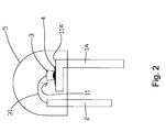
- Figure 2 is a schematic side elevational view of a light emitting diode constructed in accordance with a second embodiment of the present invention
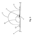
- Figure 3 is a schematic side elevational view of a light emitting diode constructed in accordance with a third embodiment of the present invention.
- Figure 4 is a schematic side elevational view of a conventional light emitting diode.
- a light emitting diode (LED) constructed in accordance with a first embodiment of the present invention comprises a first lead frame 1 and a second lead frame 2 spaced from each other and forming electrodes of different electrical polarities for the LED.
- a recess or cup 11 is formed on an upper end of the first lead frame 1 and receives an LED die 3 therein.
- a conductive wire 31 connects the die 3 to the second lead frame 2.
- An encapsulation 5 is formed and surrounds ends of the lead frames 1, 2 and the die 3.
- a phosphor layer 4 is formed on an inside surface of the cup 11 and is interposed between the die 3 and the cup 11.
- the phosphor layer 4 is comprised of a mixture of a die bonding adhesive and a solid-state luminance material.
- the die bonding adhesive may be conductive or non-conductive.
- An example is epoxy.
- the solid-state luminance material may comprise phosphor powders mixed in the die bonding adhesive.
- Light generated by the die 3 is partially projected onto the phosphor layer 4, stimulating the phosphor layer 4 to give off a second light, which may be different from the light from the die 3. The color of the second light is dependent upon the phosphor substance mixed in the phosphor layer 4.
- the die 3 may emit a blue light, while the phosphor layer 4 receives the blue light and in turn gives off a yellow light. Both the blue light and the yellow lights travel through the encapsulation 5 and project outward. The mixture of the blue and yellow lights gives a white light. Thus, the LED of the present invention may give off white light.
- the yellow light from the phosphor layer 4 may also be used to control the brightness of the final light projecting out of the encapsulation 5.
- Figure 2 shows a light emitting diode constructed in accordance with a second embodiment of the present invention, comprising a first lead frame 1A forming a support platform 11A having a flat surface (not labeled) on which a phosphor layer 4 is coated.
- the phosphor layer 4 is comprised of a die bonding adhesive and phosphor powders mixed together.
- An LED die 3 is attached to the phosphor layer 4 and is connected to a second lead frame 2 by a conductive wire 31.
- An encapsulation 5 is then formed around the die 3 and the phosphor layer 4.
- light emitted from the die 3 is partly projected onto the phosphor layer 4, which in turn gives off a second light that may be different from the light from the die 3.
- the phosphor layer 4 allows for control of brightness and color of the light eventually projecting out of the encapsulation 5 and a stable lighting may be obtained with the light emitting diode. As a consequence, mass production of quality-controlled light emitting diodes is made possible.
- Figure 3 shows a light emitting diode constructed in accordance with a third embodiment of the present invention, which is directly mounted to a circuit board 6.
- the light emitting diode of the third embodiment comprises a first conductive trace 61 and a second conductive trace 62 formed on the circuit board 6 and spaced from each other and connected to opposite electrical terminals of a power source.
- a phosphor layer 4 is coated on the first conductive trace 61.
- the phosphor layer 4 is comprised of a die bonding adhesive and phosphor powders mixed together.
- An LED die 3 is attached to the phosphor layer 4 and is connected to the second conductive trace 62 by a conductive wire 31.
- An encapsulation 5 is then formed around the die 3 and the phosphor layer 4.
- the phosphor layer 4 allows for control of brightness and color of the light eventually projecting out of the encapsulation 5 and a stable lighting may be obtained with the light emitting diode. As a consequence, mass production of quality-controlled light emitting diodes is made possible.
Landscapes
- Led Device Packages (AREA)
Priority Applications (1)
| Application Number | Priority Date | Filing Date | Title |
|---|---|---|---|
| EP03001046A EP1439585A1 (de) | 2003-01-17 | 2003-01-17 | Leuchtdiode mit dünnschicht Phosphor |
Applications Claiming Priority (1)
| Application Number | Priority Date | Filing Date | Title |
|---|---|---|---|
| EP03001046A EP1439585A1 (de) | 2003-01-17 | 2003-01-17 | Leuchtdiode mit dünnschicht Phosphor |
Publications (1)
| Publication Number | Publication Date |
|---|---|
| EP1439585A1 true EP1439585A1 (de) | 2004-07-21 |
Family
ID=32524157
Family Applications (1)
| Application Number | Title | Priority Date | Filing Date |
|---|---|---|---|
| EP03001046A Withdrawn EP1439585A1 (de) | 2003-01-17 | 2003-01-17 | Leuchtdiode mit dünnschicht Phosphor |
Country Status (1)
| Country | Link |
|---|---|
| EP (1) | EP1439585A1 (de) |
Cited By (2)
| Publication number | Priority date | Publication date | Assignee | Title |
|---|---|---|---|---|
| EP1770794A2 (de) | 2005-09-28 | 2007-04-04 | Osram Opto Semiconductors GmbH | Optoelektronische Halbleiterchip, Verfahren zu dessen Herstellung und optoelektronisches Bauteil |
| CN101752484B (zh) * | 2008-12-22 | 2012-05-16 | 富准精密工业(深圳)有限公司 | 发光二极管及其制造方法 |
Citations (4)
| Publication number | Priority date | Publication date | Assignee | Title |
|---|---|---|---|---|
| JPH1168166A (ja) * | 1997-08-19 | 1999-03-09 | Sanken Electric Co Ltd | 発光ダイオード装置 |
| EP1107321A1 (de) * | 1999-06-23 | 2001-06-13 | Citizen Electronics Co., Ltd. | Lichtemittierende diode |
| EP1187228A1 (de) * | 2000-02-09 | 2002-03-13 | Nippon Leiz Corporation | Lichtquelle |
| GB2373368A (en) * | 2001-03-12 | 2002-09-18 | Arima Optoelectronics Corp | White light emitting LED devices |
-
2003
- 2003-01-17 EP EP03001046A patent/EP1439585A1/de not_active Withdrawn
Patent Citations (4)
| Publication number | Priority date | Publication date | Assignee | Title |
|---|---|---|---|---|
| JPH1168166A (ja) * | 1997-08-19 | 1999-03-09 | Sanken Electric Co Ltd | 発光ダイオード装置 |
| EP1107321A1 (de) * | 1999-06-23 | 2001-06-13 | Citizen Electronics Co., Ltd. | Lichtemittierende diode |
| EP1187228A1 (de) * | 2000-02-09 | 2002-03-13 | Nippon Leiz Corporation | Lichtquelle |
| GB2373368A (en) * | 2001-03-12 | 2002-09-18 | Arima Optoelectronics Corp | White light emitting LED devices |
Non-Patent Citations (1)
| Title |
|---|
| PATENT ABSTRACTS OF JAPAN vol. 1999, no. 08 30 June 1999 (1999-06-30) * |
Cited By (5)
| Publication number | Priority date | Publication date | Assignee | Title |
|---|---|---|---|---|
| EP1770794A2 (de) | 2005-09-28 | 2007-04-04 | Osram Opto Semiconductors GmbH | Optoelektronische Halbleiterchip, Verfahren zu dessen Herstellung und optoelektronisches Bauteil |
| DE102005046450A1 (de) * | 2005-09-28 | 2007-04-05 | Osram Opto Semiconductors Gmbh | Optoelektronischer Halbleiterchip, Verfahren zu dessen Herstellung und optoelektronisches Bauteil |
| EP1770794A3 (de) * | 2005-09-28 | 2008-07-09 | OSRAM Opto Semiconductors GmbH | Optoelektronische Halbleiterchip, Verfahren zu dessen Herstellung und optoelektronisches Bauteil |
| US7838876B2 (en) | 2005-09-28 | 2010-11-23 | Osram Opto Semiconductors Gmbh | Optoelectronic semiconductor device in which current spreading layer of sol gel material mixed with nanoparticles is mixed with wavelength conversion dyes |
| CN101752484B (zh) * | 2008-12-22 | 2012-05-16 | 富准精密工业(深圳)有限公司 | 发光二极管及其制造方法 |
Similar Documents
| Publication | Publication Date | Title |
|---|---|---|
| US7956378B2 (en) | Light emitting diode package and method of manufacturing the same | |
| KR100586731B1 (ko) | 발광 다이오드와 전류구동형 집적회로를 구비하며 패키지화된 발광 반도체소자 | |
| JP2002076444A (ja) | 白色発光ダイオードの製造方法 | |
| JP4045710B2 (ja) | 半導体発光装置の製造方法 | |
| EP1107321A1 (de) | Lichtemittierende diode | |
| JP2001298216A (ja) | 表面実装型の半導体発光装置 | |
| JP2000349345A (ja) | 半導体発光装置 | |
| JP2003017753A (ja) | 発光装置 | |
| US20040135162A1 (en) | Light emitting diode | |
| JP2003168828A (ja) | 表面実装型発光ダイオード及びその製造方法 | |
| KR100348377B1 (ko) | 백색 발광 다이오드의 제조 방법 | |
| KR100550852B1 (ko) | 4 리드의 다색 발광 소자 | |
| WO2025098296A1 (zh) | 杯中杯双色温led | |
| JP2003077317A (ja) | Ledランプ | |
| US20020125494A1 (en) | Semiconductor light emitting device and method of producing the same | |
| CN2664204Y (zh) | 内置驱动集成电路芯片的发光半导体器件 | |
| JP2002151744A (ja) | 光源装置 | |
| CN100424872C (zh) | 白光发光二极管的光源构造 | |
| JP2002158376A (ja) | 発光ダイオード照明装置 | |
| US20080042157A1 (en) | Surface mount light emitting diode package | |
| CN115172343A (zh) | 一种rgb加白光的led灯珠及制作方法 | |
| KR100999712B1 (ko) | 발광 다이오드 패키지 | |
| KR101047795B1 (ko) | 반도체 발광소자 | |
| CN222071967U (zh) | Smd led灯珠 | |
| JP2012015558A (ja) | 発光ダイオードパッケージ及びその製造方法 |
Legal Events
| Date | Code | Title | Description |
|---|---|---|---|
| PUAI | Public reference made under article 153(3) epc to a published international application that has entered the european phase |
Free format text: ORIGINAL CODE: 0009012 |
|
| AK | Designated contracting states |
Kind code of ref document: A1 Designated state(s): AT BE BG CH CY CZ DE DK EE ES FI FR GB GR HU IE IT LI LU MC NL PT SE SI SK TR |
|
| AX | Request for extension of the european patent |
Extension state: AL LT LV MK RO |
|
| 17P | Request for examination filed |
Effective date: 20041227 |
|
| AKX | Designation fees paid |
Designated state(s): DE FR GB IE IT SE |
|
| 17Q | First examination report despatched |
Effective date: 20050404 |
|
| STAA | Information on the status of an ep patent application or granted ep patent |
Free format text: STATUS: THE APPLICATION IS DEEMED TO BE WITHDRAWN |
|
| 18D | Application deemed to be withdrawn |
Effective date: 20050815 |