EP1107321A1 - Lichtemittierende diode - Google Patents
Lichtemittierende diode Download PDFInfo
- Publication number
- EP1107321A1 EP1107321A1 EP00937311A EP00937311A EP1107321A1 EP 1107321 A1 EP1107321 A1 EP 1107321A1 EP 00937311 A EP00937311 A EP 00937311A EP 00937311 A EP00937311 A EP 00937311A EP 1107321 A1 EP1107321 A1 EP 1107321A1
- Authority
- EP
- European Patent Office
- Prior art keywords
- light emitting
- emitting diode
- fluorescent material
- material containing
- diode element
- Prior art date
- Legal status (The legal status is an assumption and is not a legal conclusion. Google has not performed a legal analysis and makes no representation as to the accuracy of the status listed.)
- Withdrawn
Links
Images


Classifications
-
- H—ELECTRICITY
- H10—SEMICONDUCTOR DEVICES; ELECTRIC SOLID-STATE DEVICES NOT OTHERWISE PROVIDED FOR
- H10H—INORGANIC LIGHT-EMITTING SEMICONDUCTOR DEVICES HAVING POTENTIAL BARRIERS
- H10H20/00—Individual inorganic light-emitting semiconductor devices having potential barriers, e.g. light-emitting diodes [LED]
- H10H20/80—Constructional details
- H10H20/85—Packages
- H10H20/851—Wavelength conversion means
- H10H20/8516—Wavelength conversion means having a non-uniform spatial arrangement or non-uniform concentration, e.g. patterned wavelength conversion layer or wavelength conversion layer with a concentration gradient
-
- H—ELECTRICITY
- H10—SEMICONDUCTOR DEVICES; ELECTRIC SOLID-STATE DEVICES NOT OTHERWISE PROVIDED FOR
- H10H—INORGANIC LIGHT-EMITTING SEMICONDUCTOR DEVICES HAVING POTENTIAL BARRIERS
- H10H20/00—Individual inorganic light-emitting semiconductor devices having potential barriers, e.g. light-emitting diodes [LED]
- H10H20/80—Constructional details
- H10H20/85—Packages
- H10H20/8506—Containers
-
- H—ELECTRICITY
- H10—SEMICONDUCTOR DEVICES; ELECTRIC SOLID-STATE DEVICES NOT OTHERWISE PROVIDED FOR
- H10W—GENERIC PACKAGES, INTERCONNECTIONS, CONNECTORS OR OTHER CONSTRUCTIONAL DETAILS OF DEVICES COVERED BY CLASS H10
- H10W72/00—Interconnections or connectors in packages
- H10W72/30—Die-attach connectors
-
- H—ELECTRICITY
- H10—SEMICONDUCTOR DEVICES; ELECTRIC SOLID-STATE DEVICES NOT OTHERWISE PROVIDED FOR
- H10W—GENERIC PACKAGES, INTERCONNECTIONS, CONNECTORS OR OTHER CONSTRUCTIONAL DETAILS OF DEVICES COVERED BY CLASS H10
- H10W72/00—Interconnections or connectors in packages
- H10W72/071—Connecting or disconnecting
- H10W72/073—Connecting or disconnecting of die-attach connectors
-
- H—ELECTRICITY
- H10—SEMICONDUCTOR DEVICES; ELECTRIC SOLID-STATE DEVICES NOT OTHERWISE PROVIDED FOR
- H10W—GENERIC PACKAGES, INTERCONNECTIONS, CONNECTORS OR OTHER CONSTRUCTIONAL DETAILS OF DEVICES COVERED BY CLASS H10
- H10W72/00—Interconnections or connectors in packages
- H10W72/071—Connecting or disconnecting
- H10W72/075—Connecting or disconnecting of bond wires
- H10W72/07541—Controlling the environment, e.g. atmosphere composition or temperature
- H10W72/07554—Controlling the environment, e.g. atmosphere composition or temperature changes in dispositions
-
- H—ELECTRICITY
- H10—SEMICONDUCTOR DEVICES; ELECTRIC SOLID-STATE DEVICES NOT OTHERWISE PROVIDED FOR
- H10W—GENERIC PACKAGES, INTERCONNECTIONS, CONNECTORS OR OTHER CONSTRUCTIONAL DETAILS OF DEVICES COVERED BY CLASS H10
- H10W72/00—Interconnections or connectors in packages
- H10W72/50—Bond wires
- H10W72/541—Dispositions of bond wires
- H10W72/547—Dispositions of multiple bond wires
-
- H—ELECTRICITY
- H10—SEMICONDUCTOR DEVICES; ELECTRIC SOLID-STATE DEVICES NOT OTHERWISE PROVIDED FOR
- H10W—GENERIC PACKAGES, INTERCONNECTIONS, CONNECTORS OR OTHER CONSTRUCTIONAL DETAILS OF DEVICES COVERED BY CLASS H10
- H10W72/00—Interconnections or connectors in packages
- H10W72/851—Dispositions of multiple connectors or interconnections
- H10W72/874—On different surfaces
- H10W72/884—Die-attach connectors and bond wires
-
- H—ELECTRICITY
- H10—SEMICONDUCTOR DEVICES; ELECTRIC SOLID-STATE DEVICES NOT OTHERWISE PROVIDED FOR
- H10W—GENERIC PACKAGES, INTERCONNECTIONS, CONNECTORS OR OTHER CONSTRUCTIONAL DETAILS OF DEVICES COVERED BY CLASS H10
- H10W74/00—Encapsulations, e.g. protective coatings
-
- H—ELECTRICITY
- H10—SEMICONDUCTOR DEVICES; ELECTRIC SOLID-STATE DEVICES NOT OTHERWISE PROVIDED FOR
- H10W—GENERIC PACKAGES, INTERCONNECTIONS, CONNECTORS OR OTHER CONSTRUCTIONAL DETAILS OF DEVICES COVERED BY CLASS H10
- H10W90/00—Package configurations
-
- H—ELECTRICITY
- H10—SEMICONDUCTOR DEVICES; ELECTRIC SOLID-STATE DEVICES NOT OTHERWISE PROVIDED FOR
- H10W—GENERIC PACKAGES, INTERCONNECTIONS, CONNECTORS OR OTHER CONSTRUCTIONAL DETAILS OF DEVICES COVERED BY CLASS H10
- H10W90/00—Package configurations
- H10W90/701—Package configurations characterised by the relative positions of pads or connectors relative to package parts
- H10W90/731—Package configurations characterised by the relative positions of pads or connectors relative to package parts of die-attach connectors
- H10W90/734—Package configurations characterised by the relative positions of pads or connectors relative to package parts of die-attach connectors between a chip and a stacked insulating package substrate, interposer or RDL
-
- H—ELECTRICITY
- H10—SEMICONDUCTOR DEVICES; ELECTRIC SOLID-STATE DEVICES NOT OTHERWISE PROVIDED FOR
- H10W—GENERIC PACKAGES, INTERCONNECTIONS, CONNECTORS OR OTHER CONSTRUCTIONAL DETAILS OF DEVICES COVERED BY CLASS H10
- H10W90/00—Package configurations
- H10W90/701—Package configurations characterised by the relative positions of pads or connectors relative to package parts
- H10W90/751—Package configurations characterised by the relative positions of pads or connectors relative to package parts of bond wires
- H10W90/754—Package configurations characterised by the relative positions of pads or connectors relative to package parts of bond wires between a chip and a stacked insulating package substrate, interposer or RDL
-
- H—ELECTRICITY
- H10—SEMICONDUCTOR DEVICES; ELECTRIC SOLID-STATE DEVICES NOT OTHERWISE PROVIDED FOR
- H10W—GENERIC PACKAGES, INTERCONNECTIONS, CONNECTORS OR OTHER CONSTRUCTIONAL DETAILS OF DEVICES COVERED BY CLASS H10
- H10W90/00—Package configurations
- H10W90/701—Package configurations characterised by the relative positions of pads or connectors relative to package parts
- H10W90/751—Package configurations characterised by the relative positions of pads or connectors relative to package parts of bond wires
- H10W90/756—Package configurations characterised by the relative positions of pads or connectors relative to package parts of bond wires between a chip and a stacked lead frame, conducting package substrate or heat sink
Definitions
- the present invention relates to a light emitting diode of wavelength conversion type, and more particularly to a type of light emitting diode which converts blue luminescence into white.
- the former one is a light emitting diode 1 of lead frame type, having a structure in which: a recess 3 is arranged in a metal stem 2, one of the lead frames; a light emitting diode element 4 made of gallium nitride type compound semiconductor is placed on and fixed to this recess 3; and this light emitting diode element 4 is connected with the aforementioned metal stem 2 and a metal post 5, the other lead frame, by using bonding wires 6 and 7, respectively; the whole being sealed by a transparent resin 9 of bombshell form.
- a fluorescent material 8 for wavelength conversion is dispersed into the transparent resin 9 mentioned above.
- the light emitting diode 1 When the light emitting diode 1 is lit, the light emitted from the light emitting diode element 4 impinges the fluorescent substance 8 and is converted into yellow so that it can blend with the original blue luminescence from the light emitting diode element 4 to present white in luminescent color.
- a light emitting diode element 4 for blue luminescence made of gallium nitride type compound semiconductor is placed on and fixed to a recess 3 in the above-mentioned metal stem 2, and a fluorescent material containing resin 8 is filled into the above-mentioned recess 3 so as to cover the top of this light emitting diode element 4. Accordingly, in the light emitting diode 1 having such a configuration, the blue luminescence emitted from the light emitting diode element 4 excites the fluorescent material in the fluorescent material containing resin 8, and the light converted thus in wavelength blends with the original blue luminescence from the light emitting diode element 4 to come out as white luminescence.
- the former had the problem that since the fluorescent material 8 is dispersed into the transparent resin 9 which seals the light emitting diode element 4, the light passing through the transparent resin 9 drops in transmittance, decreasing the intensity of the white luminescence. It also had the problem that the fluorescent material 8 is higher than the transparent resin 9 in specific gravity and thus is difficult to disperse uniformly, causing chromaticity variations not only between different light emitting diodes but also within a single light emitting diode.
- the latter had the problem that since the fluorescent material containing resin 8 covers the vicinity of the top of the light emitting diode element 4, the transmission of the light from the light emitting diode element 4 is hampered by the fluorescent material so that white luminescence of high intensity cannot be obtained.
- a light emitting diode according to the present invention comprises a light emitting diode element mounted on a base, the light emitting diode element being protected at its surface side by a resin seal member, the light emitting diode being characterized in that a fluorescent material containing layer is arranged on the back side of the aforesaid light emitting diode element.
- the fluorescent material containing layer is arranged on the back side of the light emitting diode element so that the light from the light emitting diode element is converted in waveform at the back side of the light emitting diode.
- a light emitting diode according to another aspect of the present invention is characterized in that the aforesaid light emitting diode element is a light emitting diode element made of gallium nitride type compound semiconductor or SiC type compound semiconductor.
- the fluorescent material containing layer is arranged on the back side of the blue-luminescence light emitting diode element formed of the above-mentioned compound, so that the light from the light emitting diode element is converted in wavelength at the back side of the light emitting diode element. Therefore, white luminescence of high luminescent intensity is obtained.
- a light emitting diode comprises two or more light emitting diode elements mounted on a base, the light emitting diode elements being protected at their surface side by a resin seal member, the light emitting diode being characterized in that: at least one of the aforesaid two or more light emitting diode elements is a light emitting diode element for blue luminescence, made of gallium nitride type compound semiconductor or SiC type compound semiconductor; and a fluorescent material containing layer is arranged on the back side of this light emitting diode element for blue luminescence.
- multicolor luminescence including white luminescence can be achieved by simple means.
- a light emitting diode is characterized in that: the aforesaid fluorescent material containing layer is composed of a fluorescent material dispersed into an adhesive; and the back of the light emitting diode element is firmly fixed to the base by the adhesive action of this fluorescent material containing layer.
- the dispersion of the fluorescent material into the adhesion makes it possible to arrange the fluorescent material simultaneously during the process of adhesive bonding the light emitting diode element.
- a light emitting diode is characterized in that; the aforesaid fluorescent material containing layer is formed with a fluorescent material and an adhesive separate from each other; and a fluorescent material containing resin layer and an adhesive layer are formed in layers on the top surface of the base.
- the fluorescent material and the adhesive are formed in separate layers on the base. This ensures a greater thickness of the fluorescent material content and facilitates thickness control as well, with the advantage that the degree of blending with blue luminescence is easy to adjust.
- a light emitting diode is characterized in that the aforesaid fluorescent material containing layer is formed on the top surface of the base by printing means.
- overprinting can be performed to secure a thickness of the fluorescent material containing layer and control the thickness as well.
- a light emitting diode is characterized in that the aforesaid fluorescent material containing layer is a fluorescent material containing resin sheet pasted on the top surface of the base.
- the thickness of the fluorescent material containing resin sheet can be appropriately adjusted so as to secure a thickness of the fluorescent material containing layer and control the thickness as described above.
- a light emitting diode is characterized in that the aforesaid fluorescent material is an yttrium compound.
- an yttrium compound for the fluorescent material allows efficient wavelength conversion from visible light of shorter wavelength into visible light of longer wavelength.
- a light emitting diode is characterized in that the periphery of the aforesaid fluorescent material containing layer is surrounded by a dam provided on the top surface of the aforesaid base.
- the dam surrounding the periphery of the fluorescent material containing layer by the dam makes it possible to ensure a predetermined thickness of the fluorescent material containing layer, as well as to secure a uniform thickness under the entire bottom surface of the light emitting diode element.
- a light emitting diode is characterized in that a reflecting surface is arranged on the bottom side of the aforesaid fluorescent material containing layer or the top surface of the base.
- a thin film layer of high reflectivity such as copper foil and aluminum foil, can be arranged on the bottom side of the fluorescent material containing layer so that the yellow luminescence converted in wavelength by the fluorescent material is reflected upward with efficiency.
- a light emitting diode is characterized in that an upward reflecting surface tilting outward is arranged around the aforesaid fluorescent material containing layer.
- the light emitted in all directions from the light emitting diode element are gathered upward by the reflecting surface, thereby achieving a further improvement in intensity.
- a light emitting diode according to another aspect of the present invention is characterized in that a lens portion of convex shape is formed on the top side of the aforesaid resin seal member.
- the lens portion of convex shape is formed on the top surface of the resin seal member, light traveling straight through the resin seal member is refracted upward at the interface surface, enhancing the upward light-gathering power.
- a light emitting diode is characterized in that: the aforesaid resin seal member is formed flat at the top side; and a fluorescent material containing layer is formed on the top side.
- the formation of the fluorescent material containing layer on the top side of the resin seal material allows color adjustment on the top side.
- a light emitting diode is characterized in that the aforesaid base is a glass epoxy substrate, a solid-molded substrate of liquid crystal polymer, or a sheet metal substrate.
- glass epoxy substrates, solid-molded substrates of liquid crystal polymer, and sheet metal substrates can be selected as the base of the light emitting diode.
- a light emitting diode according to another aspect of the present invention is characterized in that: the aforesaid light emitting diode element is connected to a pair of electrodes arranged on the base; and these electrodes are surface-mounted directly to print wires on a motherboard.
- Figs. 1 through 3 show an embodiment in the case of application to a surface mount type light emitting diode.
- the surface mount type light emitting diode 11 achieves the surface mounting in such a manner that a pair of topside electrodes 13, 14 (cathode electrode and anode electrode) are patterned with a rectangular glass epoxy substrate (hereinafter, referred to as glass epoxy substrate) 12 as the base, and underside electrodes integrally formed thereto are fixed to printed wires 16 and 17 on a motherboard 15 with solder 18.
- a light emitting diode element 20 is mounted on the topside center of the above-mentioned glass epoxy substrate 12, and is fixed to the glass epoxy substrate 12 with a fluorescent material containing layer 21 applied to its back side.
- This light emitting diode element 20 is a blue light emitting element made of gallium nitride type compound semiconductor. As shown in Fig. 3, it has a structure in which an n-type semiconductor 32 and a p-type semiconductor 24 are grown on the top surface of a sapphire substrate 22.
- the n-type semiconductor 23 and the p-type semiconductor 24 are provided with electrodes 25 and 26, and connected to the topside electrodes 13 and 14 arranged on the above-mentioned glass epoxy substrate 12 with bonding wires 27 and 28 for blue luminescence.
- the fluorescent material containing layer 21 arranged on the back side of the light emitting diode element 20 is composed of, as shown in Fig. 3, an appropriate amount of fluorescent material 30 uniformly dispersed into an adhesive 29 as a base. This is applied by print to the top surface of the glass epoxy substrate 12 with a predetermined thickness. With the light emitting diode element 20 placed thereon, the adhesive 29 is heat solidified to fix the back side of the light emitting diode element 20 to the top surface of the glass epoxy substrate 12. The firm adhesion obtained between the adhesive 29 and the glass epoxy substrate 12 prevents the fluorescent material containing layer 21 from coming off.
- a fluorescent material containing resin sheet composed of a fluorescent material kneaded into a resin material may be formed and this fluorescent material containing resin sheet may be pasted onto the top surface of the base as the fluorescent material containing layer.
- the above-mentioned fluorescent material 30 is excited by luminescence energy from the light emitting diode element 20 to convert visible light of short wavelength into visible light of long wavelength. It is made of, for example, fluorescent substances such as an yttrium compound.
- the blue light 31 emitted downward in particular impinges the fluorescent material 30 dispersed in the fluorescent material containing layer 21 to excite the fluorescent material 30 so that it is converted in wavelength into yellow light 32 and emitted in all directions.
- this yellow light 32 blends with the blue light 31 that is emitted upward and sideways from the above-mentioned light emitting diode element 20, so as to present white luminescence when the light emitting diode 11 is seen.
- a resin seal member 33 of rectangular solid shape through which the aforementioned blue light 31 and wavelength-converted yellow light 32 travel straight ahead. Since it is chiefly composed of an epoxy type transparent resin and has no fluorescent material dispersed therein as distinct from heretofore, this resin seal member 33 is favorable in light transmittance, consequently achieving an improvement in the intensity of the white luminescence blended. Moreover, in this embodiment, the fluorescent material 30 is dispersed into the adhesive 29. Therefore, in contrast to the conventional cases where fluorescent materials are dispersed into resin seal members, the fluorescent material 30 produces no deviation in dispersion so that variations in chromaticity is suppressed during light emission.
- the fluorescent material containing layer 21 is far off the top surface of the resin seal member 33 and is hidden in the back side of the light emitting diode element 20. This means a structure less prone to effect of ultraviolet rays.
- dispersing agents such as silicon dioxide may be mixed into the resin seal member 33 for more uniform luminescence.
- the reflection efficiency of the light emitted backward from the light emitting diode element 20 can also be improved by providing a thin film layer of high reflectivity such as copper foil and aluminum foil on the bottom side of the fluorescent material containing layer 21 described above, or by extending, as shown in Fig. 4, one topside electrode (cathode electrode) 13 to form a mounting surface 35 and fixing the light emitting diode element 20 onto this mounting surface 35 via the fluorescent material containing layer 21.
- Figs. 5 and 6 show the second embodiment of the present invention.
- a rectangular hole 37 somewhat smaller than the plane shape of the light emitting diode element 20 is formed in the mounting surface 35 extended from the above-described topside electrode 13.
- This rectangular hole 37 is filled with the above-described fluorescent material containing layer 21, and the light emitting diode element 20 is placed on and fixed to the same.
- the other configurations are identical to those of the first embodiment described above.
- the inner rim of the rectangular hole 37 functions as a dam 38 to prevent the fluorescent material containing layer 21 from flowing away.
- the dam 38 for ensuring a predetermined thickness is not limited to the mounting surface 35 which forms a part of the topside electrode 13 mentioned above.
- Figs. 7 and 8 show the third embodiment of the present invention.
- the resin seal member 36 for protecting the surface side of the light emitting diode element 20 is formed in a hemispherical shape, functioning as a lens portion of convex shape to enhance the upward light-gathering power. That is, light traveling straight through the resin seal member 36 is refracted upward at the interface surface so that the enhanced light-gathering power achieves an improvement in the intensity of white luminescence.
- Fig. 9 shows the fourth embodiment of the present invention.
- a cylindrical reflecting frame 40 is arranged at the topside center of glass epoxy substrate 12.
- a light emitting diode element 20 is placed therein, and the surface side of this light emitting diode element 20 is protected by a hemispherical resin seal member 36 as in the third embodiment described above.
- the reflecting frame 40 forms an upward reflecting surface of tapered shape, with an inner peripheral wall 41 tilting outward, so that the light emitted from the light emitting diode element 20 is reflected by the inner peripheral wall 41 for upward condensation.
- Fig. 9 shows the fourth embodiment of the present invention.
- a cylindrical reflecting frame 40 is arranged at the topside center of glass epoxy substrate 12.
- a light emitting diode element 20 is placed therein, and the surface side of this light emitting diode element 20 is protected by a hemispherical resin seal member 36 as in the third embodiment described above.
- the reflecting frame 40 forms an upward reflecting surface of tapered shape, with an inner peripheral wall
- the light emitting diode element 20 is fixed to the top surface of the glass epoxy substrate 12 through the medium of a fluorescent material containing layer 21 having a fluorescent material 30 dispersed into an adhesive 29.
- the fluorescent material containing layer 21 is arranged, the lower peripheral edge of the inner peripheral wall 41 of the reflecting frame 40 can make a dam to prevent the fluorescent material containing layer 21 from flowing away, so as to ensure a predetermined layer thickness.
- the light emitted backward from the light emitting diode element 20 excites the fluorescent material 30 dispersed in the fluorescent material containing layer 21, and the light that is converted in wavelength by this excitation is reflected by the inner peripheral wall 41 of the reflecting frame 40 for upward condensation.
- both the reflected light condensed by the reflecting frame 40 and the light that travels directly through the resin seal member 36 from the light emitting diode element 20 are further condensed upward at the interface surface of the resin seal member 36.
- white luminescence of higher intensity as compared with the above-described embodiment is obtained.
- the same reflecting frame 40 as described above may be provided in a resin seal member 33 of rectangular solid shape. In that case, the light gathering effect is obtained from the reflecting frame 40 alone.
- Figs. 11 and 12 show the fifth embodiment of the present invention.
- the light emitting diode 11 uses as its base a solid-molded substrate 45 molded of a liquid crystal polymer.
- a bowl-shaped cup portion 46 is formed in the center of the solid-molded substrate 45.
- a cathode and an anode, or topside electrodes, 13 and 14 are formed on the top surface of the solid-molded substrate 45 to the right and left astride a slit 47 in the center.
- On the inner periphery of the above-mentioned cup portion 46 are formed a reflecting surface 48 which is integrally molded with the topside electrodes 13 and 14 mentioned above.
- This reflecting surface 48 is hollowed round at the bottom 49 of the cup portion 46, so that the solid-molded substrate 45 is seen directly. Then, the same fluorescent material containing layer 21 as described above is applied to this bottom 49, and the light emitting diode element 20 is placed on and fixed to the same. Incidentally, a pair of electrodes of the light, emitting diode element 20 and the above-mentioned topside electrodes 13 and 14 are connected with each other using bonding wires 27 and 28. Even in this embodiment, when the fluorescent material containing layer 21 is arranged in this embodiment, the lower peripheral edge of the reflecting surface 48 makes a dam to prevent the fluorescent material containing layer 21 from flowing away, so as to ensure a predetermined layer thickness.
- the above-mentioned light emitting diode element 20 and the bonding wires 27 and 28 are protected by a transparent resin seal member 33 which is formed on the top side of the solid-molded substrate 45, including the cup portion 46.
- the thickness of the resin seal member 33 projecting to the top side of the solid-molded substrate 45 is suppressed, so that the light emitting diode 11 becomes low in profile as a whole.
- underside electrodes integrally molded with the above-mentioned topside electrodes 13 and 14 are formed on the bottom side of the solid-molded substrate 45.
- the light emitted backward from the light emitting diode element 20 excites the fluorescent material 30 dispersed in the fluorescent material containing layer 21.
- the light that is converted in wavelength by this excitation is reflected by the reflecting surface 48 of the cup portion 46 so that it travels upward to enhance the light-gathering power, presenting white luminescence of high intensity.
- Fig. 13 shows the sixth embodiment of the present invention.
- the light emitting diode 11 according to this embodiment uses a solid-molded substrate 45 as in the fifth embodiment described above, but differs in that the resin seal member 36 for sealing the surface side of the light emitting diode element 20 is formed in a hemispherical shape.
- the top of the resin seal member 36 can be positioned generally right above the light emitting diode element 20 to enhance the light-gathering power. Therefore, the light-gathering power from the resin seal member 36 can be expected in addition to the light-gathering effect by the reflecting surface 48 of the cup portion 46, whereby white luminescence of yet higher intensity can be obtained.
- Fig. 14 shows the seventh embodiment of the present invention.
- a fluorescent material containing layer 39 is formed thinly on the top side of a rectangular-solid-shaped resin seal member 33 so as to allow color adjustment on the top surface.
- the fluorescent material containing layer 39 is composed of a fluorescent material 30 of the above-mentioned yttrium type or a different fluorescent material, dispersed into an organic solvent. It may be printed as paint on the top surface of the resin seal member 33, or formed into a sheet and pasted.
- the fluorescent material containing layer 39 is formed thinly, which makes it possible to minimize a drop in light transmittance in the resin seal member 33.
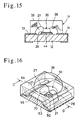
- Fig. 15 shows the eighth embodiment of the present invention.
- the adhesive 29 and the fluorescent material 30 are separated from each other.
- a fluorescent material containing resin 44 having the above-mentioned fluorescent material 30 dispersed into a transparent organic solvent is applied by print to the top surface of a glass epoxy substrate 12, and formed into a predetermined thickness through overprinting or the like.
- the fluorescent material containing resin 44 is dried before a transparent adhesive 29 is applied thereon to have a double-layer structure.
- a light emitting diode element 20 is placed on and fixed to the same.
- the blue luminescence emitted backward from the light emitting diode element 20 passes through the adhesive 29 and then impinges on the fluorescent material 30 dispersed in the fluorescent material containing resin 44 to excite the fluorescent material 30, so that it is converted in wavelength into yellow luminescence and emitted in all directions.
- the fluorescent material containing resin 44 is capable of securing a greater thickness and is easy to adjust in thickness, there is a merit that the degree of blend with blue luminescence is easily adjustable.
- it can also be formed by pasting a fluorescent material containing sheet.
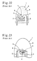
- Figs. 16 and 17 show the ninth embodiment of the present invention, in which a sheet metal substrate 50 pressed into a predetermined shape is used as the base, instead of the glass epoxy substrate 12 described above.
- This sheet metal substrate 50 is made of a material of favorable thermal conductivity, such as copper, iron, or phosphorus bronze.
- a cup portion 51 of bowl shape is press-formed in the center.
- the bottom surface 52 of the cup portion 51 is provided with a fluorescent material containing layer 21 having a fluorescent material 30 dispersed into an adhesive 29, onto which is fixed a light emitting diode element 20.
- the fluorescent material containing layer 21 is applied directly onto the sheet metal substrate 50, an insulating property is required of the adhesive 29.
- epoxy resin 53 is filled into the recesses at the back side of the sheet metal substrate 50 in order to secure the rigidity of the substrate.
- a splitting slit 54 is formed in one end of the sheet metal substrate 50 so that the right and left splits of the sheet metal substrate 50 themselves form a pair of topside electrodes.
- the inner peripheral wall of the above-mentioned cup portion 51 forms a reflecting surface 55 of tapered shape, and is combined with a hemispherical resin seal member 36 for sealing the surface side of the light emitting diode element 20 to enhance the light-gathering power.
- the lower peripheral edge of the reflecting surface 55 functions as a dam for securing the thickness of the fluorescent material containing layer 21.
- the light emitting diode 11 using the sheet metal substrate 50 may also be provided with a resin seal member 33 of rectangular solid shape with a flat top surface, as shown in Fig. 18. In this case, the splitting slit 54 is stopped by an insulating tape 56.
- Fig. 19 shows the tenth embodiment of the present invention.
- This embodiment of application to a multicolor light emitting diode 11a has a structure in which cathode electrodes 13a, 13b and anode electrodes 14a, 14b are patterned in right and left rows on the top surface of a rectangular glass epoxy substrate 12 to be the base, and the underside electrodes pass around behind via their respective through holes 19.
- a first light emitting diode element 20a and a second light emitting diode element 20b are mounted on the pair of cathode electrodes 13a and 13b formed on the top surface of the above-mentioned glass epoxy substrate 12, respectively.
- the first light emitting diode element 20a is a blue light emitting element made of the gallium nitride type compound semiconductor described above, and is connected to the above-mentioned cathode electrode 13a and anode electrode 14a with bonding wires 27 and 28.
- the first light emitting diode element 20a is adhesive bonded to the top surface of the cathode electrode 13a via a fluorescent material containing layer 21 arranged on its back side.
- This fluorescent material containing layer 21, as described above, is composed of an insulative adhesive as the base and an appropriate amount of fluorescent material uniformly dispersed into the same. This is applied to the top surface of the cathode electrode 13a with a predetermined thickness. With the light emitting diode element 20a placed thereon, the adhesive is heat solidified to fix the back surface of the first light emitting diode element 20a to the top surface of the cathode electrode 13a.
- the second light emitting diode element 20b is a red light emitting diode element made of a gallium aluminum indium phosphide type compound semiconductor (GaAlInP). It is fixed onto the cathode electrode 13b via a conductive adhesive 43 and is connected to the anode electrode 14b with a bonding wire 28.
- GaAlInP gallium aluminum indium phosphide type compound semiconductor
- This resin seal member 33 is composed chiefly of epoxy resin, and formed in a rectangular solid shape over the top side of the glass epoxy substrate 12 except the individual through holes 19 in the above-described cathode electrodes 13a, 13b and anode electrode 14a, 14b.
- the current flow through the first light emitting diode element 20a produces, as shown in Fig. 3 cited before, blue luminescence at the interface surface between the n-type semiconductor 23 and the p-type semiconductor 24.
- This blue luminescence is emitted upward, sideways, and downward as blue light 31.
- the blue light 31 emitted downward excites the fluorescent material 30 dispersed into the fluorescent material containing layer 21, undergoes wavelength conversion, and is emitted in all directions as yellow light 32.
- this yellow light 32 blends with the blue light 31 emitted upward and sideways from the above-mentioned first light emitting diode element 20a so as to be recognized as white luminescence when the multicolor light emitting diode lla is seen.
- the surface side of the first light emitting diode element 20a is protected by the resin seal member 33 of rectangular solid shape, through which the aforementioned blue light 31 and wavelength-converted yellow light 32 travel straight ahead. Since it is chiefly composed of an epoxy type transparent resin and includes no fluorescent material as distinct from heretofore, this resin seal member 33 is favorable in light transmittance, consequently achieving an improvement in the intensity of the white luminescence.
- white luminescence can be obtained simply by passing a current through the first light emitting diode element 20a. This means significantly lower current consumption as compared with the conventional cases where a plurality of lights emitted from light emitting diode elements are blended to obtain white luminescence.
- red luminescence can be obtained by passing a current through the second light emitting diode element 20b. Since the resin seal member 33 is transparent, red luminescence of high intensity can be obtained without any drop in light transmittance.
- Fig. 20 shows the eleventh embodiment of the present invention, in which the second light emitting diode element 20b for red luminescence in the foregoing embodiment is replaced by one for blue luminescence and is placed on the cathode electrode 13b.
- This blue light emitting diode element 20b is made of the same gallium nitride type compound semiconductor as the first light emitting diode element 20a. It'is thus fixed on the top surface of the cathode electrode 13b via an insulative adhesive 42 and is put into conduction with the cathode electrode 13b and the anode electrode 14b by bonding wires 27 and 28, respectively.
- the other configurations are identical to those of the tenth embodiment described above, detailed description thereof will be omitted.
- the first light emitting diode element 20a presents white luminescence as in the foregoing embodiment, whereas the second light emitting diode element 20b produces blue luminescence when a current is supplied thereto. In this way, blue and white, two-color luminescence can be easily obtained despite the mounting of the precisely identical light emitting diode elements.
- Fig. 21 shows the twelfth embodiment of the present invention.
- the multicolor light emitting diode according to this embodiment is of full color and, as distinct from heretofore, can produce every color with its four light emitting diode elements. That is, in this configuration, white luminescence is emitted by a first light emitting diode element 20a, and all the colors other than white are displayed by combinations of second, third, and fourth light emitting diode elements 20b, 20c, and 20d.
- Cathode electrodes 13a-13d and anode electrodes 14a-14d are formed in four rows on an oblong glass epoxy substrate 12, and the first through fourth light emitting diode elements 20a-20d are mounted on the cathode electrodes 13a-13d in succession.
- the first through fourth light emitting diode elements 20a, 20b, 20c, and 20d are light emitting diode elements for white, green, blue, and red, respectively.
- the first to third light emitting diodes 20a, 20b, and 20c each are made of gallium nitride type compound semiconductor.
- the fourth light emitting diode element 20d is made of a gallium aluminum indium phosphide type compound semiconductor.
- the first light emitting diode 20a mentioned above is fixed to the top surface of the cathode electrode 13a with a fluorescent material containing layer 21.
- the second and third light emitting diode elements 20b and 20d are fixed to the top surfaces of the cathode electrodes 13b and 13c with an insulative adhesive 42.
- the fourth light emitting diode element 20d is fixed to the top surface of the cathode electrode 13d with a conductive adhesive 43.
- the first to third light emitting diode elements 20a, 20b, and 20c are connected to the respective cathode electrodes 13a, 13b, and 13c by bonding wires 27.
- Including the fourth light emitting diode element 20d they are connected to the anode electrodes 14a, 14b, 14c, and 14d by bonding wires 28.
- Above the first through fourth light emitting diode elements 20a-20d is provided a protection by an integrally-formed resin seal member 33 of rectangular solid shape.
- the individual light emitting diode elements 20a, 20b, 20c, and 20d not only can emit monochromatic luminescence, but the values of the currents to the second through fourth light emitting diode elements 20b, 20c, and 20d for green, blue, and red luminescence can be controlled to produce luminescence of any color as well.
- white luminescence can be obtained by making the first light emitting diode element 20a emit monochromatic luminescence. This eliminates the need for delicate current control as in conventional full-color light emitting diodes.
- the light emitting diodes of this invention may also be applied to the lead-frame types described in the conventional examples. That is, an adhesive that contains a fluorescent material can be applied to recesses in the metal stems to mount light emitting diode elements on, and light emitting diode elements made of gallium nitride type compound semiconductor can be fixed onto the same so that white luminescence of high intensity is obtained without the fluorescent material being dispersed into resin seal members of bombshell form.
- a light emitting diode according to the present invention can present white luminescence of high intensity, and thus is useful as a white light source in various types of display units or in optical communication.
- a light emitting diode according to the present invention is useful as a multicolor light emitting diode that is low in current consumption and easy of current control.
Landscapes
- Led Device Packages (AREA)
Applications Claiming Priority (7)
| Application Number | Priority Date | Filing Date | Title |
|---|---|---|---|
| JP17635099A JP3393089B2 (ja) | 1999-06-23 | 1999-06-23 | 発光ダイオード |
| JP17635099 | 1999-06-23 | ||
| JP19344199 | 1999-07-07 | ||
| JP19344199A JP3400958B2 (ja) | 1999-07-07 | 1999-07-07 | 多色発光ダイオード |
| JP20462399 | 1999-07-19 | ||
| JP20462399A JP3492945B2 (ja) | 1999-07-19 | 1999-07-19 | 発光ダイオード |
| PCT/JP2000/004006 WO2000079605A1 (fr) | 1999-06-23 | 2000-06-20 | Diode électroluminescente |
Publications (2)
| Publication Number | Publication Date |
|---|---|
| EP1107321A1 true EP1107321A1 (de) | 2001-06-13 |
| EP1107321A4 EP1107321A4 (de) | 2006-08-30 |
Family
ID=27324245
Family Applications (1)
| Application Number | Title | Priority Date | Filing Date |
|---|---|---|---|
| EP00937311A Withdrawn EP1107321A4 (de) | 1999-06-23 | 2000-06-20 | Lichtemittierende diode |
Country Status (5)
| Country | Link |
|---|---|
| US (1) | US6914267B2 (de) |
| EP (1) | EP1107321A4 (de) |
| KR (1) | KR100425566B1 (de) |
| CN (1) | CN1224112C (de) |
| WO (1) | WO2000079605A1 (de) |
Cited By (15)
| Publication number | Priority date | Publication date | Assignee | Title |
|---|---|---|---|---|
| GB2373368A (en) * | 2001-03-12 | 2002-09-18 | Arima Optoelectronics Corp | White light emitting LED devices |
| WO2003028103A3 (en) * | 2001-09-25 | 2003-12-18 | Intel Corp | Multi-stack surface mount light emitting diodes |
| EP1439585A1 (de) * | 2003-01-17 | 2004-07-21 | Unity Opto Technology Co., Ltd. | Leuchtdiode mit dünnschicht Phosphor |
| DE10261365A1 (de) * | 2002-12-30 | 2004-07-22 | Osram Opto Semiconductors Gmbh | Optoelektronisches Bauelement mit einer Mehrzahl von strahlungsemittierenden Halbleiterchips |
| EP1548850A4 (de) * | 2002-09-30 | 2005-12-21 | Toyoda Gosei Kk | Weisses licht emittierendes bauelement |
| WO2006076940A1 (de) * | 2005-01-18 | 2006-07-27 | Vishay Semiconductor Gmbh | Infrarot-transceiver und herstellungsverfahren |
| EP1187228A4 (de) * | 2000-02-09 | 2007-03-07 | Nippon Leiz Corp | Lichtquelle |
| EP1548851A3 (de) * | 2003-12-26 | 2009-02-18 | Stanley Electric Co., Ltd. | Lichtemittierende Halbleitervorrichtung mit Materialen zur wellenlängeumwandlung und dessen Herstellungsverfahhren |
| EP1453109A3 (de) * | 2003-02-28 | 2009-05-27 | Noritsu Koki Co., Ltd. | Lichtquelleneinheit aus Leuchtdioden |
| EP2711993A1 (de) * | 2012-09-25 | 2014-03-26 | Toshiba Lighting & Technology Corporation | Lichtemittierende Vorrichtung und Beleuchtungsvorrichtung |
| EP2506317A4 (de) * | 2009-11-27 | 2014-08-20 | Kyocera Corp | Lichtemittierende vorrichtung |
| EP1766693B1 (de) * | 2004-05-13 | 2017-09-27 | Seoul Semiconductor Co., Ltd. | Lichtemittierendes bauelement mit rgb-leuchtdioden und leuchtstoff |
| EP3270426A1 (de) * | 2009-12-22 | 2018-01-17 | Kabushiki Kaisha Toshiba | Lichtemittierende vorrichtung |
| EP1878052B1 (de) * | 2005-04-29 | 2018-12-26 | Lumileds Holding B.V. | Lichtemittierende diodenstruktur |
| WO2021216645A1 (en) * | 2020-04-21 | 2021-10-28 | H2Vr Holdco, Inc. | Surface mount device containing a plurality of pixels and sub-pixels |
Families Citing this family (135)
| Publication number | Priority date | Publication date | Assignee | Title |
|---|---|---|---|---|
| JP2001326390A (ja) * | 2000-05-18 | 2001-11-22 | Rohm Co Ltd | 裏面発光チップ型発光素子およびそれに用いる絶縁性基板 |
| DE10122002A1 (de) * | 2001-05-07 | 2002-11-21 | Osram Opto Semiconductors Gmbh | Gehäuse für ein optoelektronisches Bauelement und optoelektronisches Bauelement |
| US7936338B2 (en) | 2002-10-01 | 2011-05-03 | Sony Corporation | Display unit and its manufacturing method |
| JP2004128273A (ja) * | 2002-10-03 | 2004-04-22 | Sharp Corp | 発光素子 |
| CN100502062C (zh) * | 2003-04-30 | 2009-06-17 | 美商克立股份有限公司 | 具有小型光学元件的高功率发光器封装 |
| US7005679B2 (en) | 2003-05-01 | 2006-02-28 | Cree, Inc. | Multiple component solid state white light |
| US6803607B1 (en) * | 2003-06-13 | 2004-10-12 | Cotco Holdings Limited | Surface mountable light emitting device |
| WO2005124877A2 (en) * | 2004-06-18 | 2005-12-29 | Philips Intellectual Property & Standards Gmbh | Led with improve light emittance profile |
| US7534633B2 (en) * | 2004-07-02 | 2009-05-19 | Cree, Inc. | LED with substrate modifications for enhanced light extraction and method of making same |
| CN100449801C (zh) * | 2004-09-30 | 2009-01-07 | 晶元光电股份有限公司 | 半导体发光元件组成 |
| US7344902B2 (en) * | 2004-11-15 | 2008-03-18 | Philips Lumileds Lighting Company, Llc | Overmolded lens over LED die |
| US8125137B2 (en) * | 2005-01-10 | 2012-02-28 | Cree, Inc. | Multi-chip light emitting device lamps for providing high-CRI warm white light and light fixtures including the same |
| US7564180B2 (en) * | 2005-01-10 | 2009-07-21 | Cree, Inc. | Light emission device and method utilizing multiple emitters and multiple phosphors |
| TW201403859A (zh) | 2005-02-18 | 2014-01-16 | 日亞化學工業股份有限公司 | 具備控制配光特性用之透鏡之發光裝置 |
| US7205656B2 (en) * | 2005-02-22 | 2007-04-17 | Micron Technology, Inc. | Stacked device package for peripheral and center device pad layout device |
| CN100477302C (zh) * | 2005-02-23 | 2009-04-08 | 李洲科技股份有限公司 | 多波长发光二极体及其发光晶片构造 |
| KR100663906B1 (ko) * | 2005-03-14 | 2007-01-02 | 서울반도체 주식회사 | 발광 장치 |
| TWD114618S1 (zh) * | 2005-03-31 | 2006-12-21 | 首爾半導體股份有限公司 | 發光二極體 |
| US7514769B1 (en) * | 2005-08-13 | 2009-04-07 | National Semiconductor Corporation | Micro surface mount die package and method |
| EP1925037A4 (de) * | 2005-09-13 | 2011-10-26 | Showa Denko Kk | Lichtemittierende einrichtung |
| WO2007061789A1 (en) * | 2005-11-18 | 2007-05-31 | Cree, Inc. | Tile for solid state lighting panel |
| JP2007165811A (ja) * | 2005-12-16 | 2007-06-28 | Nichia Chem Ind Ltd | 発光装置 |
| EP1963740A4 (de) | 2005-12-21 | 2009-04-29 | Cree Led Lighting Solutions | Beleuchtungsvorrichtung und beleuchtungsverfahren |
| US7213940B1 (en) | 2005-12-21 | 2007-05-08 | Led Lighting Fixtures, Inc. | Lighting device and lighting method |
| TWI421438B (zh) | 2005-12-21 | 2014-01-01 | 克里公司 | 照明裝置 |
| KR20090009772A (ko) | 2005-12-22 | 2009-01-23 | 크리 엘이디 라이팅 솔루션즈, 인크. | 조명 장치 |
| KR100715457B1 (ko) | 2005-12-30 | 2007-05-07 | 서울반도체 주식회사 | 발광 다이오드 실장용 인쇄회로기판 제조방법 및 발광다이오드 패키지 |
| CN100459193C (zh) * | 2006-02-23 | 2009-02-04 | 亿光电子工业股份有限公司 | 白光发光二极管封装结构 |
| KR101144557B1 (ko) * | 2006-03-27 | 2012-05-11 | 엘지이노텍 주식회사 | 발광 다이오드 조명장치 및 그 제조방법 |
| US8998444B2 (en) * | 2006-04-18 | 2015-04-07 | Cree, Inc. | Solid state lighting devices including light mixtures |
| US9084328B2 (en) * | 2006-12-01 | 2015-07-14 | Cree, Inc. | Lighting device and lighting method |
| US9921428B2 (en) | 2006-04-18 | 2018-03-20 | Cree, Inc. | Light devices, display devices, backlighting devices, edge-lighting devices, combination backlighting and edge-lighting devices |
| US7821194B2 (en) * | 2006-04-18 | 2010-10-26 | Cree, Inc. | Solid state lighting devices including light mixtures |
| TWI460880B (zh) * | 2006-04-18 | 2014-11-11 | Cree Inc | 照明裝置及照明方法 |
| US8513875B2 (en) * | 2006-04-18 | 2013-08-20 | Cree, Inc. | Lighting device and lighting method |
| EP2008019B1 (de) | 2006-04-20 | 2015-08-05 | Cree, Inc. | Beleuchtungsvorrichtung und beleuchtungsverfahren |
| US7655957B2 (en) | 2006-04-27 | 2010-02-02 | Cree, Inc. | Submounts for semiconductor light emitting device packages and semiconductor light emitting device packages including the same |
| WO2007142947A2 (en) | 2006-05-31 | 2007-12-13 | Cree Led Lighting Solutions, Inc. | Lighting device with color control, and method of lighting |
| CN101589268A (zh) | 2006-05-31 | 2009-11-25 | 科锐Led照明科技公司 | 照明装置和照明方法 |
| TWI302043B (en) * | 2006-06-27 | 2008-10-11 | Everlight Electronics Co Ltd | Base structure for ultra-thin light-emitting diode and manufacturing method thereof |
| EP2060155A2 (de) * | 2006-08-23 | 2009-05-20 | Cree Led Lighting Solutions, Inc. | Beleuchtungsvorrichtung und beleuchtungsverfahren |
| JP4905009B2 (ja) * | 2006-09-12 | 2012-03-28 | 豊田合成株式会社 | 発光装置の製造方法 |
| KR101241528B1 (ko) | 2006-09-25 | 2013-03-08 | 엘지이노텍 주식회사 | 발광 장치 |
| CN101558501B (zh) | 2006-10-12 | 2015-04-22 | 科锐公司 | 照明装置及其制造方法 |
| US8029155B2 (en) * | 2006-11-07 | 2011-10-04 | Cree, Inc. | Lighting device and lighting method |
| EP2087563B1 (de) | 2006-11-15 | 2014-09-24 | The Regents of The University of California | Leuchtdiode mit strukturierter leuchtstoff-umwandlungsschicht |
| JP5372766B2 (ja) * | 2006-11-15 | 2013-12-18 | ザ リージェンツ オブ ザ ユニバーシティ オブ カリフォルニア | 光取り出し効率の高い球形led |
| US20090121250A1 (en) * | 2006-11-15 | 2009-05-14 | Denbaars Steven P | High light extraction efficiency light emitting diode (led) using glass packaging |
| JP5171841B2 (ja) * | 2006-11-30 | 2013-03-27 | クリー インコーポレイテッド | 照明デバイス及び照明方法 |
| US9441793B2 (en) * | 2006-12-01 | 2016-09-13 | Cree, Inc. | High efficiency lighting device including one or more solid state light emitters, and method of lighting |
| CN101611259B (zh) * | 2006-12-07 | 2012-06-27 | 科锐公司 | 照明装置和照明方法 |
| JP2010512662A (ja) | 2006-12-11 | 2010-04-22 | ザ リージェンツ オブ ザ ユニバーシティ オブ カリフォルニア | 透明発光ダイオード |
| WO2008073435A1 (en) * | 2006-12-11 | 2008-06-19 | The Regents Of The University Of California | Lead frame for transparent and mirrorless light emitting diode |
| TWI325186B (en) * | 2007-01-19 | 2010-05-21 | Harvatek Corp | Led chip package structure using ceramic material as a substrate |
| TW200834968A (en) * | 2007-02-13 | 2008-08-16 | Harvatek Corp | Method of making light-emitting diode structure with high heat dissipation effect and structure made thereby |
| JP5476128B2 (ja) * | 2007-02-22 | 2014-04-23 | クリー インコーポレイテッド | 照明装置、照明方法、光フィルタ、および光をフィルタリングする方法 |
| JP5089212B2 (ja) * | 2007-03-23 | 2012-12-05 | シャープ株式会社 | 発光装置およびそれを用いたledランプ、発光装置の製造方法 |
| US20080246397A1 (en) * | 2007-04-04 | 2008-10-09 | Bily Wang | Manufacturing method of white light led and structure thereof |
| CN101755164B (zh) * | 2007-05-08 | 2013-03-27 | 科锐公司 | 照明装置和照明方法 |
| US7901107B2 (en) * | 2007-05-08 | 2011-03-08 | Cree, Inc. | Lighting device and lighting method |
| US7744243B2 (en) * | 2007-05-08 | 2010-06-29 | Cree Led Lighting Solutions, Inc. | Lighting device and lighting method |
| EP2156090B1 (de) * | 2007-05-08 | 2016-07-06 | Cree, Inc. | Beleuchtungsvorrichtung und beleuchtungsverfahren |
| CN101711325B (zh) | 2007-05-08 | 2013-07-10 | 科锐公司 | 照明装置和照明方法 |
| US8208266B2 (en) * | 2007-05-29 | 2012-06-26 | Avx Corporation | Shaped integrated passives |
| USD576574S1 (en) * | 2007-07-17 | 2008-09-09 | Rohm Co., Ltd. | Light emitting diode module |
| US7863635B2 (en) | 2007-08-07 | 2011-01-04 | Cree, Inc. | Semiconductor light emitting devices with applied wavelength conversion materials |
| KR101283054B1 (ko) | 2007-08-20 | 2013-07-05 | 엘지이노텍 주식회사 | 발광 소자 |
| US11114594B2 (en) | 2007-08-24 | 2021-09-07 | Creeled, Inc. | Light emitting device packages using light scattering particles of different size |
| US8033684B2 (en) * | 2007-08-31 | 2011-10-11 | The Boeing Company | Starry sky lighting panels |
| US7857484B2 (en) * | 2007-08-31 | 2010-12-28 | The Boeing Company | Lighting panels including embedded illumination devices and methods of making such panels |
| CN101821544B (zh) * | 2007-10-10 | 2012-11-28 | 科锐公司 | 照明装置及制造方法 |
| US9634191B2 (en) * | 2007-11-14 | 2017-04-25 | Cree, Inc. | Wire bond free wafer level LED |
| US8866410B2 (en) | 2007-11-28 | 2014-10-21 | Cree, Inc. | Solid state lighting devices and methods of manufacturing the same |
| DE102007059133B4 (de) * | 2007-12-07 | 2023-04-06 | OSRAM Opto Semiconductors Gesellschaft mit beschränkter Haftung | Substrat für ein LED-Submount, LED-Submount und LED-Lichtquelle |
| US9431589B2 (en) * | 2007-12-14 | 2016-08-30 | Cree, Inc. | Textured encapsulant surface in LED packages |
| CN101939852A (zh) * | 2007-12-24 | 2011-01-05 | 三星Led株式会社 | 发光二极管封装件 |
| TWI422058B (zh) * | 2008-03-04 | 2014-01-01 | 億光電子工業股份有限公司 | 發光二極體封裝結構與其製造方法 |
| US8916890B2 (en) * | 2008-03-19 | 2014-12-23 | Cree, Inc. | Light emitting diodes with light filters |
| US8350461B2 (en) | 2008-03-28 | 2013-01-08 | Cree, Inc. | Apparatus and methods for combining light emitters |
| EP2158618A1 (de) * | 2008-05-20 | 2010-03-03 | Panasonic Corporation | Halbleiter-leuchtanordnung sowie lichtquellenanordnung und beleuchtungssystem damit |
| US8240875B2 (en) | 2008-06-25 | 2012-08-14 | Cree, Inc. | Solid state linear array modules for general illumination |
| JP5217800B2 (ja) | 2008-09-03 | 2013-06-19 | 日亜化学工業株式会社 | 発光装置、樹脂パッケージ、樹脂成形体並びにこれらの製造方法 |
| US8247827B2 (en) * | 2008-09-30 | 2012-08-21 | Bridgelux, Inc. | LED phosphor deposition |
| US8333631B2 (en) * | 2009-02-19 | 2012-12-18 | Cree, Inc. | Methods for combining light emitting devices in a package and packages including combined light emitting devices |
| US7967652B2 (en) | 2009-02-19 | 2011-06-28 | Cree, Inc. | Methods for combining light emitting devices in a package and packages including combined light emitting devices |
| JP2010245481A (ja) * | 2009-04-10 | 2010-10-28 | Sharp Corp | 発光装置 |
| US8089075B2 (en) * | 2009-04-17 | 2012-01-03 | Avago Technologies Ecbu Ip (Singapore) Pte. Ltd. | LFCC package with a reflector cup surrounded by a single encapsulant |
| US8101955B2 (en) * | 2009-04-17 | 2012-01-24 | Avago Technologies Ecbu Ip (Singapore) Pte. Ltd. | PLCC package with a reflector cup surrounded by an encapsulant |
| US20100270580A1 (en) * | 2009-04-22 | 2010-10-28 | Jason Loomis Posselt | Substrate based light source package with electrical leads |
| US9269875B2 (en) * | 2009-05-20 | 2016-02-23 | Intellectual Discovery Co., Ltd. | Light emitter |
| US8921876B2 (en) | 2009-06-02 | 2014-12-30 | Cree, Inc. | Lighting devices with discrete lumiphor-bearing regions within or on a surface of remote elements |
| USD623151S1 (en) * | 2009-06-05 | 2010-09-07 | Foxsemicon Integrated Technology, Inc. | Led lens |
| USD623152S1 (en) * | 2009-06-05 | 2010-09-07 | Foxsemicon Integrated Technology, Inc. | Led lens |
| US8339028B2 (en) * | 2009-06-30 | 2012-12-25 | Apple Inc. | Multicolor light emitting diodes |
| US8648546B2 (en) * | 2009-08-14 | 2014-02-11 | Cree, Inc. | High efficiency lighting device including one or more saturated light emitters, and method of lighting |
| US20110049539A1 (en) * | 2009-08-27 | 2011-03-03 | High Power Lighting Corporation | Light-Emitting Diode With High Color-Rendering Index |
| US8901845B2 (en) | 2009-09-24 | 2014-12-02 | Cree, Inc. | Temperature responsive control for lighting apparatus including light emitting devices providing different chromaticities and related methods |
| KR20120094477A (ko) | 2009-09-25 | 2012-08-24 | 크리, 인코포레이티드 | 낮은 눈부심 및 높은 광도 균일성을 갖는 조명 장치 |
| DE102009047789A1 (de) * | 2009-09-30 | 2011-03-31 | Osram Gesellschaft mit beschränkter Haftung | Mischlichtquelle |
| KR101034054B1 (ko) * | 2009-10-22 | 2011-05-12 | 엘지이노텍 주식회사 | 발광소자 패키지 및 그 제조방법 |
| US9435493B2 (en) | 2009-10-27 | 2016-09-06 | Cree, Inc. | Hybrid reflector system for lighting device |
| CN101707233A (zh) * | 2009-11-05 | 2010-05-12 | 绍兴晶彩光电技术有限公司 | 一种发光二极管及其制造方法 |
| US8508116B2 (en) | 2010-01-27 | 2013-08-13 | Cree, Inc. | Lighting device with multi-chip light emitters, solid state light emitter support members and lighting elements |
| US9275979B2 (en) | 2010-03-03 | 2016-03-01 | Cree, Inc. | Enhanced color rendering index emitter through phosphor separation |
| JP2011204897A (ja) * | 2010-03-25 | 2011-10-13 | Toshiba Lighting & Technology Corp | 発光モジュール |
| US8329482B2 (en) | 2010-04-30 | 2012-12-11 | Cree, Inc. | White-emitting LED chips and method for making same |
| JP5528900B2 (ja) * | 2010-04-30 | 2014-06-25 | ローム株式会社 | 発光素子モジュール |
| WO2011143197A2 (en) | 2010-05-13 | 2011-11-17 | Cree, Inc. | Lighting device and method of making |
| US8684559B2 (en) | 2010-06-04 | 2014-04-01 | Cree, Inc. | Solid state light source emitting warm light with high CRI |
| MY152737A (en) * | 2010-08-24 | 2014-11-28 | Silq Malaysia Sdn Bhd | Methodology of forming optical lens for semiconductor light emitting device |
| JP5864089B2 (ja) * | 2010-08-25 | 2016-02-17 | 日亜化学工業株式会社 | 発光装置の製造方法 |
| US8556469B2 (en) | 2010-12-06 | 2013-10-15 | Cree, Inc. | High efficiency total internal reflection optic for solid state lighting luminaires |
| CN102569594A (zh) * | 2010-12-24 | 2012-07-11 | 展晶科技(深圳)有限公司 | 封装载体及采用该封装载体的发光二极管封装结构 |
| JP2012186450A (ja) | 2011-02-16 | 2012-09-27 | Rohm Co Ltd | Ledモジュール |
| US11251164B2 (en) | 2011-02-16 | 2022-02-15 | Creeled, Inc. | Multi-layer conversion material for down conversion in solid state lighting |
| JP2013239644A (ja) * | 2012-05-16 | 2013-11-28 | Toshiba Corp | 半導体発光装置 |
| CN103918093B (zh) * | 2012-06-18 | 2017-02-22 | 夏普株式会社 | 半导体发光装置 |
| US9353917B2 (en) | 2012-09-14 | 2016-05-31 | Cree, Inc. | High efficiency lighting device including one or more solid state light emitters, and method of lighting |
| CN103887294A (zh) * | 2012-12-20 | 2014-06-25 | 朱晓飚 | 一种led发光装置及其制造方法 |
| CN104241262B (zh) | 2013-06-14 | 2020-11-06 | 惠州科锐半导体照明有限公司 | 发光装置以及显示装置 |
| JP6383539B2 (ja) * | 2014-01-14 | 2018-08-29 | アルパッド株式会社 | 発光装置 |
| JP5819469B2 (ja) * | 2014-04-16 | 2015-11-24 | ローム株式会社 | 発光素子モジュール |
| USD758977S1 (en) * | 2015-06-05 | 2016-06-14 | Kingbright Electronics Co. Ltd. | LED component |
| CN105529389A (zh) * | 2015-08-25 | 2016-04-27 | 王子欣 | 一种全光谱的发光二极管及其应用 |
| WO2017047815A1 (ja) | 2015-09-18 | 2017-03-23 | シチズン電子株式会社 | 発光装置 |
| JP6524904B2 (ja) | 2015-12-22 | 2019-06-05 | 日亜化学工業株式会社 | 発光装置 |
| CN108633317B (zh) | 2016-02-12 | 2021-07-09 | Lg 伊诺特有限公司 | 发光器件封装和包括该发光器件封装的照明设备 |
| DE102017113020B4 (de) * | 2017-06-13 | 2021-07-01 | OSRAM Opto Semiconductors Gesellschaft mit beschränkter Haftung | Herstellung von Halbleiterbauelementen |
| DE102019207713B4 (de) * | 2019-05-27 | 2024-12-12 | Würth Elektronik eiSos Gmbh & Co. KG | Anordnung mit einem LED-Bauelement und Verfahren zum Herstellen einer Verbindung |
| DE102019207714B4 (de) * | 2019-05-27 | 2024-12-12 | Würth Elektronik eiSos Gmbh & Co. KG | Anordnung mit einem SMD-Bauelement und Verfahren zur Herstellung einer Verbindung |
| US11592166B2 (en) | 2020-05-12 | 2023-02-28 | Feit Electric Company, Inc. | Light emitting device having improved illumination and manufacturing flexibility |
| US11876042B2 (en) | 2020-08-03 | 2024-01-16 | Feit Electric Company, Inc. | Omnidirectional flexible light emitting device |
| US12002909B2 (en) | 2020-08-25 | 2024-06-04 | Nichia Corporation | Surface-mounted multi-colored light emitting device |
| US11955466B2 (en) | 2020-08-25 | 2024-04-09 | Nichia Corporation | Light emitting device |
| CN116169231B (zh) * | 2023-04-21 | 2023-07-18 | 惠科股份有限公司 | 发光装置、显示装置以及发光装置的制备方法 |
Family Cites Families (40)
| Publication number | Priority date | Publication date | Assignee | Title |
|---|---|---|---|---|
| JPS48102585A (de) | 1972-04-04 | 1973-12-22 | ||
| US4152624A (en) | 1978-03-16 | 1979-05-01 | Monsanto Company | Molded LED indicator |
| DE3117571A1 (de) | 1981-05-04 | 1982-11-18 | Licentia Patent-Verwaltungs-Gmbh, 6000 Frankfurt | Lumineszenz-halbleiterbauelement |
| US5098630A (en) | 1985-03-08 | 1992-03-24 | Olympus Optical Co., Ltd. | Method of molding a solid state image pickup device |
| JPS63225153A (ja) | 1987-03-14 | 1988-09-20 | Omron Tateisi Electronics Co | 基板検査方法 |
| JPS6436036A (en) | 1987-07-31 | 1989-02-07 | Nec Corp | Detection of defective mounting of chip component |
| JP2574388B2 (ja) * | 1988-05-10 | 1997-01-22 | 松下電器産業株式会社 | 発光ダイオードおよびその電極の形成方法 |
| JP2911970B2 (ja) | 1990-06-29 | 1999-06-28 | 株式会社日平トヤマ | アンクランプ動作異常検出装置 |
| JPH0563239A (ja) | 1991-08-29 | 1993-03-12 | Mitsubishi Cable Ind Ltd | Led表示装置 |
| JP3137823B2 (ja) * | 1994-02-25 | 2001-02-26 | シャープ株式会社 | チップ部品型led及びその製造方法 |
| JP3329573B2 (ja) * | 1994-04-18 | 2002-09-30 | 日亜化学工業株式会社 | Ledディスプレイ |
| US5798170A (en) | 1996-02-29 | 1998-08-25 | Uniax Corporation | Long operating life for polymer light-emitting diodes |
| US6600175B1 (en) * | 1996-03-26 | 2003-07-29 | Advanced Technology Materials, Inc. | Solid state white light emitter and display using same |
| US5836676A (en) | 1996-05-07 | 1998-11-17 | Koha Co., Ltd. | Light emitting display apparatus |
| JPH09321341A (ja) * | 1996-05-30 | 1997-12-12 | Nichia Chem Ind Ltd | 光半導体装置及びその製造方法 |
| JPH09321343A (ja) | 1996-05-31 | 1997-12-12 | Dowa Mining Co Ltd | 光通信用の部品装置 |
| JP2927279B2 (ja) | 1996-07-29 | 1999-07-28 | 日亜化学工業株式会社 | 発光ダイオード |
| TW383508B (en) | 1996-07-29 | 2000-03-01 | Nichia Kagaku Kogyo Kk | Light emitting device and display |
| JP3992770B2 (ja) | 1996-11-22 | 2007-10-17 | 日亜化学工業株式会社 | 発光装置及びその形成方法 |
| JPH10163526A (ja) | 1996-11-27 | 1998-06-19 | Matsushita Electron Corp | 発光素子及び発光ダイオード |
| US5966393A (en) | 1996-12-13 | 1999-10-12 | The Regents Of The University Of California | Hybrid light-emitting sources for efficient and cost effective white lighting and for full-color applications |
| US6054716A (en) | 1997-01-10 | 2000-04-25 | Rohm Co., Ltd. | Semiconductor light emitting device having a protecting device |
| US6274890B1 (en) * | 1997-01-15 | 2001-08-14 | Kabushiki Kaisha Toshiba | Semiconductor light emitting device and its manufacturing method |
| JP3797636B2 (ja) * | 1997-02-21 | 2006-07-19 | シチズン電子株式会社 | 表面実装型発光ダイオード及びその製造方法 |
| JP3741512B2 (ja) | 1997-04-14 | 2006-02-01 | ローム株式会社 | Ledチップ部品 |
| US6319425B1 (en) | 1997-07-07 | 2001-11-20 | Asahi Rubber Inc. | Transparent coating member for light-emitting diodes and a fluorescent color light source |
| JP4271747B2 (ja) | 1997-07-07 | 2009-06-03 | 株式会社朝日ラバー | 発光ダイオード用透光性被覆材及び蛍光カラー光源 |
| US5847507A (en) | 1997-07-14 | 1998-12-08 | Hewlett-Packard Company | Fluorescent dye added to epoxy of light emitting diode lens |
| JP3282176B2 (ja) * | 1997-07-14 | 2002-05-13 | 日亜化学工業株式会社 | 発光ダイオードの形成方法 |
| JP3546650B2 (ja) | 1997-07-28 | 2004-07-28 | 日亜化学工業株式会社 | 発光ダイオードの形成方法 |
| JPH1146018A (ja) * | 1997-07-28 | 1999-02-16 | Citizen Electron Co Ltd | 表面実装型発光ダイオード |
| JP2947344B2 (ja) * | 1997-08-19 | 1999-09-13 | サンケン電気株式会社 | 発光ダイオード装置 |
| JP2947343B2 (ja) | 1997-08-19 | 1999-09-13 | サンケン電気株式会社 | 発光ダイオード装置 |
| US6340824B1 (en) | 1997-09-01 | 2002-01-22 | Kabushiki Kaisha Toshiba | Semiconductor light emitting device including a fluorescent material |
| JPH1187778A (ja) * | 1997-09-02 | 1999-03-30 | Toshiba Corp | 半導体発光素子、半導体発光装置およびその製造方法 |
| DE19861398B4 (de) | 1997-10-03 | 2010-12-09 | Rohm Co. Ltd., Kyoto | Licht abstrahlende Halbleitervorrichtung |
| TW408497B (en) * | 1997-11-25 | 2000-10-11 | Matsushita Electric Works Ltd | LED illuminating apparatus |
| JP3785820B2 (ja) * | 1998-08-03 | 2006-06-14 | 豊田合成株式会社 | 発光装置 |
| US6299498B1 (en) | 1999-10-27 | 2001-10-09 | Shin Lung Liu | White-light emitting diode structure and manufacturing method |
| JP2002299698A (ja) * | 2001-03-30 | 2002-10-11 | Sumitomo Electric Ind Ltd | 発光装置 |
-
2000
- 2000-06-20 WO PCT/JP2000/004006 patent/WO2000079605A1/ja not_active Ceased
- 2000-06-20 EP EP00937311A patent/EP1107321A4/de not_active Withdrawn
- 2000-06-20 KR KR10-2001-7002306A patent/KR100425566B1/ko not_active Expired - Fee Related
- 2000-06-20 CN CNB008011915A patent/CN1224112C/zh not_active Expired - Fee Related
-
2004
- 2004-04-06 US US10/817,895 patent/US6914267B2/en not_active Expired - Lifetime
Cited By (24)
| Publication number | Priority date | Publication date | Assignee | Title |
|---|---|---|---|---|
| EP1187228A4 (de) * | 2000-02-09 | 2007-03-07 | Nippon Leiz Corp | Lichtquelle |
| GB2373368A (en) * | 2001-03-12 | 2002-09-18 | Arima Optoelectronics Corp | White light emitting LED devices |
| GB2373368B (en) * | 2001-03-12 | 2004-10-27 | Arima Optoelectronics Corp | Light emitting devices |
| WO2003028103A3 (en) * | 2001-09-25 | 2003-12-18 | Intel Corp | Multi-stack surface mount light emitting diodes |
| US6833563B2 (en) | 2001-09-25 | 2004-12-21 | Intel Corporation | Multi-stack surface mount light emitting diodes |
| CN100492680C (zh) * | 2001-09-25 | 2009-05-27 | 英特尔公司 | 多层表面安装发光二极管 |
| EP1548850A4 (de) * | 2002-09-30 | 2005-12-21 | Toyoda Gosei Kk | Weisses licht emittierendes bauelement |
| US7227190B2 (en) | 2002-09-30 | 2007-06-05 | Toyoda Gosei Co., Ltd. | White light emitting device |
| DE10261365A1 (de) * | 2002-12-30 | 2004-07-22 | Osram Opto Semiconductors Gmbh | Optoelektronisches Bauelement mit einer Mehrzahl von strahlungsemittierenden Halbleiterchips |
| DE10261365B4 (de) * | 2002-12-30 | 2006-09-28 | Osram Opto Semiconductors Gmbh | Optoelektronisches Bauelement mit einer Mehrzahl von strahlungsemittierenden Halbleiterchips |
| EP1439585A1 (de) * | 2003-01-17 | 2004-07-21 | Unity Opto Technology Co., Ltd. | Leuchtdiode mit dünnschicht Phosphor |
| EP1453109A3 (de) * | 2003-02-28 | 2009-05-27 | Noritsu Koki Co., Ltd. | Lichtquelleneinheit aus Leuchtdioden |
| EP1548851A3 (de) * | 2003-12-26 | 2009-02-18 | Stanley Electric Co., Ltd. | Lichtemittierende Halbleitervorrichtung mit Materialen zur wellenlängeumwandlung und dessen Herstellungsverfahhren |
| EP1766693B1 (de) * | 2004-05-13 | 2017-09-27 | Seoul Semiconductor Co., Ltd. | Lichtemittierendes bauelement mit rgb-leuchtdioden und leuchtstoff |
| US10186642B2 (en) | 2004-05-13 | 2019-01-22 | Seoul Semiconductor Co., Ltd. | Light emitting device including RGB light emitting diodes and phosphor |
| US10672956B2 (en) | 2004-05-13 | 2020-06-02 | Seoul Semiconductor Co., Ltd. | Light emitting device including RGB light emitting diodes and phosphor |
| US10916684B2 (en) | 2004-05-13 | 2021-02-09 | Seoul Semiconductor Co., Ltd. | Light emitting device including RGB light emitting diodes and phosphor |
| US11605762B2 (en) | 2004-05-13 | 2023-03-14 | Seoul Semiconductor Co., Ltd. | Light emitting device including RGB light emitting diodes and phosphor |
| WO2006076940A1 (de) * | 2005-01-18 | 2006-07-27 | Vishay Semiconductor Gmbh | Infrarot-transceiver und herstellungsverfahren |
| EP1878052B1 (de) * | 2005-04-29 | 2018-12-26 | Lumileds Holding B.V. | Lichtemittierende diodenstruktur |
| EP2506317A4 (de) * | 2009-11-27 | 2014-08-20 | Kyocera Corp | Lichtemittierende vorrichtung |
| EP3270426A1 (de) * | 2009-12-22 | 2018-01-17 | Kabushiki Kaisha Toshiba | Lichtemittierende vorrichtung |
| EP2711993A1 (de) * | 2012-09-25 | 2014-03-26 | Toshiba Lighting & Technology Corporation | Lichtemittierende Vorrichtung und Beleuchtungsvorrichtung |
| WO2021216645A1 (en) * | 2020-04-21 | 2021-10-28 | H2Vr Holdco, Inc. | Surface mount device containing a plurality of pixels and sub-pixels |
Also Published As
| Publication number | Publication date |
|---|---|
| CN1315057A (zh) | 2001-09-26 |
| WO2000079605A1 (fr) | 2000-12-28 |
| KR100425566B1 (ko) | 2004-04-01 |
| EP1107321A4 (de) | 2006-08-30 |
| US20040188700A1 (en) | 2004-09-30 |
| CN1224112C (zh) | 2005-10-19 |
| KR20010072893A (ko) | 2001-07-31 |
| US6914267B2 (en) | 2005-07-05 |
Similar Documents
| Publication | Publication Date | Title |
|---|---|---|
| US6914267B2 (en) | Light emitting diode | |
| US6744194B2 (en) | Light emitting diode | |
| JP3065258B2 (ja) | 発光装置及びそれを用いた表示装置 | |
| US7455423B2 (en) | Semiconductor light emitting device | |
| CN105378952B (zh) | 发光器件封装件及其制造方法以及包含该发光器件封装件的车灯和背光单元 | |
| JP4077170B2 (ja) | 半導体発光装置 | |
| US6563139B2 (en) | Package structure of full color LED form by overlap cascaded die bonding | |
| KR100748815B1 (ko) | 광원 장치 | |
| US8598608B2 (en) | Light emitting device | |
| JP2001127346A (ja) | 発光ダイオード | |
| KR20120094525A (ko) | 발광다이오드 조립체, 백라이팅 장치 및 표시 장치 | |
| JP3725413B2 (ja) | 半導体発光装置 | |
| US20080232420A1 (en) | Light Emitting Diodes and Lasers Diodes with Color Converters | |
| JP2002094123A (ja) | 表面実装型発光ダイオード及びその製造方法 | |
| JP2000022221A (ja) | 発光ダイオード | |
| JP2001177157A (ja) | 半導体発光装置 | |
| JP2000349345A (ja) | 半導体発光装置 | |
| JP2001024238A (ja) | 多色発光ダイオード | |
| JP2002246652A (ja) | 光源装置 | |
| JP5082427B2 (ja) | 発光装置 | |
| JP4894354B2 (ja) | 発光装置 | |
| WO2005117148A1 (ja) | 発光ダイオードランプ | |
| JP2001223388A (ja) | 光源装置 | |
| JP2007103981A (ja) | 光源装置 | |
| JP2007274009A (ja) | 半導体発光装置およびそれを用いた発光表示装置 |
Legal Events
| Date | Code | Title | Description |
|---|---|---|---|
| PUAI | Public reference made under article 153(3) epc to a published international application that has entered the european phase |
Free format text: ORIGINAL CODE: 0009012 |
|
| 17P | Request for examination filed |
Effective date: 20010305 |
|
| AK | Designated contracting states |
Kind code of ref document: A1 Designated state(s): DE FI FR GB SE |
|
| AX | Request for extension of the european patent |
Free format text: AL;LT;LV;MK;RO;SI |
|
| RBV | Designated contracting states (corrected) |
Designated state(s): DE FR GB |
|
| A4 | Supplementary search report drawn up and despatched |
Effective date: 20060731 |
|
| STAA | Information on the status of an ep patent application or granted ep patent |
Free format text: STATUS: THE APPLICATION IS DEEMED TO BE WITHDRAWN |
|
| 18D | Application deemed to be withdrawn |
Effective date: 20061031 |