EP1443484A2 - Ecran OLED à compensation de vieillissement - Google Patents
Ecran OLED à compensation de vieillissement Download PDFInfo
- Publication number
- EP1443484A2 EP1443484A2 EP04075154A EP04075154A EP1443484A2 EP 1443484 A2 EP1443484 A2 EP 1443484A2 EP 04075154 A EP04075154 A EP 04075154A EP 04075154 A EP04075154 A EP 04075154A EP 1443484 A2 EP1443484 A2 EP 1443484A2
- Authority
- EP
- European Patent Office
- Prior art keywords
- light emitting
- display
- emitting elements
- current
- correction
- Prior art date
- Legal status (The legal status is an assumption and is not a legal conclusion. Google has not performed a legal analysis and makes no representation as to the accuracy of the status listed.)
- Withdrawn
Links
- 230000032683 aging Effects 0.000 title description 17
- 238000012937 correction Methods 0.000 claims abstract description 55
- 230000003213 activating effect Effects 0.000 claims abstract description 4
- 230000008859 change Effects 0.000 claims description 8
- 239000003086 colorant Substances 0.000 claims description 6
- 239000000463 material Substances 0.000 description 44
- 239000010410 layer Substances 0.000 description 33
- 238000000034 method Methods 0.000 description 21
- -1 gallium nitride Chemical class 0.000 description 20
- 150000001875 compounds Chemical class 0.000 description 13
- 239000002019 doping agent Substances 0.000 description 12
- 239000000758 substrate Substances 0.000 description 11
- 238000005259 measurement Methods 0.000 description 9
- 229910052751 metal Inorganic materials 0.000 description 9
- 239000002184 metal Substances 0.000 description 9
- 238000004364 calculation method Methods 0.000 description 8
- 239000011368 organic material Substances 0.000 description 8
- MCJGNVYPOGVAJF-UHFFFAOYSA-N quinolin-8-ol Chemical compound C1=CN=C2C(O)=CC=CC2=C1 MCJGNVYPOGVAJF-UHFFFAOYSA-N 0.000 description 8
- 239000007983 Tris buffer Substances 0.000 description 7
- 230000008569 process Effects 0.000 description 7
- 239000012044 organic layer Substances 0.000 description 6
- 239000010406 cathode material Substances 0.000 description 5
- 238000013461 design Methods 0.000 description 5
- 230000006870 function Effects 0.000 description 5
- 239000011159 matrix material Substances 0.000 description 5
- 239000004020 conductor Substances 0.000 description 4
- 239000010409 thin film Substances 0.000 description 4
- 238000012546 transfer Methods 0.000 description 4
- 229910052782 aluminium Inorganic materials 0.000 description 3
- XAGFODPZIPBFFR-UHFFFAOYSA-N aluminium Chemical compound [Al] XAGFODPZIPBFFR-UHFFFAOYSA-N 0.000 description 3
- 239000010405 anode material Substances 0.000 description 3
- 150000004982 aromatic amines Chemical class 0.000 description 3
- 238000005229 chemical vapour deposition Methods 0.000 description 3
- 238000000151 deposition Methods 0.000 description 3
- 230000008021 deposition Effects 0.000 description 3
- 238000010586 diagram Methods 0.000 description 3
- 238000002347 injection Methods 0.000 description 3
- 239000007924 injection Substances 0.000 description 3
- 239000000203 mixture Substances 0.000 description 3
- 229960003540 oxyquinoline Drugs 0.000 description 3
- 229920000642 polymer Polymers 0.000 description 3
- 150000003384 small molecules Chemical class 0.000 description 3
- 238000004544 sputter deposition Methods 0.000 description 3
- 125000005259 triarylamine group Chemical group 0.000 description 3
- LQRAULANJCQXAM-UHFFFAOYSA-N 1-n,5-n-dinaphthalen-1-yl-1-n,5-n-diphenylnaphthalene-1,5-diamine Chemical compound C1=CC=CC=C1N(C=1C2=CC=CC(=C2C=CC=1)N(C=1C=CC=CC=1)C=1C2=CC=CC=C2C=CC=1)C1=CC=CC2=CC=CC=C12 LQRAULANJCQXAM-UHFFFAOYSA-N 0.000 description 2
- 239000005725 8-Hydroxyquinoline Substances 0.000 description 2
- XKRFYHLGVUSROY-UHFFFAOYSA-N Argon Chemical compound [Ar] XKRFYHLGVUSROY-UHFFFAOYSA-N 0.000 description 2
- IJGRMHOSHXDMSA-UHFFFAOYSA-N Atomic nitrogen Chemical compound N#N IJGRMHOSHXDMSA-UHFFFAOYSA-N 0.000 description 2
- GYHNNYVSQQEPJS-UHFFFAOYSA-N Gallium Chemical compound [Ga] GYHNNYVSQQEPJS-UHFFFAOYSA-N 0.000 description 2
- SIKJAQJRHWYJAI-UHFFFAOYSA-N Indole Chemical class C1=CC=C2NC=CC2=C1 SIKJAQJRHWYJAI-UHFFFAOYSA-N 0.000 description 2
- KDLHZDBZIXYQEI-UHFFFAOYSA-N Palladium Chemical compound [Pd] KDLHZDBZIXYQEI-UHFFFAOYSA-N 0.000 description 2
- 229920001609 Poly(3,4-ethylenedioxythiophene) Polymers 0.000 description 2
- VYPSYNLAJGMNEJ-UHFFFAOYSA-N Silicium dioxide Chemical compound O=[Si]=O VYPSYNLAJGMNEJ-UHFFFAOYSA-N 0.000 description 2
- XLOMVQKBTHCTTD-UHFFFAOYSA-N Zinc monoxide Chemical compound [Zn]=O XLOMVQKBTHCTTD-UHFFFAOYSA-N 0.000 description 2
- QCWXUUIWCKQGHC-UHFFFAOYSA-N Zirconium Chemical compound [Zr] QCWXUUIWCKQGHC-UHFFFAOYSA-N 0.000 description 2
- 238000009825 accumulation Methods 0.000 description 2
- REDXJYDRNCIFBQ-UHFFFAOYSA-N aluminium(3+) Chemical compound [Al+3] REDXJYDRNCIFBQ-UHFFFAOYSA-N 0.000 description 2
- 125000002490 anilino group Chemical group [H]N(*)C1=C([H])C([H])=C([H])C([H])=C1[H] 0.000 description 2
- 150000001454 anthracenes Chemical class 0.000 description 2
- 238000003491 array Methods 0.000 description 2
- 230000015572 biosynthetic process Effects 0.000 description 2
- OSGAYBCDTDRGGQ-UHFFFAOYSA-L calcium sulfate Chemical compound [Ca+2].[O-]S([O-])(=O)=O OSGAYBCDTDRGGQ-UHFFFAOYSA-L 0.000 description 2
- 238000006243 chemical reaction Methods 0.000 description 2
- 238000000576 coating method Methods 0.000 description 2
- 230000001186 cumulative effect Effects 0.000 description 2
- 239000000975 dye Substances 0.000 description 2
- 238000005401 electroluminescence Methods 0.000 description 2
- 238000005538 encapsulation Methods 0.000 description 2
- 230000008020 evaporation Effects 0.000 description 2
- 238000001704 evaporation Methods 0.000 description 2
- 239000010408 film Substances 0.000 description 2
- NIHNNTQXNPWCJQ-UHFFFAOYSA-N fluorene Chemical compound C1=CC=C2CC3=CC=CC=C3C2=C1 NIHNNTQXNPWCJQ-UHFFFAOYSA-N 0.000 description 2
- 230000002431 foraging effect Effects 0.000 description 2
- 229910052733 gallium Inorganic materials 0.000 description 2
- 229910052738 indium Inorganic materials 0.000 description 2
- APFVFJFRJDLVQX-UHFFFAOYSA-N indium atom Chemical compound [In] APFVFJFRJDLVQX-UHFFFAOYSA-N 0.000 description 2
- 230000010354 integration Effects 0.000 description 2
- 125000000040 m-tolyl group Chemical group [H]C1=C([H])C(*)=C([H])C(=C1[H])C([H])([H])[H] 0.000 description 2
- 239000011777 magnesium Substances 0.000 description 2
- 229910044991 metal oxide Inorganic materials 0.000 description 2
- 150000004706 metal oxides Chemical class 0.000 description 2
- UHVLDCDWBKWDDN-UHFFFAOYSA-N n-phenyl-n-[4-[4-(n-pyren-2-ylanilino)phenyl]phenyl]pyren-2-amine Chemical group C1=CC=CC=C1N(C=1C=C2C=CC3=CC=CC4=CC=C(C2=C43)C=1)C1=CC=C(C=2C=CC(=CC=2)N(C=2C=CC=CC=2)C=2C=C3C=CC4=CC=CC5=CC=C(C3=C54)C=2)C=C1 UHVLDCDWBKWDDN-UHFFFAOYSA-N 0.000 description 2
- 229910052757 nitrogen Inorganic materials 0.000 description 2
- 230000003287 optical effect Effects 0.000 description 2
- BASFCYQUMIYNBI-UHFFFAOYSA-N platinum Chemical compound [Pt] BASFCYQUMIYNBI-UHFFFAOYSA-N 0.000 description 2
- 229920003227 poly(N-vinyl carbazole) Polymers 0.000 description 2
- 229920000553 poly(phenylenevinylene) Polymers 0.000 description 2
- 230000006798 recombination Effects 0.000 description 2
- 238000005215 recombination Methods 0.000 description 2
- 239000002904 solvent Substances 0.000 description 2
- 238000000859 sublimation Methods 0.000 description 2
- 230000008022 sublimation Effects 0.000 description 2
- ODHXBMXNKOYIBV-UHFFFAOYSA-N triphenylamine Chemical compound C1=CC=CC=C1N(C=1C=CC=CC=1)C1=CC=CC=C1 ODHXBMXNKOYIBV-UHFFFAOYSA-N 0.000 description 2
- 229910052726 zirconium Inorganic materials 0.000 description 2
- PFNQVRZLDWYSCW-UHFFFAOYSA-N (fluoren-9-ylideneamino) n-naphthalen-1-ylcarbamate Chemical compound C12=CC=CC=C2C2=CC=CC=C2C1=NOC(=O)NC1=CC=CC2=CC=CC=C12 PFNQVRZLDWYSCW-UHFFFAOYSA-N 0.000 description 1
- XNCMQRWVMWLODV-UHFFFAOYSA-N 1-phenylbenzimidazole Chemical compound C1=NC2=CC=CC=C2N1C1=CC=CC=C1 XNCMQRWVMWLODV-UHFFFAOYSA-N 0.000 description 1
- MVLOINQUZSPUJS-UHFFFAOYSA-N 2-n,2-n,6-n,6-n-tetrakis(4-methylphenyl)naphthalene-2,6-diamine Chemical compound C1=CC(C)=CC=C1N(C=1C=C2C=CC(=CC2=CC=1)N(C=1C=CC(C)=CC=1)C=1C=CC(C)=CC=1)C1=CC=C(C)C=C1 MVLOINQUZSPUJS-UHFFFAOYSA-N 0.000 description 1
- MATLFWDVOBGZFG-UHFFFAOYSA-N 2-n,2-n,6-n,6-n-tetranaphthalen-1-ylnaphthalene-2,6-diamine Chemical compound C1=CC=C2C(N(C=3C=C4C=CC(=CC4=CC=3)N(C=3C4=CC=CC=C4C=CC=3)C=3C4=CC=CC=C4C=CC=3)C=3C4=CC=CC=C4C=CC=3)=CC=CC2=C1 MATLFWDVOBGZFG-UHFFFAOYSA-N 0.000 description 1
- VXJRNCUNIBHMKV-UHFFFAOYSA-N 2-n,6-n-dinaphthalen-1-yl-2-n,6-n-dinaphthalen-2-ylnaphthalene-2,6-diamine Chemical compound C1=CC=C2C(N(C=3C=C4C=CC(=CC4=CC=3)N(C=3C=C4C=CC=CC4=CC=3)C=3C4=CC=CC=C4C=CC=3)C3=CC4=CC=CC=C4C=C3)=CC=CC2=C1 VXJRNCUNIBHMKV-UHFFFAOYSA-N 0.000 description 1
- KYGSXEYUWRFVNY-UHFFFAOYSA-N 2-pyran-2-ylidenepropanedinitrile Chemical class N#CC(C#N)=C1OC=CC=C1 KYGSXEYUWRFVNY-UHFFFAOYSA-N 0.000 description 1
- GOLORTLGFDVFDW-UHFFFAOYSA-N 3-(1h-benzimidazol-2-yl)-7-(diethylamino)chromen-2-one Chemical compound C1=CC=C2NC(C3=CC4=CC=C(C=C4OC3=O)N(CC)CC)=NC2=C1 GOLORTLGFDVFDW-UHFFFAOYSA-N 0.000 description 1
- AHDTYXOIJHCGKH-UHFFFAOYSA-N 4-[[4-(dimethylamino)-2-methylphenyl]-phenylmethyl]-n,n,3-trimethylaniline Chemical compound CC1=CC(N(C)C)=CC=C1C(C=1C(=CC(=CC=1)N(C)C)C)C1=CC=CC=C1 AHDTYXOIJHCGKH-UHFFFAOYSA-N 0.000 description 1
- YXYUIABODWXVIK-UHFFFAOYSA-N 4-methyl-n,n-bis(4-methylphenyl)aniline Chemical compound C1=CC(C)=CC=C1N(C=1C=CC(C)=CC=1)C1=CC=C(C)C=C1 YXYUIABODWXVIK-UHFFFAOYSA-N 0.000 description 1
- MEIBOBDKQKIBJH-UHFFFAOYSA-N 4-methyl-n-[4-[1-[4-(4-methyl-n-(4-methylphenyl)anilino)phenyl]-4-phenylcyclohexyl]phenyl]-n-(4-methylphenyl)aniline Chemical compound C1=CC(C)=CC=C1N(C=1C=CC(=CC=1)C1(CCC(CC1)C=1C=CC=CC=1)C=1C=CC(=CC=1)N(C=1C=CC(C)=CC=1)C=1C=CC(C)=CC=1)C1=CC=C(C)C=C1 MEIBOBDKQKIBJH-UHFFFAOYSA-N 0.000 description 1
- ZOKIJILZFXPFTO-UHFFFAOYSA-N 4-methyl-n-[4-[1-[4-(4-methyl-n-(4-methylphenyl)anilino)phenyl]cyclohexyl]phenyl]-n-(4-methylphenyl)aniline Chemical compound C1=CC(C)=CC=C1N(C=1C=CC(=CC=1)C1(CCCCC1)C=1C=CC(=CC=1)N(C=1C=CC(C)=CC=1)C=1C=CC(C)=CC=1)C1=CC=C(C)C=C1 ZOKIJILZFXPFTO-UHFFFAOYSA-N 0.000 description 1
- LQYYDWJDEVKDGB-UHFFFAOYSA-N 4-methyl-n-[4-[2-[4-[2-[4-(4-methyl-n-(4-methylphenyl)anilino)phenyl]ethenyl]phenyl]ethenyl]phenyl]-n-(4-methylphenyl)aniline Chemical compound C1=CC(C)=CC=C1N(C=1C=CC(C=CC=2C=CC(C=CC=3C=CC(=CC=3)N(C=3C=CC(C)=CC=3)C=3C=CC(C)=CC=3)=CC=2)=CC=1)C1=CC=C(C)C=C1 LQYYDWJDEVKDGB-UHFFFAOYSA-N 0.000 description 1
- DIVZFUBWFAOMCW-UHFFFAOYSA-N 4-n-(3-methylphenyl)-1-n,1-n-bis[4-(n-(3-methylphenyl)anilino)phenyl]-4-n-phenylbenzene-1,4-diamine Chemical compound CC1=CC=CC(N(C=2C=CC=CC=2)C=2C=CC(=CC=2)N(C=2C=CC(=CC=2)N(C=2C=CC=CC=2)C=2C=C(C)C=CC=2)C=2C=CC(=CC=2)N(C=2C=CC=CC=2)C=2C=C(C)C=CC=2)=C1 DIVZFUBWFAOMCW-UHFFFAOYSA-N 0.000 description 1
- QCRMNYVCABKJCM-UHFFFAOYSA-N 5-methyl-2h-pyran Chemical compound CC1=COCC=C1 QCRMNYVCABKJCM-UHFFFAOYSA-N 0.000 description 1
- VIZUPBYFLORCRA-UHFFFAOYSA-N 9,10-dinaphthalen-2-ylanthracene Chemical compound C12=CC=CC=C2C(C2=CC3=CC=CC=C3C=C2)=C(C=CC=C2)C2=C1C1=CC=C(C=CC=C2)C2=C1 VIZUPBYFLORCRA-UHFFFAOYSA-N 0.000 description 1
- VIJYEGDOKCKUOL-UHFFFAOYSA-N 9-phenylcarbazole Chemical compound C1=CC=CC=C1N1C2=CC=CC=C2C2=CC=CC=C21 VIJYEGDOKCKUOL-UHFFFAOYSA-N 0.000 description 1
- GJCOSYZMQJWQCA-UHFFFAOYSA-N 9H-xanthene Chemical compound C1=CC=C2CC3=CC=CC=C3OC2=C1 GJCOSYZMQJWQCA-UHFFFAOYSA-N 0.000 description 1
- 229910001316 Ag alloy Inorganic materials 0.000 description 1
- KAKZBPTYRLMSJV-UHFFFAOYSA-N Butadiene Chemical class C=CC=C KAKZBPTYRLMSJV-UHFFFAOYSA-N 0.000 description 1
- 229910002601 GaN Inorganic materials 0.000 description 1
- JMASRVWKEDWRBT-UHFFFAOYSA-N Gallium nitride Chemical compound [Ga]#N JMASRVWKEDWRBT-UHFFFAOYSA-N 0.000 description 1
- UFHFLCQGNIYNRP-UHFFFAOYSA-N Hydrogen Chemical compound [H][H] UFHFLCQGNIYNRP-UHFFFAOYSA-N 0.000 description 1
- WHXSMMKQMYFTQS-UHFFFAOYSA-N Lithium Chemical compound [Li] WHXSMMKQMYFTQS-UHFFFAOYSA-N 0.000 description 1
- FYYHWMGAXLPEAU-UHFFFAOYSA-N Magnesium Chemical compound [Mg] FYYHWMGAXLPEAU-UHFFFAOYSA-N 0.000 description 1
- JLVVSXFLKOJNIY-UHFFFAOYSA-N Magnesium ion Chemical compound [Mg+2] JLVVSXFLKOJNIY-UHFFFAOYSA-N 0.000 description 1
- ZOKXTWBITQBERF-UHFFFAOYSA-N Molybdenum Chemical compound [Mo] ZOKXTWBITQBERF-UHFFFAOYSA-N 0.000 description 1
- KWYHDKDOAIKMQN-UHFFFAOYSA-N N,N,N',N'-tetramethylethylenediamine Chemical compound CN(C)CCN(C)C KWYHDKDOAIKMQN-UHFFFAOYSA-N 0.000 description 1
- DWHUCVHMSFNQFI-UHFFFAOYSA-N N-[4-[4-(N-coronen-1-ylanilino)phenyl]phenyl]-N-phenylcoronen-1-amine Chemical group C1=CC=CC=C1N(C=1C2=CC=C3C=CC4=CC=C5C=CC6=CC=C(C7=C6C5=C4C3=C72)C=1)C1=CC=C(C=2C=CC(=CC=2)N(C=2C=CC=CC=2)C=2C3=CC=C4C=CC5=CC=C6C=CC7=CC=C(C8=C7C6=C5C4=C83)C=2)C=C1 DWHUCVHMSFNQFI-UHFFFAOYSA-N 0.000 description 1
- NRCMAYZCPIVABH-UHFFFAOYSA-N Quinacridone Chemical compound N1C2=CC=CC=C2C(=O)C2=C1C=C1C(=O)C3=CC=CC=C3NC1=C2 NRCMAYZCPIVABH-UHFFFAOYSA-N 0.000 description 1
- 239000004809 Teflon Substances 0.000 description 1
- 229920006362 Teflon® Polymers 0.000 description 1
- XBDYBAVJXHJMNQ-UHFFFAOYSA-N Tetrahydroanthracene Natural products C1=CC=C2C=C(CCCC3)C3=CC2=C1 XBDYBAVJXHJMNQ-UHFFFAOYSA-N 0.000 description 1
- PTFCDOFLOPIGGS-UHFFFAOYSA-N Zinc dication Chemical compound [Zn+2] PTFCDOFLOPIGGS-UHFFFAOYSA-N 0.000 description 1
- 239000005083 Zinc sulfide Substances 0.000 description 1
- GENZLHCFIPDZNJ-UHFFFAOYSA-N [In+3].[O-2].[Mg+2] Chemical compound [In+3].[O-2].[Mg+2] GENZLHCFIPDZNJ-UHFFFAOYSA-N 0.000 description 1
- 230000004308 accommodation Effects 0.000 description 1
- 230000003679 aging effect Effects 0.000 description 1
- 229910000287 alkaline earth metal oxide Inorganic materials 0.000 description 1
- PNEYBMLMFCGWSK-UHFFFAOYSA-N aluminium oxide Inorganic materials [O-2].[O-2].[O-2].[Al+3].[Al+3] PNEYBMLMFCGWSK-UHFFFAOYSA-N 0.000 description 1
- 125000003277 amino group Chemical group 0.000 description 1
- 238000013459 approach Methods 0.000 description 1
- 229910052786 argon Inorganic materials 0.000 description 1
- 125000003118 aryl group Chemical group 0.000 description 1
- QVGXLLKOCUKJST-UHFFFAOYSA-N atomic oxygen Chemical compound [O] QVGXLLKOCUKJST-UHFFFAOYSA-N 0.000 description 1
- 230000004888 barrier function Effects 0.000 description 1
- 229910001570 bauxite Inorganic materials 0.000 description 1
- 230000006399 behavior Effects 0.000 description 1
- 125000005605 benzo group Chemical group 0.000 description 1
- 239000011230 binding agent Substances 0.000 description 1
- 230000005540 biological transmission Effects 0.000 description 1
- 238000009529 body temperature measurement Methods 0.000 description 1
- 150000001716 carbazoles Chemical class 0.000 description 1
- 125000004432 carbon atom Chemical group C* 0.000 description 1
- 125000005606 carbostyryl group Chemical group 0.000 description 1
- 230000015556 catabolic process Effects 0.000 description 1
- 239000000919 ceramic Substances 0.000 description 1
- 239000000470 constituent Substances 0.000 description 1
- 229920001577 copolymer Polymers 0.000 description 1
- 230000003247 decreasing effect Effects 0.000 description 1
- 238000006731 degradation reaction Methods 0.000 description 1
- 239000002274 desiccant Substances 0.000 description 1
- 125000005266 diarylamine group Chemical group 0.000 description 1
- BKMIWBZIQAAZBD-UHFFFAOYSA-N diindenoperylene Chemical class C12=C3C4=CC=C2C2=CC=CC=C2C1=CC=C3C1=CC=C2C3=CC=CC=C3C3=CC=C4C1=C32 BKMIWBZIQAAZBD-UHFFFAOYSA-N 0.000 description 1
- 230000000694 effects Effects 0.000 description 1
- 238000005516 engineering process Methods 0.000 description 1
- 238000002474 experimental method Methods 0.000 description 1
- 239000012530 fluid Substances 0.000 description 1
- 150000002220 fluorenes Chemical class 0.000 description 1
- 239000007850 fluorescent dye Substances 0.000 description 1
- 229920002313 fluoropolymer Polymers 0.000 description 1
- 230000004313 glare Effects 0.000 description 1
- 239000011521 glass Substances 0.000 description 1
- PCHJSUWPFVWCPO-UHFFFAOYSA-N gold Chemical compound [Au] PCHJSUWPFVWCPO-UHFFFAOYSA-N 0.000 description 1
- 229910052737 gold Inorganic materials 0.000 description 1
- 239000010931 gold Substances 0.000 description 1
- WIAWDMBHXUZQGV-UHFFFAOYSA-N heptacyclo[13.10.1.12,6.011,26.017,25.018,23.010,27]heptacosa-1(25),2,4,6(27),7,9,11,13,15(26),17,19,21,23-tridecaene Chemical group C=12C3=CC=CC2=CC=CC=1C1=CC=CC2=C1C3=C1C=C3C=CC=CC3=C1C2 WIAWDMBHXUZQGV-UHFFFAOYSA-N 0.000 description 1
- 125000000623 heterocyclic group Chemical group 0.000 description 1
- 238000004770 highest occupied molecular orbital Methods 0.000 description 1
- 239000001257 hydrogen Substances 0.000 description 1
- 229910052739 hydrogen Inorganic materials 0.000 description 1
- AMGQUBHHOARCQH-UHFFFAOYSA-N indium;oxotin Chemical compound [In].[Sn]=O AMGQUBHHOARCQH-UHFFFAOYSA-N 0.000 description 1
- 229910052741 iridium Inorganic materials 0.000 description 1
- GKOZUEZYRPOHIO-UHFFFAOYSA-N iridium atom Chemical compound [Ir] GKOZUEZYRPOHIO-UHFFFAOYSA-N 0.000 description 1
- 238000000608 laser ablation Methods 0.000 description 1
- QDLAGTHXVHQKRE-UHFFFAOYSA-N lichenxanthone Natural products COC1=CC(O)=C2C(=O)C3=C(C)C=C(OC)C=C3OC2=C1 QDLAGTHXVHQKRE-UHFFFAOYSA-N 0.000 description 1
- 229910052744 lithium Inorganic materials 0.000 description 1
- FQHFBFXXYOQXMN-UHFFFAOYSA-M lithium;quinolin-8-olate Chemical compound [Li+].C1=CN=C2C([O-])=CC=CC2=C1 FQHFBFXXYOQXMN-UHFFFAOYSA-M 0.000 description 1
- 230000007774 longterm Effects 0.000 description 1
- 238000004768 lowest unoccupied molecular orbital Methods 0.000 description 1
- 229910052749 magnesium Inorganic materials 0.000 description 1
- 238000004519 manufacturing process Methods 0.000 description 1
- 230000000873 masking effect Effects 0.000 description 1
- 229910001092 metal group alloy Inorganic materials 0.000 description 1
- 229910001507 metal halide Inorganic materials 0.000 description 1
- 150000005309 metal halides Chemical class 0.000 description 1
- 229910052976 metal sulfide Inorganic materials 0.000 description 1
- 150000002739 metals Chemical class 0.000 description 1
- VNWKTOKETHGBQD-UHFFFAOYSA-N methane Chemical class C VNWKTOKETHGBQD-UHFFFAOYSA-N 0.000 description 1
- 229910052750 molybdenum Inorganic materials 0.000 description 1
- 239000011733 molybdenum Substances 0.000 description 1
- DCZNSJVFOQPSRV-UHFFFAOYSA-N n,n-diphenyl-4-[4-(n-phenylanilino)phenyl]aniline Chemical group C1=CC=CC=C1N(C=1C=CC(=CC=1)C=1C=CC(=CC=1)N(C=1C=CC=CC=1)C=1C=CC=CC=1)C1=CC=CC=C1 DCZNSJVFOQPSRV-UHFFFAOYSA-N 0.000 description 1
- PNDZMQXAYSNTMT-UHFFFAOYSA-N n-(4-naphthalen-1-ylphenyl)-4-[4-(n-(4-naphthalen-1-ylphenyl)anilino)phenyl]-n-phenylaniline Chemical group C1=CC=CC=C1N(C=1C=CC(=CC=1)C=1C2=CC=CC=C2C=CC=1)C1=CC=C(C=2C=CC(=CC=2)N(C=2C=CC=CC=2)C=2C=CC(=CC=2)C=2C3=CC=CC=C3C=CC=2)C=C1 PNDZMQXAYSNTMT-UHFFFAOYSA-N 0.000 description 1
- CLTPAQDLCMKBIS-UHFFFAOYSA-N n-[4-[4-(dinaphthalen-1-ylamino)phenyl]phenyl]-n-naphthalen-1-ylnaphthalen-1-amine Chemical group C1=CC=C2C(N(C=3C=CC(=CC=3)C=3C=CC(=CC=3)N(C=3C4=CC=CC=C4C=CC=3)C=3C4=CC=CC=C4C=CC=3)C=3C4=CC=CC=C4C=CC=3)=CC=CC2=C1 CLTPAQDLCMKBIS-UHFFFAOYSA-N 0.000 description 1
- QKCGXXHCELUCKW-UHFFFAOYSA-N n-[4-[4-(dinaphthalen-2-ylamino)phenyl]phenyl]-n-naphthalen-2-ylnaphthalen-2-amine Chemical group C1=CC=CC2=CC(N(C=3C=CC(=CC=3)C=3C=CC(=CC=3)N(C=3C=C4C=CC=CC4=CC=3)C=3C=C4C=CC=CC4=CC=3)C3=CC4=CC=CC=C4C=C3)=CC=C21 QKCGXXHCELUCKW-UHFFFAOYSA-N 0.000 description 1
- TXDKXSVLBIJODL-UHFFFAOYSA-N n-[4-[4-(n-anthracen-9-ylanilino)phenyl]phenyl]-n-phenylanthracen-9-amine Chemical group C1=CC=CC=C1N(C=1C2=CC=CC=C2C=C2C=CC=CC2=1)C1=CC=C(C=2C=CC(=CC=2)N(C=2C=CC=CC=2)C=2C3=CC=CC=C3C=C3C=CC=CC3=2)C=C1 TXDKXSVLBIJODL-UHFFFAOYSA-N 0.000 description 1
- OMQCLPPEEURTMR-UHFFFAOYSA-N n-[4-[4-(n-fluoranthen-8-ylanilino)phenyl]phenyl]-n-phenylfluoranthen-8-amine Chemical group C1=CC=CC=C1N(C=1C=C2C(C=3C=CC=C4C=CC=C2C=34)=CC=1)C1=CC=C(C=2C=CC(=CC=2)N(C=2C=CC=CC=2)C=2C=C3C(C=4C=CC=C5C=CC=C3C=45)=CC=2)C=C1 OMQCLPPEEURTMR-UHFFFAOYSA-N 0.000 description 1
- IBHBKWKFFTZAHE-UHFFFAOYSA-N n-[4-[4-(n-naphthalen-1-ylanilino)phenyl]phenyl]-n-phenylnaphthalen-1-amine Chemical group C1=CC=CC=C1N(C=1C2=CC=CC=C2C=CC=1)C1=CC=C(C=2C=CC(=CC=2)N(C=2C=CC=CC=2)C=2C3=CC=CC=C3C=CC=2)C=C1 IBHBKWKFFTZAHE-UHFFFAOYSA-N 0.000 description 1
- BLFVVZKSHYCRDR-UHFFFAOYSA-N n-[4-[4-(n-naphthalen-2-ylanilino)phenyl]phenyl]-n-phenylnaphthalen-2-amine Chemical group C1=CC=CC=C1N(C=1C=C2C=CC=CC2=CC=1)C1=CC=C(C=2C=CC(=CC=2)N(C=2C=CC=CC=2)C=2C=C3C=CC=CC3=CC=2)C=C1 BLFVVZKSHYCRDR-UHFFFAOYSA-N 0.000 description 1
- LUBWJINDFCNHLI-UHFFFAOYSA-N n-[4-[4-(n-perylen-2-ylanilino)phenyl]phenyl]-n-phenylperylen-2-amine Chemical group C1=CC=CC=C1N(C=1C=C2C=3C=CC=C4C=CC=C(C=34)C=3C=CC=C(C2=3)C=1)C1=CC=C(C=2C=CC(=CC=2)N(C=2C=CC=CC=2)C=2C=C3C=4C=CC=C5C=CC=C(C=45)C=4C=CC=C(C3=4)C=2)C=C1 LUBWJINDFCNHLI-UHFFFAOYSA-N 0.000 description 1
- TUPXWIUQIGEYST-UHFFFAOYSA-N n-[4-[4-(n-phenanthren-2-ylanilino)phenyl]phenyl]-n-phenylphenanthren-2-amine Chemical group C1=CC=CC=C1N(C=1C=C2C(C3=CC=CC=C3C=C2)=CC=1)C1=CC=C(C=2C=CC(=CC=2)N(C=2C=CC=CC=2)C=2C=C3C(C4=CC=CC=C4C=C3)=CC=2)C=C1 TUPXWIUQIGEYST-UHFFFAOYSA-N 0.000 description 1
- GNLSNQQRNOQFBK-UHFFFAOYSA-N n-[4-[4-[4-(dinaphthalen-2-ylamino)phenyl]phenyl]phenyl]-n-naphthalen-2-ylnaphthalen-2-amine Chemical group C1=CC=CC2=CC(N(C=3C=CC(=CC=3)C=3C=CC(=CC=3)C=3C=CC(=CC=3)N(C=3C=C4C=CC=CC4=CC=3)C=3C=C4C=CC=CC4=CC=3)C3=CC4=CC=CC=C4C=C3)=CC=C21 GNLSNQQRNOQFBK-UHFFFAOYSA-N 0.000 description 1
- QCILFNGBMCSVTF-UHFFFAOYSA-N n-[4-[4-[4-(n-anthracen-1-ylanilino)phenyl]phenyl]phenyl]-n-phenylanthracen-1-amine Chemical group C1=CC=CC=C1N(C=1C2=CC3=CC=CC=C3C=C2C=CC=1)C1=CC=C(C=2C=CC(=CC=2)C=2C=CC(=CC=2)N(C=2C=CC=CC=2)C=2C3=CC4=CC=CC=C4C=C3C=CC=2)C=C1 QCILFNGBMCSVTF-UHFFFAOYSA-N 0.000 description 1
- NBHXGUASDDSHGV-UHFFFAOYSA-N n-[4-[4-[4-(n-naphthalen-1-ylanilino)phenyl]phenyl]phenyl]-n-phenylnaphthalen-1-amine Chemical group C1=CC=CC=C1N(C=1C2=CC=CC=C2C=CC=1)C1=CC=C(C=2C=CC(=CC=2)C=2C=CC(=CC=2)N(C=2C=CC=CC=2)C=2C3=CC=CC=C3C=CC=2)C=C1 NBHXGUASDDSHGV-UHFFFAOYSA-N 0.000 description 1
- RJSTZCQRFUSBJV-UHFFFAOYSA-N n-[4-[4-[n-(1,2-dihydroacenaphthylen-3-yl)anilino]phenyl]phenyl]-n-phenyl-1,2-dihydroacenaphthylen-3-amine Chemical group C1=CC(C2=3)=CC=CC=3CCC2=C1N(C=1C=CC(=CC=1)C=1C=CC(=CC=1)N(C=1C=CC=CC=1)C=1C=2CCC3=CC=CC(C=23)=CC=1)C1=CC=CC=C1 RJSTZCQRFUSBJV-UHFFFAOYSA-N 0.000 description 1
- RYZPDEZIQWOVPJ-UHFFFAOYSA-N n-naphthalen-1-yl-n-[4-[4-[naphthalen-1-yl(naphthalen-2-yl)amino]phenyl]phenyl]naphthalen-2-amine Chemical group C1=CC=C2C(N(C=3C=CC(=CC=3)C=3C=CC(=CC=3)N(C=3C=C4C=CC=CC4=CC=3)C=3C4=CC=CC=C4C=CC=3)C3=CC4=CC=CC=C4C=C3)=CC=CC2=C1 RYZPDEZIQWOVPJ-UHFFFAOYSA-N 0.000 description 1
- SBMXAWJSNIAHFR-UHFFFAOYSA-N n-naphthalen-2-ylnaphthalen-2-amine Chemical compound C1=CC=CC2=CC(NC=3C=C4C=CC=CC4=CC=3)=CC=C21 SBMXAWJSNIAHFR-UHFFFAOYSA-N 0.000 description 1
- FWRJQLUJZULBFM-UHFFFAOYSA-N n-phenyl-n-[4-[4-(n-tetracen-2-ylanilino)phenyl]phenyl]tetracen-2-amine Chemical group C1=CC=CC=C1N(C=1C=C2C=C3C=C4C=CC=CC4=CC3=CC2=CC=1)C1=CC=C(C=2C=CC(=CC=2)N(C=2C=CC=CC=2)C=2C=C3C=C4C=C5C=CC=CC5=CC4=CC3=CC=2)C=C1 FWRJQLUJZULBFM-UHFFFAOYSA-N 0.000 description 1
- 230000007935 neutral effect Effects 0.000 description 1
- USPVIMZDBBWXGM-UHFFFAOYSA-N nickel;oxotungsten Chemical compound [Ni].[W]=O USPVIMZDBBWXGM-UHFFFAOYSA-N 0.000 description 1
- 150000004767 nitrides Chemical class 0.000 description 1
- 125000004433 nitrogen atom Chemical group N* 0.000 description 1
- 239000001301 oxygen Substances 0.000 description 1
- 229910052760 oxygen Inorganic materials 0.000 description 1
- GPRIERYVMZVKTC-UHFFFAOYSA-N p-quaterphenyl Chemical group C1=CC=CC=C1C1=CC=C(C=2C=CC(=CC=2)C=2C=CC=CC=2)C=C1 GPRIERYVMZVKTC-UHFFFAOYSA-N 0.000 description 1
- 229910052763 palladium Inorganic materials 0.000 description 1
- 238000000059 patterning Methods 0.000 description 1
- VLTRZXGMWDSKGL-UHFFFAOYSA-N perchloric acid Chemical class OCl(=O)(=O)=O VLTRZXGMWDSKGL-UHFFFAOYSA-N 0.000 description 1
- 230000000737 periodic effect Effects 0.000 description 1
- 125000002080 perylenyl group Chemical group C1(=CC=C2C=CC=C3C4=CC=CC5=CC=CC(C1=C23)=C45)* 0.000 description 1
- CSHWQDPOILHKBI-UHFFFAOYSA-N peryrene Natural products C1=CC(C2=CC=CC=3C2=C2C=CC=3)=C3C2=CC=CC3=C1 CSHWQDPOILHKBI-UHFFFAOYSA-N 0.000 description 1
- 229920003023 plastic Polymers 0.000 description 1
- 239000004033 plastic Substances 0.000 description 1
- 229910052697 platinum Inorganic materials 0.000 description 1
- 229920000767 polyaniline Polymers 0.000 description 1
- 229920002098 polyfluorene Polymers 0.000 description 1
- 229920000128 polypyrrole Polymers 0.000 description 1
- 229920000123 polythiophene Polymers 0.000 description 1
- 230000009467 reduction Effects 0.000 description 1
- 238000002310 reflectometry Methods 0.000 description 1
- 230000004044 response Effects 0.000 description 1
- 230000002441 reversible effect Effects 0.000 description 1
- PYWVYCXTNDRMGF-UHFFFAOYSA-N rhodamine B Chemical compound [Cl-].C=12C=CC(=[N+](CC)CC)C=C2OC2=CC(N(CC)CC)=CC=C2C=1C1=CC=CC=C1C(O)=O PYWVYCXTNDRMGF-UHFFFAOYSA-N 0.000 description 1
- YYMBJDOZVAITBP-UHFFFAOYSA-N rubrene Chemical compound C1=CC=CC=C1C(C1=C(C=2C=CC=CC=2)C2=CC=CC=C2C(C=2C=CC=CC=2)=C11)=C(C=CC=C2)C2=C1C1=CC=CC=C1 YYMBJDOZVAITBP-UHFFFAOYSA-N 0.000 description 1
- 150000003839 salts Chemical class 0.000 description 1
- 150000003346 selenoethers Chemical class 0.000 description 1
- 239000004065 semiconductor Substances 0.000 description 1
- 229910002027 silica gel Inorganic materials 0.000 description 1
- 239000000741 silica gel Substances 0.000 description 1
- 239000010703 silicon Substances 0.000 description 1
- 229910052710 silicon Inorganic materials 0.000 description 1
- 229910052814 silicon oxide Inorganic materials 0.000 description 1
- 229910052709 silver Inorganic materials 0.000 description 1
- 239000004332 silver Substances 0.000 description 1
- 239000002356 single layer Substances 0.000 description 1
- 239000000243 solution Substances 0.000 description 1
- 238000003860 storage Methods 0.000 description 1
- 150000003467 sulfuric acid derivatives Chemical class 0.000 description 1
- 230000003746 surface roughness Effects 0.000 description 1
- 229910052715 tantalum Inorganic materials 0.000 description 1
- GUVRBAGPIYLISA-UHFFFAOYSA-N tantalum atom Chemical compound [Ta] GUVRBAGPIYLISA-UHFFFAOYSA-N 0.000 description 1
- 230000002277 temperature effect Effects 0.000 description 1
- 150000003513 tertiary aromatic amines Chemical class 0.000 description 1
- IFLREYGFSNHWGE-UHFFFAOYSA-N tetracene Chemical compound C1=CC=CC2=CC3=CC4=CC=CC=C4C=C3C=C21 IFLREYGFSNHWGE-UHFFFAOYSA-N 0.000 description 1
- 150000004882 thiopyrans Chemical class 0.000 description 1
- XOLBLPGZBRYERU-UHFFFAOYSA-N tin dioxide Chemical compound O=[Sn]=O XOLBLPGZBRYERU-UHFFFAOYSA-N 0.000 description 1
- 229910001887 tin oxide Inorganic materials 0.000 description 1
- 230000009466 transformation Effects 0.000 description 1
- 229910052723 transition metal Inorganic materials 0.000 description 1
- 150000003624 transition metals Chemical class 0.000 description 1
- TVIVIEFSHFOWTE-UHFFFAOYSA-K tri(quinolin-8-yloxy)alumane Chemical compound [Al+3].C1=CN=C2C([O-])=CC=CC2=C1.C1=CN=C2C([O-])=CC=CC2=C1.C1=CN=C2C([O-])=CC=CC2=C1 TVIVIEFSHFOWTE-UHFFFAOYSA-K 0.000 description 1
- 150000003918 triazines Chemical class 0.000 description 1
- 239000012808 vapor phase Substances 0.000 description 1
- 229920002554 vinyl polymer Polymers 0.000 description 1
- 239000010457 zeolite Substances 0.000 description 1
- YVTHLONGBIQYBO-UHFFFAOYSA-N zinc indium(3+) oxygen(2-) Chemical compound [O--].[Zn++].[In+3] YVTHLONGBIQYBO-UHFFFAOYSA-N 0.000 description 1
- 239000011787 zinc oxide Substances 0.000 description 1
- 229910052984 zinc sulfide Inorganic materials 0.000 description 1
- DRDVZXDWVBGGMH-UHFFFAOYSA-N zinc;sulfide Chemical compound [S-2].[Zn+2] DRDVZXDWVBGGMH-UHFFFAOYSA-N 0.000 description 1
Images


Classifications
-
- G—PHYSICS
- G09—EDUCATION; CRYPTOGRAPHY; DISPLAY; ADVERTISING; SEALS
- G09G—ARRANGEMENTS OR CIRCUITS FOR CONTROL OF INDICATING DEVICES USING STATIC MEANS TO PRESENT VARIABLE INFORMATION
- G09G3/00—Control arrangements or circuits, of interest only in connection with visual indicators other than cathode-ray tubes
- G09G3/20—Control arrangements or circuits, of interest only in connection with visual indicators other than cathode-ray tubes for presentation of an assembly of a number of characters, e.g. a page, by composing the assembly by combination of individual elements arranged in a matrix no fixed position being assigned to or needed to be assigned to the individual characters or partial characters
- G09G3/22—Control arrangements or circuits, of interest only in connection with visual indicators other than cathode-ray tubes for presentation of an assembly of a number of characters, e.g. a page, by composing the assembly by combination of individual elements arranged in a matrix no fixed position being assigned to or needed to be assigned to the individual characters or partial characters using controlled light sources
- G09G3/30—Control arrangements or circuits, of interest only in connection with visual indicators other than cathode-ray tubes for presentation of an assembly of a number of characters, e.g. a page, by composing the assembly by combination of individual elements arranged in a matrix no fixed position being assigned to or needed to be assigned to the individual characters or partial characters using controlled light sources using electroluminescent panels
-
- G—PHYSICS
- G09—EDUCATION; CRYPTOGRAPHY; DISPLAY; ADVERTISING; SEALS
- G09G—ARRANGEMENTS OR CIRCUITS FOR CONTROL OF INDICATING DEVICES USING STATIC MEANS TO PRESENT VARIABLE INFORMATION
- G09G3/00—Control arrangements or circuits, of interest only in connection with visual indicators other than cathode-ray tubes
- G09G3/20—Control arrangements or circuits, of interest only in connection with visual indicators other than cathode-ray tubes for presentation of an assembly of a number of characters, e.g. a page, by composing the assembly by combination of individual elements arranged in a matrix no fixed position being assigned to or needed to be assigned to the individual characters or partial characters
- G09G3/22—Control arrangements or circuits, of interest only in connection with visual indicators other than cathode-ray tubes for presentation of an assembly of a number of characters, e.g. a page, by composing the assembly by combination of individual elements arranged in a matrix no fixed position being assigned to or needed to be assigned to the individual characters or partial characters using controlled light sources
- G09G3/30—Control arrangements or circuits, of interest only in connection with visual indicators other than cathode-ray tubes for presentation of an assembly of a number of characters, e.g. a page, by composing the assembly by combination of individual elements arranged in a matrix no fixed position being assigned to or needed to be assigned to the individual characters or partial characters using controlled light sources using electroluminescent panels
- G09G3/32—Control arrangements or circuits, of interest only in connection with visual indicators other than cathode-ray tubes for presentation of an assembly of a number of characters, e.g. a page, by composing the assembly by combination of individual elements arranged in a matrix no fixed position being assigned to or needed to be assigned to the individual characters or partial characters using controlled light sources using electroluminescent panels semiconductive, e.g. using light-emitting diodes [LED]
- G09G3/3208—Control arrangements or circuits, of interest only in connection with visual indicators other than cathode-ray tubes for presentation of an assembly of a number of characters, e.g. a page, by composing the assembly by combination of individual elements arranged in a matrix no fixed position being assigned to or needed to be assigned to the individual characters or partial characters using controlled light sources using electroluminescent panels semiconductive, e.g. using light-emitting diodes [LED] organic, e.g. using organic light-emitting diodes [OLED]
-
- G—PHYSICS
- G09—EDUCATION; CRYPTOGRAPHY; DISPLAY; ADVERTISING; SEALS
- G09G—ARRANGEMENTS OR CIRCUITS FOR CONTROL OF INDICATING DEVICES USING STATIC MEANS TO PRESENT VARIABLE INFORMATION
- G09G2320/00—Control of display operating conditions
- G09G2320/02—Improving the quality of display appearance
- G09G2320/029—Improving the quality of display appearance by monitoring one or more pixels in the display panel, e.g. by monitoring a fixed reference pixel
- G09G2320/0295—Improving the quality of display appearance by monitoring one or more pixels in the display panel, e.g. by monitoring a fixed reference pixel by monitoring each display pixel
-
- G—PHYSICS
- G09—EDUCATION; CRYPTOGRAPHY; DISPLAY; ADVERTISING; SEALS
- G09G—ARRANGEMENTS OR CIRCUITS FOR CONTROL OF INDICATING DEVICES USING STATIC MEANS TO PRESENT VARIABLE INFORMATION
- G09G2320/00—Control of display operating conditions
- G09G2320/04—Maintaining the quality of display appearance
- G09G2320/041—Temperature compensation
-
- G—PHYSICS
- G09—EDUCATION; CRYPTOGRAPHY; DISPLAY; ADVERTISING; SEALS
- G09G—ARRANGEMENTS OR CIRCUITS FOR CONTROL OF INDICATING DEVICES USING STATIC MEANS TO PRESENT VARIABLE INFORMATION
- G09G2320/00—Control of display operating conditions
- G09G2320/04—Maintaining the quality of display appearance
- G09G2320/043—Preventing or counteracting the effects of ageing
- G09G2320/048—Preventing or counteracting the effects of ageing using evaluation of the usage time
-
- G—PHYSICS
- G09—EDUCATION; CRYPTOGRAPHY; DISPLAY; ADVERTISING; SEALS
- G09G—ARRANGEMENTS OR CIRCUITS FOR CONTROL OF INDICATING DEVICES USING STATIC MEANS TO PRESENT VARIABLE INFORMATION
- G09G2320/00—Control of display operating conditions
- G09G2320/06—Adjustment of display parameters
- G09G2320/0693—Calibration of display systems
Definitions
- the present invention relates to solid-state OLED flat-panel display devices and more particularly to such display devices having means to compensate for the aging of the organic light emitting display.
- Solid-state organic light emitting diode (OLED) image display devices are of great interest as a superior flat-panel display technology. These displays utilize current passing through thin films of organic material to generate light. The color of light emitted and the efficiency of the energy conversion from current to light are determined by the composition of the organic thin-film material. Different organic materials emit different colors of light. However, as the display is used, the organic materials in the device age and become less efficient at emitting light. This reduces the lifetime of the display. The differing organic materials may age at different rates, causing differential color aging and a display whose white point varies as the display is used.
- the rate at which the display ages is related to the amount of current that passes through the device and, hence, the amount of light that has been emitted from the display.
- One technique to compensate for this aging effect in polymer light emitting diodes is described in US 6,456,016 issued September 24, 2002 to Sundahl et al. This approach relies on a controlled reduction of current provided at an early stage of device use followed by a second stage in which the display output is gradually decreased.
- This solution requires that the operating time of the device be tracked by a timer within the controller which then provides a compensating amount of current.
- the controller must remain associated with that display to avoid errors in device operating time.
- This technique has the disadvantage of not representing the performance of small-molecule organic light emitting diode devices well. Moreover, the time of use of the display must be accumulated, requiring timing, calculation, and storage circuitry in the controller. Also, this technique does not accommodate differences in behavior of the display at varying levels of brightness and temperature and cannot accommodate differential aging rates of the different organic materials.
- a pulse width modulation driver for an organic light emitting diode display.
- One embodiment of a video display comprises a voltage driver for providing a selected voltage to drive an organic light emitting diode in a video display.
- the voltage driver may receive voltage information from a correction table that accounts for aging, column resistance, row resistance, and other diode characteristics.
- the correction tables are calculated prior to and/or during normal circuit operation.
- the correction scheme is based on sending a known current through the OLED diode for a duration sufficiently long to allow the transients to settle out and then measuring the corresponding voltage with an analog to digital converter (A/D) residing on the column driver.
- a calibration current source and the A/D can be switched to any column through a switching matrix. This design requires the use of integrated, calibrated current source and A/D converter, greatly increasing the complexity of the circuit design.
- US 6,504,565 B1 issued January 7, 203 to Narita et al. describes a light-emitting device which includes a light-emitting element array formed by arranging a plurality of light-emitting elements, a driving unit for driving the light-emitting element array to emit light from each of the light-emitting elements, a memory unit for storing the number of light emissions for each light-emitting element of the light-emitting element array, and a control unit for controlling the driving unit based on the information stored in the memory unit so that the amount of light emitted from each light-emitting element is held constant.
- An exposure device employing the light-emitting device, and an image forming apparatus employing the exposure device are also disclosed. This design requires the use of a calculation unit responsive to each signal sent to each pixel to record usage, greatly increasing the complexity of the circuit design.
- JP 2002278514 A by Numeo Koji, published September 27, 2002 describes a method in which a prescribed voltage is applied to organic EL elements by a current-measuring circuit and the current flows are measured; and a temperature measurement circuit estimates the temperature of the organic EL elements. A comparison is made with the voltage value applied to the elements, the flow of current values and the estimated temperature, the changes due to aging of similarly constituted elements determined beforehand, the changes due to aging in the current-luminance characteristics and the temperature at the time of the characteristics measurements for estimating the current-luminance characteristics of the elements.
- the total sum of the amount of currents being supplied to the elements in the interval during which display data are displayed is changed so as to obtain the luminance that is to be originally displayed, based on the estimated values of the current-luminance characteristics, the values of the current flowing in the elements, and the display data.
- This design presumes a predictable relative use of pixels and does not accommodate differences in actual usage of groups of pixels or of individual pixels. Hence, accurate correction for color or spatial groups is likely to be inaccurate over time. Moreover, the integration of temperature and multiple current sensing circuits within the display is required. This integration is complex, reduces manufacturing yields, and takes up space within the display.
- a OLED display that includes a plurality of light emitting elements divided into two or more groups, the light emitting elements having an output that changes with time or use; a current measuring device for sensing the total current used by the display to produce a current signal; and a controller for simultaneously activating all of the light emitting elements in a group and responsive to the current signal for calculating a correction signal for the light emitting elements in the group and applying the correction signal to input image signals to produce corrected input image signals that compensate for the changes in the output of the light emitting elements of the group.
- the advantages of this invention are an OLED display device that compensates for the aging of the organic materials in the display without requiring extensive or complex circuitry for accumulating a continuous measurement of display light emitting element use or time of operation.
- one embodiment of the present invention includes an OLED display 10 having a plurality of light emitting elements 12 that are arranged in groups 13 ; a current measuring device 14 for sensing the total current used by the display to produce a current signal on line 15 ; and a controller 16 for driving the display.
- the controller 16 includes means for simultaneously activating all of the light emitting elements in a group and responds to the current signal for calculating a correction signal for the light emitting elements in the group.
- the controller 16 applies the correction signal to input image signals 18 to produce corrected input image signals 20 that compensate for the changes in the output of the light emitting elements of the group.
- the current measuring device can comprise, for example, a resistor connected across the terminals of an operational amplifier as is known in the art.
- the display 10 is a color image display comprising an array of pixels, each pixel including a plurality of different colored light emitting elements (e.g. red, green and blue) that are individually controlled by the controller circuit 16 to display a color image.
- the colored light emitting elements may be formed by different organic light emitting materials that emit light of different colors, alternatively, they may all be formed by the same organic white light emitting materials with color filters over the individual elements to produce the different colors.
- the light emitting elements are individual graphic elements within a display and may not be organized as an array. In either embodiment, the light emitting elements may have either passive- or active-matrix control and may either have a bottom-emitting or top-emitting architecture.
- a graph illustrating the typical light output of an OLED display device as current is passed through the OLEDs is shown.
- the three curves represent typical performance of the different light emitters emitting differently colored light (e.g. R,G,B representing red, green and blue light emitters, respectively) as represented by luminance output over time or cumulative current.
- the decay in luminance between the differently colored light emitters can be different.
- the differences can be due to different aging characteristics of materials used in the differently colored light emitters, or due to different usages of the differently colored light emitters.
- the display will become less bright and the color, in particular the white point, of the display will shift.
- the aging of the OLEDs is related to the cumulative current passed through the OLED resulting in reduced performance, also the aging of the OLED material results in an increase in the apparent resistance of the OLED that causes a decrease in the current passing through the OLED at a given voltage.
- the decrease in current is directly related to the decrease in luminance of the OLED at a given voltage.
- the light emitting efficiency of the organic materials is reduced.
- a first model of the luminance decrease and its relationship to the decrease in current at a given voltage was generated by driving a display and measuring the change in current and luminance over time.
- the change in image signal necessary to cause the OLED display to output a nominal luminance for a given input image signal was then determined.
- These changes were then used to create a second model representing a correction value.
- an integrated model was created that relates the change in current use by the display for a given input image signal to the change in signal value needed to correct the display output to the nominal luminance value desired.
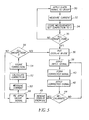
- the present invention operates as follows. Before a display device is used, a given input image signal is applied 30 to a group of light emitting elements, a measurement 32 of the current used by the display for the given input image signal is made.
- the given input image signal is typically a flat field of constant luminance across the group of light emitting elements in the display. This measurement may be taken once and assumed to apply to all similar devices or it may be taken for each individual display. In either case, the measurement is stored 34 in the controller circuit 16 and an initial correction signal set to 0. The process is repeated 35 for each group of light emitting elements. The display may then be put 36 into use. While in use, an input image signal is applied 38 to the controller 16 .
- the controller 16 corrects the input image signal for each group of light emitting elements to form 40 a corrected input image signal that is applied 42 to the display and the process repeats. Periodically a decision 44 is made to recalibrate the display. The display is removed from use 46 , the group image signals are re-applied 48 to each group of light emitting elements, and a measurement 50 of the display current taken again. The current measurements are then applied to the integrated model and corrected image signals calculated 52 and stored 54 . The process is repeated 56 for each group of light emitting elements. The display is then returned to use 36 so that as each new input image signal is applied 38 , the controller forms 40 a new corrected image signal and applies 42 the corrected image signal to the display.
- the controller circuit 16 will no longer be able to provide an image signal correction that is large enough and the display will have reached the end of its lifetime and can no longer meet its brightness or color specification. However, the display will continue to operate as its performance declines, thus providing a graceful degradation. Moreover, the time at which the display can no longer meet its specification can be signaled to a user of the display when a maximum correction is calculated, providing useful feedback on the performance of the display.
- the present invention can be constructed simply, requiring only (in addition to a conventional display controller) a current measurement circuit, a transformation means for the model to perform the image signal correction (for example a lookup table or amplifier), and a calculation circuit to determine the correction for the given image signal. No current accumulation or time information is necessary. Although the display must be periodically removed from use to perform the correction, the period may be quite large, for example days or tens of hours of use.
- the present invention can be used to correct for changes in color of a color display.
- the materials for each color emitter will age differently.
- a correction for the light emitting elements of the given color can be calculated.
- a separate model may be applied for each color, thus maintaining a consistent color for the display device.
- the given input image signals may be flat, uniform fields for each individual color corresponding to the OLED materials that emit the corresponding color.
- the present invention may be extended to include complex relationships between the corrected image signal, the measured current, and the aging of the materials.
- Multiple input image signals may be used corresponding to a variety of display outputs. For example, a different input image signal may correspond to each display output brightness level.
- a separate correction signal may be obtained for each display output brightness level by using different given input image signals.
- a separate correction signal is then employed for each display output brightness level required. As before, this can be done for each light emitting element grouping, for example different light emitting element color groups.
- the correction signals may correct for each display output brightness level of the display for each color as each material ages.
- the groups of light emitting elements and input image signals used to calculate the correction signals for the display device may also be spatially specific as well as color specific.
- the given input image signal may exercise only a subset, or even one light emitting element.
- the correction signals may apply to specific light emitting elements so that if a subset of light emitting elements age more rapidly, for example, if they are used more heavily (as an icon in a graphic user interface might), they may be corrected differently from other light emitting elements. Therefore, the present invention may correct for the aging of specific light emitting elements or groups of spatially distinct light emitting elements, and/or groups of colored light emitting elements. It is only necessary that a correction model be empirically derived for aging of each type of light emitting element or group of light emitting elements and that a periodic correction signal calculation be performed by driving the group of light emitting elements to be corrected.
- the correction calculation process may be performed periodically during use, at power-up or power-down.
- the correction calculation process may take only a few milliseconds so that the effect on any user is limited.
- the correction calculation process may be performed in response to a user signal supplied to the controller.
- OLED displays dissipate significant amounts of heat and become quite hot when used over long periods of time. Further experiments by applicant have determined that there is a strong relationship between temperature and current used by the display. Therefore, if the display has been in use for a period of time, the temperature of the display may need to be taken into account in calculating the correction signal. If it is assumed that the display has not been in use, or if the display is cooled, it may be assumed that the display is at a predetermined ambient temperature, for example room temperature. If the correction signal model was determined at that temperature, the temperature relationship may be ignored. If the display is calibrated at power-up and the correction signal model was determined at ambient temperature, this is a reasonable presumption in most cases. For example, mobile devices with a relatively frequent and short usage profile might not need temperature correction. Display applications for which the display is continuously on for longer periods, for example, monitors or televisions, might require temperature accommodation, or can be corrected on power-up to avoid display temperature issues.
- the display may be significantly hotter than the ambient temperature and it is preferred to accommodate the calibration by including the temperature effect. This can be done by measuring the temperature of the display, for example with a thermocouple placed on the substrate or cover of the device, or a temperature sensing element, such as a thermistor 17 (see Fig. 1), integrated into the electronics of the display. For displays that are constantly in use, the display is likely to be operated significantly above ambient temperature and the temperature can be taken into account for the display calibration.
- changes to the correction signals applied to the input image signals may be limited by the controller. Any change in correction can be limited in magnitude, for example to a 5% change.
- a calculated correction signal might also be restricted to be monotonically increasing, since the aging process does not reverse.
- Correction changes can also be averaged over time, for example an indicated correction change can be averaged with the previous value(s) to reduce variability.
- an actual correction can be made only after taking several readings, for example, every time the device is powered on, a corrections calculation is performed and a number of calculated correction signals (e.g. 10) are averaged to produce the actual correction signal that is applied to the device.
- the corrected image signal may take a variety of forms depending on the OLED display device. For example, if analog voltage levels are used to specify the image signal, the correction will modify the voltages of the image signal. This can be done using amplifiers as is known in the art. In a second example, if digital values are used, for example corresponding to a charge deposited at an active-matrix light emitting element location, a lookup table may be used to convert the digital value to another digital value as is well known in the art. In a typical OLED display device, either digital or analog video signals are used to drive the display. The actual OLED may be either voltage- or current-driven depending on the circuit used to pass current through the OLED. Again, these techniques are well known in the art.
- the correction signals used to modify the input image signal to form a corrected image signal may be used to implement a wide variety of display performance attributes over time.
- the model used to supply correction signals to an input image signal may hold the average luminance or white point of the display constant.
- the correction signals used to create the corrected image signal may allow the average luminance to degrade more slowly than it would otherwise due to aging.
- the invention is employed in a device that includes Organic Light Emitting Diodes (OLEDs) which are composed of small molecule or polymeric OLEDs as disclosed in but not limited to US 4,769,292, issued September 6, 1988 to Tang et al., and US 5,061,569, issued October 29, 1991 to VanSlyke et al. Many combinations and variations of organic light emitting displays can be used to fabricate such a device.
- OLEDs Organic Light Emitting Diodes
- the present invention can be employed in most OLED device configurations. These include very simple structures comprising a single anode and cathode to more complex devices, such as passive matrix displays comprised of orthogonal arrays of anodes and cathodes to form light emitting elements, and active-matrix displays where each light emitting element is controlled independently, for example, with thin film transistors (TFTs).
- TFTs thin film transistors
- a typical prior art structure is shown in Fig. 4 and is comprised of a substrate 101 , an anode 103 , a hole-injecting layer 105 , a hole-transporting layer 107 , a light-emitting layer 109 , an electron-transporting layer 111 , and a cathode 113 . These layers are described in detail below. Note that the substrate may alternatively be located adjacent to the cathode, or the substrate may actually constitute the anode or cathode.
- the organic layers between the anode and cathode are conveniently referred to as the organic EL element.
- the total combined thickness of the organic layers is preferably less than 500 nm.
- the anode and cathode of the OLED are connected to a voltage/current source 250 through electrical conductors 260 .
- the OLED is operated by applying a potential between the anode and cathode such that the anode is at a more positive potential than the cathode. Holes are injected into the organic EL element from the anode and electrons are injected into the organic EL element at the anode.
- Enhanced device stability can sometimes be achieved when the OLED is operated in an AC mode where, for some time period in the cycle, the potential bias is reversed and no current flows.
- An example of an AC-driven OLED is described in US 5,552,678.
- the OLED device of this invention is typically provided over a supporting substrate where either the cathode or anode can be in contact with the substrate.
- the electrode in contact with the substrate is conveniently referred to as the bottom electrode.
- the bottom electrode is the anode, but this invention is not limited to that configuration.
- the substrate can either be transmissive or opaque. In the case wherein the substrate is transmissive, a reflective or light absorbing layer is used to reflect the light through the cover or to absorb the light, thereby improving the contrast of the display.
- Substrates can include, but are not limited to, glass, plastic, semiconductor materials, silicon, ceramics, and circuit board materials. Of course it is necessary to provide a light-transparent top electrode.
- the anode When EL emission is viewed through anode 103, the anode should be transparent or substantially transparent to the emission of interest.
- Common transparent anode materials used in this invention are indium-tin oxide (ITO), indium-zinc oxide (IZO) and tin oxide, but other metal oxides can work including, but not limited to, aluminum- or indium-doped zinc oxide, magnesium-indium oxide, and nickel-tungsten oxide.
- metal nitrides such as gallium nitride
- metal selenides such as zinc selenide
- metal sulfides such as zinc sulfide
- anode For applications where EL emission is viewed only through the cathode electrode, the transmissive characteristics of anode are immaterial and any conductive material can be used, transparent, opaque or reflective.
- Example conductors for this application include, but are not limited to, gold, iridium, molybdenum, palladium, and platinum.
- Typical anode materials, transmissive or otherwise, have a work function of 4.1 eV or greater. Desired anode materials are commonly deposited by any suitable means such as evaporation, sputtering, chemical vapor deposition, or electrochemical means.
- Anodes can be patterned using well-known photolithographic processes.
- anodes may be polished prior to application of other layers to reduce surface roughness so as to minimize shorts or enhance reflectivity.
- hole-injecting layer 105 between anode 103 and hole-transporting layer 107 .
- the hole-injecting material can serve to improve the film formation property of subsequent organic layers and to facilitate injection of holes into the hole-transporting layer.
- Suitable materials for use in the hole-injecting layer include, but are not limited to, porphyrinic compounds as described in US 4,720,432, plasma-deposited fluorocarbon polymers as described in US 6,208,075, and some aromatic amines, for example, m-MTDATA (4,4',4"-tris[(3-methylphenyl)phenylamino]triphenylamine).
- Alternative hole-injecting materials reportedly useful in organic EL devices are described in EP 0 891 121 A1 and EP 1 029 909 A1.
- the hole-transporting layer 107 contains at least one hole-transporting compound such as an aromatic tertiary amine, where the latter is understood to be a compound containing at least one trivalent nitrogen atom that is bonded only to carbon atoms, at least one of which is a member of an aromatic ring.
- the aromatic tertiary amine can be an arylamine, such as a monoarylamine, diarylamine, triarylamine, or a polymeric arylamine. Exemplary monomeric triarylamines are illustrated by Klupfel et al. US 3,180,730.
- Other suitable triarylamines substituted with one or more vinyl radicals and/or comprising at least one active hydrogen containing group are disclosed by Brantley et al US 3,567,450 and 3,658,520.
- a more preferred class of aromatic tertiary amines are those which include at least two aromatic tertiary amine moieties as described in US 4,720,432 and 5,061,569.
- the hole-transporting layer can be formed of a single or a mixture of aromatic tertiary amine compounds.
- Illustrative of useful aromatic tertiary amines are the following:
- Another class of useful hole-transporting materials includes polycyclic aromatic compounds as described in EP 1 009 041. Tertiary aromatic amines with more than two amine groups may be used including oligomeric materials.
- polymeric hole-transporting materials can be used such as poly(N-vinylcarbazole) (PVK), polythiophenes, polypyrrole, polyaniline, and copolymers such as poly(3,4-ethylenedioxythiophene) / poly(4-styrenesulfonate) also called PEDOT/PSS.
- the light-emitting layer (LEL) 109 of the organic EL element includes a luminescent or fluorescent material where electroluminescence is produced as a result of electron-hole pair recombination in this region.
- the light-emitting layer can be comprised of a single material, but more commonly consists of a host material doped with a guest compound or compounds where light emission comes primarily from the dopant and can be of any color.
- the host materials in the light-emitting layer can be an electron-transporting material, as defined below, a hole-transporting material, as defined above, or another material or combination of materials that support hole-electron recombination.
- the dopant is usually chosen from highly fluorescent dyes, but phosphorescent compounds, e.g., transition metal complexes as described in WO 98/55561, WO 00/18851, WO 00/57676, and WO 00/70655 are also useful. Dopants are typically coated as 0.01 to 10 % by weight into the host material. Polymeric materials such as polyfluorenes and polyvinylarylenes (e.g., poly(p-phenylenevinylene), PPV) can also be used as the host material. In this case, small molecule dopants can be molecularly dispersed into the polymeric host, or the dopant could be added by copolymerizing a minor constituent into the host polymer.
- phosphorescent compounds e.g., transition metal complexes as described in WO 98/55561, WO 00/18851, WO 00/57676, and WO 00/70655 are also useful.
- Dopants are typically coated as 0.01
- bandgap potential is defined as the energy difference between the highest occupied molecular orbital and the lowest unoccupied molecular orbital of the molecule.
- band gap of the dopant is smaller than that of the host material.
- phosphorescent emitters it is also important that the host triplet energy level of the host be high enough to enable energy transfer from host to dopant.
- Host and emitting molecules known to be of use include, but are not limited to, those disclosed in US 4,768,292; 5,141,671; 5,150,006; 5,151,629; 5,405,709; 5,484,922; 5,593,788; 5,645,948; 5,683,823; 5,755,999; 5,928,802; 5,935,720; 5,935,721; and 6,020,078.
- Metal complexes of 8-hydroxyquinoline (oxine) and similar derivatives constitute one class of useful host compounds capable of supporting electroluminescence.
- useful chelated oxinoid compounds are the following:
- useful host materials include, but are not limited to: derivatives of anthracene, such as 9,10-di-(2-naphthyl)anthracene and derivatives thereof as described in US 5,935,721, distyrylarylene derivatives as described in US 5,121,029, and benzazole derivatives, for example, 2, 2', 2"-(1,3,5-phenylene)tris[1-phenyl-1H-benzimidazole].
- Carbazole derivatives are particularly useful hosts for phosphorescent emitters.
- Useful fluorescent dopants include, but are not limited to, derivatives of anthracene, tetracene, xanthene, perylene, rubrene, coumarin, rhodamine, and quinacridone, dicyanomethylenepyran compounds, thiopyran compounds, polymethine compounds, pyrilium and thiapyrilium compounds, fluorene derivatives, periflanthene derivatives, indenoperylene derivatives, bis(azinyl)amine boron compounds, bis(azinyl)methane compounds, and carbostyryl compounds.
- Preferred thin film-forming materials for use in forming the electron-transporting layer 111 of the organic EL elements of this invention are metal chelated oxinoid compounds, including chelates of oxine itself (also commonly referred to as 8-quinolinol or 8-hydroxyquinoline). Such compounds help to inject and transport electrons, exhibit high levels of performance, and are readily fabricated in the form of thin films. Exemplary oxinoid compounds were listed previously.
- electron-transporting materials include various butadiene derivatives as disclosed in US 4,356,429 and various heterocyclic optical brighteners as described in US 4,539,507. Benzazoles and triazines are also useful electron-transporting materials.
- the cathode 113 used in this invention can be comprised of nearly any conductive material. Desirable materials have good film-forming properties to ensure good contact with the underlying organic layer, promote electron injection at low voltage, and have good stability. Useful cathode materials often contain a low work function metal ( ⁇ 4.0 eV) or metal alloy.
- One preferred cathode material is comprised of a Mg:Ag alloy wherein the percentage of silver is in the range of 1 to 20 %, as described in US 4,885,221.
- cathode materials includes bilayers comprising a thin electron-injection layer (EIL) in contact with the organic layer (e.g., ETL) which is capped with a thicker layer of a conductive metal.
- EIL electron-injection layer
- the EIL preferably includes a low work function metal or metal salt, and if so, the thicker capping layer does not need to have a low work function.
- One such cathode is comprised of a thin layer of LiF followed by a thicker layer of Al as described in US 5,677,572.
- Other useful cathode material sets include, but are not limited to, those disclosed in US 5,059,861, 5,059,862, and 6,140,763.
- the cathode When light emission is viewed through the cathode, the cathode must be transparent or nearly transparent. For such applications, metals must be thin or one must use transparent conductive oxides, or a combination of these materials.
- Optically transparent cathodes have been described in more detail in US 4,885,211, US 5,247,190, JP 3,234,963, US 5,703,436, US 5,608,287, US 5,837,391, US 5,677,572, US 5,776,622, US 5,776,623, US 5,714,838, US 5,969,474, US 5,739,545, US 5,981,306, US 6,137,223, US 6,140,763, US 6,172,459, EP 1 076 368, US 6,278,236, and US 6,284,393.
- Cathode materials are typically deposited by evaporation, sputtering, or chemical vapor deposition. When needed, patterning can be achieved through many well known methods including, but not limited to, through-mask deposition, integral shadow masking, for example, as described in US 5,276,380 and EP 0 732 868, laser ablation, and selective chemical vapor deposition.
- layers 109 and 111 can optionally be collapsed into a single layer that serves the function of supporting both light emission and electron transportation.
- emitting dopants may be added to the hole-transporting layer, which may serve as a host. Multiple dopants may be added to one or more layers in order to create a white-emitting OLED, for example, by combining blue- and yellow-emitting materials, cyan- and red-emitting materials, or red-, green-, and blue-emitting materials.
- White-emitting devices are described, for example, in EP 1 187 235, US 20020025419, EP 1 182 244, US 5,683,823, US 5,503,910, US 5,405,709, and US 5,283,182.
- Additional layers such as electron or hole-blocking layers as taught in the art may be employed in devices of this invention.
- Hole-blocking layers are commonly used to improve efficiency of phosphorescent emitter devices, for example, as in US 20020015859.
- This invention may be used in so-called stacked device architecture, for example, as taught in US 5,703,436 and US 6,337,492.
- the organic materials mentioned above are suitably deposited through a vapor-phase method such as sublimation, but can be deposited from a fluid, for example, from a solvent with an optional binder to improve film formation. If the material is a polymer, solvent deposition is useful but other methods can be used, such as sputtering or thermal transfer from a donor sheet.
- the material to be deposited by sublimation can be vaporized from a sublimator "boat" often comprised of a tantalum material, e.g., as described in US 6,237,529, or can be first coated onto a donor sheet and then sublimed in closer proximity to the substrate.
- Layers with a mixture of materials can utilize separate sublimator boats or the materials can be pre-mixed and coated from a single boat or donor sheet. Patterned deposition can be achieved using shadow masks, integral shadow masks (US 5,294,870), spatially-defined thermal dye transfer from a donor sheet (US 5,688,551, 5,851,709 and 6,066,357) and inkjet method (US 6,066,357).
- OLED devices are sensitive to moisture or oxygen, or both, so they are commonly sealed in an inert atmosphere such as nitrogen or argon, along with a desiccant such as alumina, bauxite, calcium sulfate, clays, silica gel, zeolites, alkaline metal oxides, alkaline earth metal oxides, sulfates, or metal halides and perchlorates.
- a desiccant such as alumina, bauxite, calcium sulfate, clays, silica gel, zeolites, alkaline metal oxides, alkaline earth metal oxides, sulfates, or metal halides and perchlorates.
- Methods for encapsulation and desiccation include, but are not limited to, those described in US 6,226,890.
- barrier layers such as SiOx, Teflon, and alternating inorganic/polymeric layers are known in the art for encapsulation.
- OLED devices of this invention can employ various well-known optical effects in order to enhance its properties if desired. This includes optimizing layer thicknesses to yield maximum light transmission, providing dielectric mirror structures, replacing reflective electrodes with light-absorbing electrodes, providing anti glare or anti-reflection coatings over the display, providing a polarizing medium over the display, or providing colored, neutral density, or color conversion filters over the display. Filters, polarizers, and anti-glare or anti-reflection coatings may be specifically provided over the cover or an electrode protection layer beneath the cover.
Landscapes
- Engineering & Computer Science (AREA)
- Physics & Mathematics (AREA)
- Computer Hardware Design (AREA)
- General Physics & Mathematics (AREA)
- Theoretical Computer Science (AREA)
- Electroluminescent Light Sources (AREA)
- Control Of Indicators Other Than Cathode Ray Tubes (AREA)
- Control Of El Displays (AREA)
- Devices For Indicating Variable Information By Combining Individual Elements (AREA)
Applications Claiming Priority (2)
| Application Number | Priority Date | Filing Date | Title |
|---|---|---|---|
| US355922 | 1994-12-14 | ||
| US10/355,922 US7161566B2 (en) | 2003-01-31 | 2003-01-31 | OLED display with aging compensation |
Publications (2)
| Publication Number | Publication Date |
|---|---|
| EP1443484A2 true EP1443484A2 (fr) | 2004-08-04 |
| EP1443484A3 EP1443484A3 (fr) | 2010-02-17 |
Family
ID=32655591
Family Applications (1)
| Application Number | Title | Priority Date | Filing Date |
|---|---|---|---|
| EP04075154A Withdrawn EP1443484A3 (fr) | 2003-01-31 | 2004-01-19 | Ecran OLED à compensation de vieillissement |
Country Status (6)
| Country | Link |
|---|---|
| US (1) | US7161566B2 (fr) |
| EP (1) | EP1443484A3 (fr) |
| JP (2) | JP2004234011A (fr) |
| KR (1) | KR20040070106A (fr) |
| CN (1) | CN100483497C (fr) |
| TW (1) | TWI350123B (fr) |
Cited By (6)
| Publication number | Priority date | Publication date | Assignee | Title |
|---|---|---|---|---|
| WO2006037363A1 (fr) * | 2004-10-06 | 2006-04-13 | Fraunhofer-Gesellschaft zur Förderung der angewandten Forschung e.V. | Dispositif et procede pour commander une diode electroluminescente organique |
| WO2006062965A2 (fr) | 2004-12-09 | 2006-06-15 | Eastman Kodak Company | Affichage a diodes organiques electroluminescentes a compensation de vieillissement |
| WO2006125718A1 (fr) * | 2005-05-24 | 2006-11-30 | Thomson Licensing | Dispositif d'affichage d'images video a matrice active avec correction des non-uniformites de luminance |
| WO2007053783A1 (fr) * | 2005-11-07 | 2007-05-10 | Eastman Kodak Company | Afficheur à diodes électroluminescentes organiques avec compensation de vieillissement |
| WO2009026983A1 (fr) * | 2007-08-24 | 2009-03-05 | Ledon Lighting Gmbh | Procédé de détermination du flux lumineux d'une source de lumière |
| EP1784055A3 (fr) * | 2005-10-17 | 2009-08-05 | Semiconductor Energy Laboratory Co., Ltd. | Système d' éclairage |
Families Citing this family (127)
| Publication number | Priority date | Publication date | Assignee | Title |
|---|---|---|---|---|
| US8111222B2 (en) * | 2002-11-21 | 2012-02-07 | Koninklijke Philips Electronics N.V. | Method of improving the output uniformity of a display device |
| CA2419704A1 (fr) | 2003-02-24 | 2004-08-24 | Ignis Innovation Inc. | Methode de fabrication d'un pixel au moyen d'une diode electroluminescente organique |
| JP4808913B2 (ja) * | 2003-04-08 | 2011-11-02 | グローバル・オーエルイーディー・テクノロジー・リミテッド・ライアビリティ・カンパニー | 表示装置 |
| US7262753B2 (en) * | 2003-08-07 | 2007-08-28 | Barco N.V. | Method and system for measuring and controlling an OLED display element for improved lifetime and light output |
| CA2443206A1 (fr) | 2003-09-23 | 2005-03-23 | Ignis Innovation Inc. | Panneaux arriere d'ecran amoled - circuits de commande des pixels, architecture de reseau et compensation externe |
| US6870323B1 (en) * | 2003-10-02 | 2005-03-22 | Eastman Kodak Company | Color display with white light emitting elements |
| JP2005128089A (ja) * | 2003-10-21 | 2005-05-19 | Tohoku Pioneer Corp | 発光表示装置 |
| US6995519B2 (en) * | 2003-11-25 | 2006-02-07 | Eastman Kodak Company | OLED display with aging compensation |
| GB0328584D0 (en) * | 2003-12-10 | 2004-01-14 | Koninkl Philips Electronics Nv | Video data signal correction |
| EP1548573A1 (fr) * | 2003-12-23 | 2005-06-29 | Barco N.V. | Système de contrôle hiérarchique pour un affichage émissif à écran large en mosaique |
| US8025831B2 (en) * | 2004-05-24 | 2011-09-27 | Agency For Science, Technology And Research | Imprinting of supported and free-standing 3-D micro- or nano-structures |
| US7274346B2 (en) * | 2004-06-01 | 2007-09-25 | Eastman Kodak Company | Uniformity and brightness measurement in OLED displays |
| US7132805B2 (en) * | 2004-08-09 | 2006-11-07 | Dialight Corporation | Intelligent drive circuit for a light emitting diode (LED) light engine |
| US20060061292A1 (en) * | 2004-09-17 | 2006-03-23 | Samsung Electronics Co., Ltd. | Display device and driving method thereof |
| US7211452B2 (en) * | 2004-09-22 | 2007-05-01 | Eastman Kodak Company | Method and apparatus for uniformity and brightness correction in an OLED display |
| US7812800B2 (en) * | 2004-09-22 | 2010-10-12 | Tpo Displays Corp. | Design Approach and panel and electronic device utilizing the same |
| US20060077135A1 (en) * | 2004-10-08 | 2006-04-13 | Eastman Kodak Company | Method for compensating an OLED device for aging |
| US7400345B2 (en) * | 2004-10-22 | 2008-07-15 | Eastman Kodak Company | OLED display with aspect ratio compensation |
| US10013907B2 (en) | 2004-12-15 | 2018-07-03 | Ignis Innovation Inc. | Method and system for programming, calibrating and/or compensating, and driving an LED display |
| US10012678B2 (en) | 2004-12-15 | 2018-07-03 | Ignis Innovation Inc. | Method and system for programming, calibrating and/or compensating, and driving an LED display |
| TWI402790B (zh) | 2004-12-15 | 2013-07-21 | Ignis Innovation Inc | 用以程式化,校準及驅動一發光元件顯示器的方法及系統 |
| US9799246B2 (en) | 2011-05-20 | 2017-10-24 | Ignis Innovation Inc. | System and methods for extraction of threshold and mobility parameters in AMOLED displays |
| US8576217B2 (en) | 2011-05-20 | 2013-11-05 | Ignis Innovation Inc. | System and methods for extraction of threshold and mobility parameters in AMOLED displays |
| US7158106B2 (en) * | 2005-01-12 | 2007-01-02 | Eastman Kodak Company | Temperature measurement using an OLED device |
| CA2495726A1 (fr) | 2005-01-28 | 2006-07-28 | Ignis Innovation Inc. | Pixel programme par tension a reference locale pour affichages amoled |
| JP2006289721A (ja) * | 2005-04-08 | 2006-10-26 | Fuji Photo Film Co Ltd | 光走査装置における光量偏差補正方法 |
| KR100696107B1 (ko) * | 2005-04-11 | 2007-03-19 | 삼성전자주식회사 | 디스플레이장치 및 그 제어방법 |
| CN102663977B (zh) | 2005-06-08 | 2015-11-18 | 伊格尼斯创新有限公司 | 用于驱动发光器件显示器的方法和系统 |
| TWI309028B (en) * | 2005-06-13 | 2009-04-21 | Novatek Microelectronics Corp | Method for calibrating a flat panel display |
| US9318053B2 (en) * | 2005-07-04 | 2016-04-19 | Semiconductor Energy Laboratory Co., Ltd. | Semiconductor device and driving method thereof |
| US7391335B2 (en) * | 2005-08-18 | 2008-06-24 | Honeywell International, Inc. | Aerospace light-emitting diode (LED)-based lights life and operation monitor compensator |
| DE102005042704A1 (de) * | 2005-09-01 | 2007-03-08 | Ingenieurbüro Kienhöfer GmbH | Verfahren zum Betreiben einer Anzeigevorrichtung mit einer Mehrzahl von verschleißbehafteten Bildelementen und Anzeigevorrichtung |
| KR101333025B1 (ko) * | 2005-09-29 | 2013-11-26 | 코닌클리케 필립스 엔.브이. | 조명 디바이스의 노화 프로세스를 보상하는 방법 및 그조명 디바이스 |
| JP4694335B2 (ja) * | 2005-09-30 | 2011-06-08 | 富士フイルム株式会社 | 露光装置 |
| US8558765B2 (en) * | 2005-11-07 | 2013-10-15 | Global Oled Technology Llc | Method and apparatus for uniformity and brightness correction in an electroluminescent display |
| US20080055209A1 (en) * | 2006-08-30 | 2008-03-06 | Eastman Kodak Company | Method and apparatus for uniformity and brightness correction in an amoled display |
| JP2007156044A (ja) * | 2005-12-05 | 2007-06-21 | Sony Corp | 自発光表示装置、階調値/劣化率変換テーブル更新装置及びプログラム |
| US7505949B2 (en) * | 2006-01-31 | 2009-03-17 | Caterpillar Inc. | Process model error correction method and system |
| JP2007206464A (ja) * | 2006-02-02 | 2007-08-16 | Sony Corp | 自発光表示装置、見積もり劣化情報修正装置、入力表示データ補正装置及びプログラム |
| JP2007206463A (ja) * | 2006-02-02 | 2007-08-16 | Sony Corp | 自発光表示装置、入力表示データ補正装置及びプログラム |
| US20080048951A1 (en) * | 2006-04-13 | 2008-02-28 | Naugler Walter E Jr | Method and apparatus for managing and uniformly maintaining pixel circuitry in a flat panel display |
| CN101501748B (zh) | 2006-04-19 | 2012-12-05 | 伊格尼斯创新有限公司 | 有源矩阵显示器的稳定驱动设计 |
| US20070268414A1 (en) * | 2006-05-21 | 2007-11-22 | Ming-Tso Hsu | Method and system for distributing pvr functionalities |
| US20070290947A1 (en) * | 2006-06-16 | 2007-12-20 | Cok Ronald S | Method and apparatus for compensating aging of an electroluminescent display |
| US7696965B2 (en) * | 2006-06-16 | 2010-04-13 | Global Oled Technology Llc | Method and apparatus for compensating aging of OLED display |
| US20080042943A1 (en) * | 2006-06-16 | 2008-02-21 | Cok Ronald S | Method and apparatus for averaged luminance and uniformity correction in an am-el display |
| US8176319B2 (en) * | 2006-06-27 | 2012-05-08 | Emc Corporation | Identifying and enforcing strict file confidentiality in the presence of system and storage administrators in a NAS system |
| KR20080010796A (ko) * | 2006-07-28 | 2008-01-31 | 삼성전자주식회사 | 유기 발광 표시 장치 및 그의 구동 방법 |
| CA2556961A1 (fr) | 2006-08-15 | 2008-02-15 | Ignis Innovation Inc. | Technique de compensation de diodes electroluminescentes organiques basee sur leur capacite |
| GB2441354B (en) * | 2006-08-31 | 2009-07-29 | Cambridge Display Tech Ltd | Display drive systems |
| KR100787221B1 (ko) * | 2006-09-26 | 2007-12-21 | 삼성전자주식회사 | Led 기반 광시스템 및 그의 노화 보상방법 |
| TW200818973A (en) * | 2006-10-11 | 2008-04-16 | Au Optronics Corp | Temperature regulative display system and controlling method of amoled panel |
| US20080122759A1 (en) * | 2006-11-28 | 2008-05-29 | Levey Charles I | Active matrix display compensating method |
| KR101310376B1 (ko) * | 2006-12-20 | 2013-09-23 | 엘지디스플레이 주식회사 | 유기 발광다이오드 표시장치와 그 구동방법 |
| US7847764B2 (en) * | 2007-03-15 | 2010-12-07 | Global Oled Technology Llc | LED device compensation method |
| CN101295465B (zh) * | 2007-04-27 | 2010-12-22 | 深圳市同洲电子股份有限公司 | Led衰老校正方法及装置 |
| US8405585B2 (en) * | 2008-01-04 | 2013-03-26 | Chimei Innolux Corporation | OLED display, information device, and method for displaying an image in OLED display |
| FI122051B (fi) * | 2008-06-27 | 2011-07-29 | Valopaa Oy | Valaisin ja ohjausmenetelmä |
| US20100201275A1 (en) | 2009-02-06 | 2010-08-12 | Cok Ronald S | Light sensing in display device |
| US8350495B2 (en) | 2009-06-05 | 2013-01-08 | Light-Based Technologies Incorporated | Device driver providing compensation for aging |
| US9311859B2 (en) | 2009-11-30 | 2016-04-12 | Ignis Innovation Inc. | Resetting cycle for aging compensation in AMOLED displays |
| CA2669367A1 (fr) | 2009-06-16 | 2010-12-16 | Ignis Innovation Inc | Technique de compensation pour la variation chromatique des ecrans d'affichage . |
| US9384698B2 (en) | 2009-11-30 | 2016-07-05 | Ignis Innovation Inc. | System and methods for aging compensation in AMOLED displays |
| US10319307B2 (en) | 2009-06-16 | 2019-06-11 | Ignis Innovation Inc. | Display system with compensation techniques and/or shared level resources |
| US8633873B2 (en) | 2009-11-12 | 2014-01-21 | Ignis Innovation Inc. | Stable fast programming scheme for displays |
| CA2692097A1 (fr) | 2010-02-04 | 2011-08-04 | Ignis Innovation Inc. | Extraction de courbes de correlation pour des dispositifs luminescents |
| US10089921B2 (en) | 2010-02-04 | 2018-10-02 | Ignis Innovation Inc. | System and methods for extracting correlation curves for an organic light emitting device |
| US20140313111A1 (en) | 2010-02-04 | 2014-10-23 | Ignis Innovation Inc. | System and methods for extracting correlation curves for an organic light emitting device |
| US9881532B2 (en) | 2010-02-04 | 2018-01-30 | Ignis Innovation Inc. | System and method for extracting correlation curves for an organic light emitting device |
| US8711099B2 (en) | 2010-05-10 | 2014-04-29 | Blackberry Limited | Handheld electronic communication device having sliding display |
| JP2012073400A (ja) * | 2010-09-28 | 2012-04-12 | Sanyo Electric Co Ltd | 表示装置 |
| US8907991B2 (en) | 2010-12-02 | 2014-12-09 | Ignis Innovation Inc. | System and methods for thermal compensation in AMOLED displays |
| US8723890B2 (en) | 2010-12-23 | 2014-05-13 | Blackberry Limited | Handheld electronic device having sliding display and position configurable camera |
| US8514179B2 (en) | 2010-12-23 | 2013-08-20 | Research In Motion Limited | Handheld electronic communication device having an age compensating display |
| US9606607B2 (en) | 2011-05-17 | 2017-03-28 | Ignis Innovation Inc. | Systems and methods for display systems with dynamic power control |
| US9530349B2 (en) | 2011-05-20 | 2016-12-27 | Ignis Innovations Inc. | Charged-based compensation and parameter extraction in AMOLED displays |
| US9466240B2 (en) | 2011-05-26 | 2016-10-11 | Ignis Innovation Inc. | Adaptive feedback system for compensating for aging pixel areas with enhanced estimation speed |
| US9773439B2 (en) | 2011-05-27 | 2017-09-26 | Ignis Innovation Inc. | Systems and methods for aging compensation in AMOLED displays |
| US8901579B2 (en) | 2011-08-03 | 2014-12-02 | Ignis Innovation Inc. | Organic light emitting diode and method of manufacturing |
| US10089924B2 (en) | 2011-11-29 | 2018-10-02 | Ignis Innovation Inc. | Structural and low-frequency non-uniformity compensation |
| US9385169B2 (en) | 2011-11-29 | 2016-07-05 | Ignis Innovation Inc. | Multi-functional active matrix organic light-emitting diode display |
| US9324268B2 (en) | 2013-03-15 | 2016-04-26 | Ignis Innovation Inc. | Amoled displays with multiple readout circuits |
| KR101228885B1 (ko) * | 2011-12-21 | 2013-02-01 | 엘지디스플레이 주식회사 | 유기발광표시장치 및 그 제조방법 |
| US8937632B2 (en) | 2012-02-03 | 2015-01-20 | Ignis Innovation Inc. | Driving system for active-matrix displays |
| US8922544B2 (en) | 2012-05-23 | 2014-12-30 | Ignis Innovation Inc. | Display systems with compensation for line propagation delay |
| CN102768816B (zh) * | 2012-07-30 | 2015-09-23 | 西安诺瓦电子科技有限公司 | Led显示屏自动化校正方法 |
| US8922599B2 (en) | 2012-08-23 | 2014-12-30 | Blackberry Limited | Organic light emitting diode based display aging monitoring |
| KR101962897B1 (ko) | 2012-08-30 | 2019-03-29 | 삼성디스플레이 주식회사 | 화소 및 이를 이용한 유기전계발광 표시장치 |
| US9721505B2 (en) | 2013-03-08 | 2017-08-01 | Ignis Innovation Inc. | Pixel circuits for AMOLED displays |
| EP3043338A1 (fr) | 2013-03-14 | 2016-07-13 | Ignis Innovation Inc. | Re-interpolation avec détection de bord pour extraire un motif de vieillissement d'écrans amoled |
| WO2014140992A1 (fr) | 2013-03-15 | 2014-09-18 | Ignis Innovation Inc. | Réglage dynamique des résolutions tactiles d'un écran amoled |
| US9741282B2 (en) | 2013-12-06 | 2017-08-22 | Ignis Innovation Inc. | OLED display system and method |
| US9761170B2 (en) | 2013-12-06 | 2017-09-12 | Ignis Innovation Inc. | Correction for localized phenomena in an image array |
| US9059337B1 (en) * | 2013-12-24 | 2015-06-16 | Christie Digital Systems Usa, Inc. | Method, system and apparatus for dynamically monitoring and calibrating display tiles |
| US9502653B2 (en) | 2013-12-25 | 2016-11-22 | Ignis Innovation Inc. | Electrode contacts |
| US10997901B2 (en) | 2014-02-28 | 2021-05-04 | Ignis Innovation Inc. | Display system |
| US10176752B2 (en) | 2014-03-24 | 2019-01-08 | Ignis Innovation Inc. | Integrated gate driver |
| DE102015206281A1 (de) | 2014-04-08 | 2015-10-08 | Ignis Innovation Inc. | Anzeigesystem mit gemeinsam genutzten Niveauressourcen für tragbare Vorrichtungen |
| CN103927989B (zh) * | 2014-04-21 | 2016-09-21 | 中国电子科技集团公司第五十五研究所 | 具有宽温亮度补偿功能的无源有机发光二极管显示装置及亮度补偿方法 |
| CN109346005B (zh) * | 2014-06-26 | 2021-10-01 | 萤光勒克斯株式会社 | 有机el面板控制装置、光源装置、有机el面板控制方法、程序以及记录介质 |
| CN104361859B (zh) * | 2014-11-18 | 2017-01-11 | 深圳市华星光电技术有限公司 | 显示装置及其亮度调节方法 |
| CA2872563A1 (fr) | 2014-11-28 | 2016-05-28 | Ignis Innovation Inc. | Architecture de reseau a densite de pixels elevee |
| TWI540566B (zh) * | 2014-12-09 | 2016-07-01 | 緯創資通股份有限公司 | 顯示器及其亮度、色彩補償方法與系統 |
| CA2879462A1 (fr) | 2015-01-23 | 2016-07-23 | Ignis Innovation Inc. | Compensation de la variation de couleur dans les dispositifs emetteurs |
| CA2889870A1 (fr) | 2015-05-04 | 2016-11-04 | Ignis Innovation Inc. | Systeme de retroaction optique |
| CA2892714A1 (fr) | 2015-05-27 | 2016-11-27 | Ignis Innovation Inc | Reduction de largeur de bande de memoire dans un systeme de compensation |
| US10373554B2 (en) | 2015-07-24 | 2019-08-06 | Ignis Innovation Inc. | Pixels and reference circuits and timing techniques |
| CA2898282A1 (fr) | 2015-07-24 | 2017-01-24 | Ignis Innovation Inc. | Etalonnage hybride de sources de courant destine a des afficheurs a tension polarisee par courant programmes |
| US10657895B2 (en) | 2015-07-24 | 2020-05-19 | Ignis Innovation Inc. | Pixels and reference circuits and timing techniques |
| KR102435923B1 (ko) * | 2015-08-05 | 2022-08-25 | 삼성디스플레이 주식회사 | 유기 발광 표시 장치 및 이의 구동 방법 |
| CA2900170A1 (fr) | 2015-08-07 | 2017-02-07 | Gholamreza Chaji | Etalonnage de pixel fonde sur des valeurs de reference ameliorees |
| CA2909813A1 (fr) | 2015-10-26 | 2017-04-26 | Ignis Innovation Inc | Orientation de motif ppi dense |
| CN105825797B (zh) * | 2016-03-31 | 2020-01-14 | Oppo广东移动通信有限公司 | 一种显示屏的检测方法、检测装置以及终端 |
| CN105895056B (zh) | 2016-06-17 | 2017-04-19 | 京东方科技集团股份有限公司 | 亮度补偿模型的建立方法、屏幕亮度的补偿方法及装置 |
| CN106093529B (zh) | 2016-07-19 | 2019-03-12 | 京东方科技集团股份有限公司 | 电流测量校准方法、电流测量方法及装置、显示装置 |
| US10586491B2 (en) | 2016-12-06 | 2020-03-10 | Ignis Innovation Inc. | Pixel circuits for mitigation of hysteresis |
| US10714018B2 (en) | 2017-05-17 | 2020-07-14 | Ignis Innovation Inc. | System and method for loading image correction data for displays |
| KR102326166B1 (ko) * | 2017-06-30 | 2021-11-16 | 엘지디스플레이 주식회사 | 전계 발광 표시장치와 그 구동방법 |
| CN109307587B (zh) * | 2017-07-26 | 2020-01-31 | 京东方科技集团股份有限公司 | 显示面板检测方法、装置及系统 |
| US11025899B2 (en) | 2017-08-11 | 2021-06-01 | Ignis Innovation Inc. | Optical correction systems and methods for correcting non-uniformity of emissive display devices |
| KR102644412B1 (ko) * | 2017-11-16 | 2024-03-06 | 시냅틱스 인코포레이티드 | 디스플레이 패널을 위한 보상 기술 |
| US10971078B2 (en) | 2018-02-12 | 2021-04-06 | Ignis Innovation Inc. | Pixel measurement through data line |
| KR20190100577A (ko) * | 2018-02-21 | 2019-08-29 | 삼성전자주식회사 | 픽셀의 열화량을 산출하는 전자 장치 |
| KR102033460B1 (ko) * | 2018-04-30 | 2019-10-17 | 배재대학교 산학협력단 | Oled 에이징 시스템 및 방법 |
| JP2021071680A (ja) * | 2019-11-01 | 2021-05-06 | セイコーエプソン株式会社 | 表示装置、頭部装着型表示装置および表示方法 |
| TWI809997B (zh) * | 2022-07-28 | 2023-07-21 | 大陸商北京集創北方科技股份有限公司 | Led顯示驅動的色溫補償方法、led顯示驅動晶片及led顯示裝置 |
| TWI845226B (zh) * | 2023-03-24 | 2024-06-11 | 友達光電股份有限公司 | 亮度補償裝置及亮度補償方法 |
Citations (5)
| Publication number | Priority date | Publication date | Assignee | Title |
|---|---|---|---|---|
| EP0923067A1 (fr) | 1997-03-12 | 1999-06-16 | Seiko Epson Corporation | Circuit pixel, afficheur, et equipement electronique a dispositif photoemetteur commande par courant |
| EP1079361A1 (fr) * | 1999-08-20 | 2001-02-28 | Harness System Technologies Research, Ltd. | Circuit d'attaque pour éléments électroluminescents |
| WO2001027910A1 (fr) * | 1999-10-12 | 2001-04-19 | Koninklijke Philips Electronics N.V. | Afficheur a diode electroluminescente |
| EP1227466A2 (fr) | 2001-01-29 | 2002-07-31 | Semiconductor Energy Laboratory Co., Ltd. | Dispositif électroluminescent |
| JP2002278514A (ja) | 2001-03-19 | 2002-09-27 | Sharp Corp | 電気光学装置 |
Family Cites Families (18)
| Publication number | Priority date | Publication date | Assignee | Title |
|---|---|---|---|---|
| JP3106953B2 (ja) * | 1996-05-16 | 2000-11-06 | 富士電機株式会社 | 表示素子駆動方法 |
| JP3767877B2 (ja) * | 1997-09-29 | 2006-04-19 | 三菱化学株式会社 | アクティブマトリックス発光ダイオード画素構造およびその方法 |
| JP2000056732A (ja) * | 1998-08-12 | 2000-02-25 | Tdk Corp | 有機el表示装置 |
| US6504565B1 (en) | 1998-09-21 | 2003-01-07 | Canon Kabushiki Kaisha | Light-emitting device, exposure device, and image forming apparatus |
| CN1377495A (zh) * | 1999-10-04 | 2002-10-30 | 松下电器产业株式会社 | 显示面板的驱动方法、显示面板的亮度校正装置及其驱动装置 |
| US6414661B1 (en) | 2000-02-22 | 2002-07-02 | Sarnoff Corporation | Method and apparatus for calibrating display devices and automatically compensating for loss in their efficiency over time |
| EP1158483A3 (fr) * | 2000-05-24 | 2003-02-05 | Eastman Kodak Company | Affichage à l'état solide avec pixel de référence |
| US20020030647A1 (en) * | 2000-06-06 | 2002-03-14 | Michael Hack | Uniform active matrix oled displays |
| JP2002215094A (ja) * | 2001-01-16 | 2002-07-31 | Sony Corp | 画像表示装置とその駆動方法 |
| SG111928A1 (en) * | 2001-01-29 | 2005-06-29 | Semiconductor Energy Lab | Light emitting device |
| TWI248319B (en) * | 2001-02-08 | 2006-01-21 | Semiconductor Energy Lab | Light emitting device and electronic equipment using the same |
| US6963321B2 (en) | 2001-05-09 | 2005-11-08 | Clare Micronix Integrated Systems, Inc. | Method of providing pulse amplitude modulation for OLED display drivers |
| US6944424B2 (en) * | 2001-07-23 | 2005-09-13 | Intermec Ip Corp. | RFID tag having combined battery and passive power source |
| US6456016B1 (en) | 2001-07-30 | 2002-09-24 | Intel Corporation | Compensating organic light emitting device displays |
| SG120888A1 (en) * | 2001-09-28 | 2006-04-26 | Semiconductor Energy Lab | A light emitting device and electronic apparatus using the same |
| JP2003122305A (ja) * | 2001-10-10 | 2003-04-25 | Sony Corp | 有機el表示装置およびその制御方法 |
| JP4293747B2 (ja) * | 2001-12-26 | 2009-07-08 | ソニー株式会社 | 有機el表示装置およびその制御方法 |
| JP4593868B2 (ja) * | 2002-05-14 | 2010-12-08 | ソニー株式会社 | 表示装置およびその駆動方法 |
-
2003
- 2003-01-31 US US10/355,922 patent/US7161566B2/en not_active Expired - Lifetime
- 2003-12-09 TW TW092134692A patent/TWI350123B/zh not_active IP Right Cessation
-
2004
- 2004-01-19 EP EP04075154A patent/EP1443484A3/fr not_active Withdrawn
- 2004-01-30 JP JP2004023121A patent/JP2004234011A/ja not_active Withdrawn
- 2004-01-31 KR KR1020040006474A patent/KR20040070106A/ko not_active Ceased
- 2004-01-31 CN CNB2004100038467A patent/CN100483497C/zh not_active Expired - Lifetime
-
2011
- 2011-09-05 JP JP2011192282A patent/JP2012027481A/ja active Pending
Patent Citations (5)
| Publication number | Priority date | Publication date | Assignee | Title |
|---|---|---|---|---|
| EP0923067A1 (fr) | 1997-03-12 | 1999-06-16 | Seiko Epson Corporation | Circuit pixel, afficheur, et equipement electronique a dispositif photoemetteur commande par courant |
| EP1079361A1 (fr) * | 1999-08-20 | 2001-02-28 | Harness System Technologies Research, Ltd. | Circuit d'attaque pour éléments électroluminescents |
| WO2001027910A1 (fr) * | 1999-10-12 | 2001-04-19 | Koninklijke Philips Electronics N.V. | Afficheur a diode electroluminescente |
| EP1227466A2 (fr) | 2001-01-29 | 2002-07-31 | Semiconductor Energy Laboratory Co., Ltd. | Dispositif électroluminescent |
| JP2002278514A (ja) | 2001-03-19 | 2002-09-27 | Sharp Corp | 電気光学装置 |
Cited By (11)
| Publication number | Priority date | Publication date | Assignee | Title |
|---|---|---|---|---|
| WO2006037363A1 (fr) * | 2004-10-06 | 2006-04-13 | Fraunhofer-Gesellschaft zur Förderung der angewandten Forschung e.V. | Dispositif et procede pour commander une diode electroluminescente organique |
| WO2006062965A2 (fr) | 2004-12-09 | 2006-06-15 | Eastman Kodak Company | Affichage a diodes organiques electroluminescentes a compensation de vieillissement |
| WO2006062965A3 (fr) * | 2004-12-09 | 2006-08-03 | Eastman Kodak Co | Affichage a diodes organiques electroluminescentes a compensation de vieillissement |
| WO2006125718A1 (fr) * | 2005-05-24 | 2006-11-30 | Thomson Licensing | Dispositif d'affichage d'images video a matrice active avec correction des non-uniformites de luminance |
| EP1784055A3 (fr) * | 2005-10-17 | 2009-08-05 | Semiconductor Energy Laboratory Co., Ltd. | Système d' éclairage |
| US8154192B2 (en) | 2005-10-17 | 2012-04-10 | Semiconductor Energy Laboratory Co., Ltd. | Lighting system |
| US8441184B2 (en) | 2005-10-17 | 2013-05-14 | Semiconductor Energy Laboratory Co., Ltd. | Lighting system |
| WO2007053783A1 (fr) * | 2005-11-07 | 2007-05-10 | Eastman Kodak Company | Afficheur à diodes électroluminescentes organiques avec compensation de vieillissement |
| EP1982320A1 (fr) * | 2005-11-07 | 2008-10-22 | Eastman Kodak Company | Afficheur a diodes electroluminescentes organiques avec compensation de vieillissement |
| KR101310935B1 (ko) * | 2005-11-07 | 2013-09-23 | 글로벌 오엘이디 테크놀러지 엘엘씨 | 영상 신호 보정 방법 및 이를 사용하는 oled디스플레이 |
| WO2009026983A1 (fr) * | 2007-08-24 | 2009-03-05 | Ledon Lighting Gmbh | Procédé de détermination du flux lumineux d'une source de lumière |
Also Published As
| Publication number | Publication date |
|---|---|
| CN1519796A (zh) | 2004-08-11 |
| JP2012027481A (ja) | 2012-02-09 |
| JP2004234011A (ja) | 2004-08-19 |
| US7161566B2 (en) | 2007-01-09 |
| KR20040070106A (ko) | 2004-08-06 |
| TWI350123B (en) | 2011-10-01 |
| CN100483497C (zh) | 2009-04-29 |
| US20040150590A1 (en) | 2004-08-05 |
| EP1443484A3 (fr) | 2010-02-17 |
| TW200414807A (en) | 2004-08-01 |
Similar Documents
| Publication | Publication Date | Title |
|---|---|---|
| US7161566B2 (en) | OLED display with aging compensation | |
| US6995519B2 (en) | OLED display with aging compensation | |
| US7355574B1 (en) | OLED display with aging and efficiency compensation | |
| US8207914B2 (en) | OLED display with aging compensation | |
| EP2160728B1 (fr) | Methode de compensation de vieillissement d'un ecran à diodes électroluminescentes organiques | |
| US6919681B2 (en) | Color OLED display with improved power efficiency | |
| US6747618B2 (en) | Color organic light emitting diode display with improved lifetime | |
| US7973473B2 (en) | Flat panel OLED device having deformable substrate | |
| US20060261732A1 (en) | Color organic light-emitting diode display with improved lifetime |
Legal Events
| Date | Code | Title | Description |
|---|---|---|---|
| PUAI | Public reference made under article 153(3) epc to a published international application that has entered the european phase |
Free format text: ORIGINAL CODE: 0009012 |
|
| AK | Designated contracting states |
Kind code of ref document: A2 Designated state(s): AT BE BG CH CY CZ DE DK EE ES FI FR GB GR HU IE IT LI LU MC NL PT RO SE SI SK TR |
|
| AX | Request for extension of the european patent |
Extension state: AL LT LV MK |
|
| PUAL | Search report despatched |
Free format text: ORIGINAL CODE: 0009013 |
|
| AK | Designated contracting states |
Kind code of ref document: A3 Designated state(s): AT BE BG CH CY CZ DE DK EE ES FI FR GB GR HU IE IT LI LU MC NL PT RO SE SI SK TR |
|
| AX | Request for extension of the european patent |
Extension state: AL LT LV MK |
|
| RAP1 | Party data changed (applicant data changed or rights of an application transferred) |
Owner name: GLOBAL OLED TECHNOLOGY LLC |
|
| 17P | Request for examination filed |
Effective date: 20100427 |
|
| AKX | Designation fees paid |
Designated state(s): DE FR GB |
|
| 17Q | First examination report despatched |
Effective date: 20101125 |
|
| RAP1 | Party data changed (applicant data changed or rights of an application transferred) |
Owner name: GLOBAL OLED TECHNOLOGY LLC |
|
| STAA | Information on the status of an ep patent application or granted ep patent |
Free format text: STATUS: THE APPLICATION IS DEEMED TO BE WITHDRAWN |
|
| 18D | Application deemed to be withdrawn |
Effective date: 20150310 |