EP1443672A2 - Procédé, appareil et programme de détermination de chemins - Google Patents
Procédé, appareil et programme de détermination de chemins Download PDFInfo
- Publication number
- EP1443672A2 EP1443672A2 EP04001943A EP04001943A EP1443672A2 EP 1443672 A2 EP1443672 A2 EP 1443672A2 EP 04001943 A EP04001943 A EP 04001943A EP 04001943 A EP04001943 A EP 04001943A EP 1443672 A2 EP1443672 A2 EP 1443672A2
- Authority
- EP
- European Patent Office
- Prior art keywords
- power level
- samples
- weighing
- power
- change
- Prior art date
- Legal status (The legal status is an assumption and is not a legal conclusion. Google has not performed a legal analysis and makes no representation as to the accuracy of the status listed.)
- Granted
Links
Images
Classifications
-
- H—ELECTRICITY
- H04—ELECTRIC COMMUNICATION TECHNIQUE
- H04B—TRANSMISSION
- H04B1/00—Details of transmission systems, not covered by a single one of groups H04B3/00 - H04B13/00; Details of transmission systems not characterised by the medium used for transmission
- H04B1/69—Spread spectrum techniques
- H04B1/707—Spread spectrum techniques using direct sequence modulation
- H04B1/7097—Interference-related aspects
- H04B1/711—Interference-related aspects the interference being multi-path interference
- H04B1/7113—Determination of path profile
-
- H—ELECTRICITY
- H04—ELECTRIC COMMUNICATION TECHNIQUE
- H04B—TRANSMISSION
- H04B1/00—Details of transmission systems, not covered by a single one of groups H04B3/00 - H04B13/00; Details of transmission systems not characterised by the medium used for transmission
- H04B1/69—Spread spectrum techniques
- H04B1/707—Spread spectrum techniques using direct sequence modulation
- H04B1/7097—Interference-related aspects
- H04B1/711—Interference-related aspects the interference being multi-path interference
- H04B1/7115—Constructive combining of multi-path signals, i.e. RAKE receivers
- H04B1/7117—Selection, re-selection, allocation or re-allocation of paths to fingers, e.g. timing offset control of allocated fingers
Definitions
- the present invention relates to a path searching circuit, a path searching method, and a path searching program and more particularly to the path searching circuit, the path searching method, and the path searching program being preferably employed in a CDMA (Code Division Multiple Access) communication system.
- CDMA Code Division Multiple Access
- a path diversity effect is achieved, conventionally, by path searching and rake combining.
- Quality of a radio wave received in a mobile telecommunication environment is degraded by a change in power levels and/or noises caused by multi-path fading.
- frequency of an error in detecting signal receiving path timing at time of searching a path becomes high, which causes degradation of a signal receiving characteristic. Therefore, advent of path searching processing is expected in which a stable path can be searched out of arriving paths and can be assigned to a finger.
- a conventional path searching device is disclosed in, for example, Japanese Patent Application Laid-open No. 2001 - 36430, in which a judgment is made on whether or not an interpolation process to make a chip interval smaller is performed before and after each individual processing unit for every two or more processing units depending on the number of communication channels to be processed and the interpolation process is then performed, based on a result from the judgement, before and after each individual processing unit in a path searching processing steps.
- a path searching circuit employed in a CDMA communication system including:
- a preferable mode is one wherein the weighing controlling unit saves a sample whose power level exceeds a power threshold value as a candidate for weighing control.
- a preferable mode is one wherein the weighing controlling unit, when a number of samples of a candidate for the weighing control is 1 (one), assigns negative weight to a power level of the sample.
- a preferable mode is one wherein the weighing controlling unit, when a number of samples of the candidate for the weighing control is two or more and when a difference in power levels among specified samples is a change threshold value or more, assigns negative weight to power levels of the two or more samples.
- a preferable mode is one wherein the weight assigned to the power level of the specified sample by the weighing controlling unit is determined based on any one of a fixed value, a maximum power level, and an amount of a change in a power level.
- a preferable mode is one wherein, in comparison between the change threshold value and a difference in power levels among specified samples, when a number of samples of the candidate for the weighing control is 2 (two), a difference in power levels between the two samples is compared with the change threshold value and when a number of samples of the candidate for the weighing control is 3 (three) or more, a difference between a maximum power level and a minimum power level is compared with the change threshold value or a difference in power levels among samples of delay profiles existing before and after one another in terms of time is compared with the change threshold value.
- a path searching method employed in a CDMA communication system including:
- a preferable mode is one wherein, in the weighing controlling step, a sample whose power level exceeds a power threshold is saved as a candidate for weighing control.
- a preferable mode is one wherein, in the weighing controlling step, when a number of samples of a candidate for the weighing control is 1 (one) , negative weight is assigned to a power level of the sample.
- a preferable mode is one wherein, in the weighing controlling step, when a number of samples of the candidate for the weighing control is two or more and when a difference in power levels among specified samples is a change threshold value or more, negative weight is assigned to power levels of the two or more samples.
- a preferable mode is one wherein the weight assigned to the power level of the specified sample in the weighing controlling step is determined based on any one of a fixed value, a maximum power level, and an amount of a change in a power level.
- a preferable mode is one wherein, in comparison between the change threshold value and a difference in power levels among specified samples, when a number of samples of the candidate for the weighing control is 2 (two), a difference in power levels between the two samples is compared with the change threshold value and when a number of samples of the candidate for the weighing control is 3 (three) or more, a difference between a maximum power level and a minimum power level is compared with the change threshold value or a difference in power levels among samples of delay profiles existing before and after one another in terms of time is compared with the change threshold value.
- a path searching program for having a computer execute a path searching method employed in a CDMA communication system including:
- a preferable mode is one wherein, in the weighing controlling step, a sample whose power level exceeds a power threshold is saved as a candidate for weighing control.
- a preferable mode is one wherein, in the weighing controlling step, when a number of samples of a candidate for the weighing control is 1 (one) , negative weight is assigned to a power level of the sample.
- a preferable mode is one wherein, in the weighing controlling step, when a number of samples of the candidate for the weighing control is two or more and when a difference in power levels among specified samples is a change threshold value or more, negative weight is assigned to power levels of the two or more samples.
- a preferable mode is one wherein the weight assigned to the power level of the specified sample in the weighing controlling step is determined based on any one of a fixed value, a maximum power level, and an amount of a change in a power level.
- a preferable mode is one wherein, in comparison between the change threshold value and a difference in power levels among specified samples, when a number of samples of the candidate for the weighing control is 2 (two), a difference in power levels between the two samples is compared with the change threshold value and when a number of samples of the candidate for the weighing control is 3 (three) or more, a difference between a maximum power level and a minimum power level is compared with the change threshold value or a power level difference among samples of delay profiles existing before and after one another in terms of time is compared with the change threshold value.
- a first effect is that an error in detecting signal receiving path timing caused by noises can be reduced, thus enabling an excellent signal receiving characteristic to be obtained.
- a reason is that, by monitoring a power level of a delay profile and by exercising weighing control in delay profile power adding processes, it is possible to create an average delay profile in which an influence by an instantaneous high power level caused by noises is reduced. In other words, in the calculation of delay profiles, according to changes in levels of correlation values, by adaptively controlling delay profile averaging processing, a stable path is searched, thus achieving the excellent signal receiving characteristic.
- a second effect is that a path change in mobile telecommunications can be quickly tracked and responded, enabling an excellent signal receiving characteristic to be achieved.
- a reason is that, by creating a delay profile with influences caused by noises being reduced, an average time of the delay profile is shortened and the path searching processing is speeded up.
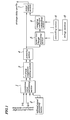
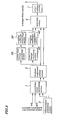
- FIG. 1 is a diagram showing configurations of one example of a delay profile calculating circuit employed in a path searching circuit according to an embodiment of the present invention.
- the delay profile calculating circuit includes a correlation value calculating section 1, a diffused signal generating section 2, an in-phase component adding section 3, a powering section 4, a power level change monitoring section 5, a weighing coefficient controlling section 6, a power adding section 7, a controlling section 8, and a storage medium 9.
- the in-phase component adding section 3 performs an adding calculation of in-phase components between the I component correlation value and the Q component correlation value.
- the powering section 4 powers the correlation value obtained by the adding calculation of in-phase components and calculates the delay profile.
- the power adding section 7 performs an averaging process on the obtained delay profile to smooth changes in power levels caused by noises and/or fading and calculates an average delay profile.
- a portable terminal estimates signal receiving path timing by using the average delay profile, that is, searches a path and performs a demodulating process.
- the delay profile output from the powering section 4 is input to the power level change monitoring section 5 and a change in a power level of each sample of two or more delay profiles to be used for same power adding processing is monitored by the power level change monitoring section 5.
- the weighing coefficient controlling section 6 by using the above result, when power is added by the power adding section 7, a weighing coefficient is controlled on a sample of the delay profile being estimated to be at a high power level caused by noises so that the power level becomes low.
- the power level change monitoring section 5 monitors a change in power levels of each of the delay profiles and inputs a result from the monitoring process to the weighing coefficient controlling section 6.
- the weighing coefficient controlling section 6 in the case of sampling timing with which a result showing that the change in power levels of the delay profile is small occurs in the power averaging process in the power adding section 7, adding processing is performed with the sampling timing without weight being assigned to the power level, and, in the case of sampling timing with which a result showing that the change in power levels of the delay profile is large occurs, weight is assigned to the power level in the power adding processing and the weighing is controlled so that it is observed that the power level obtained after the averaging process is lower than that obtained by simply adding processing.
- the controlling section 8 controls the power level change monitoring section 5 and the weighing coefficient controlling section 6.
- the storage medium 9 stores a path searching program to have a computer (controlling section 8) execute the patch searching method of this embodiment.
- the controlling section 8 exerts control on the power level change monitoring section 5 and the weighing coefficient controlling section 6 according to the path searching program stored in the storage medium 9. Contents of the path searching program are described later.
- FIG. 1 A first examples of the embodiment is explained by referring to Fig. 1. Configurations of a delay profile calculating circuit employed in the first example are the same as shown in Fig. 1.
- Each of an I component signal and a Q component signal having undergone quadrature detection and demodulation is input to the correlation value calculating section 1.
- the correlation value calculating section 1 calculates correlation values between a diffused signal generated by the diffused signal generating section 2 and the input I component signal and the Q component signal. Since there is a correlation between the diffused signal generated by the diffused signal generating section 2 and the received I and Q component signals in the CDMA communications, the calculation shows that there is a highly correlated value between the diffused signal and the I and Q component signals that are detected with signal receiving path timing.
- the resulting correlated values are input to the in-phase component adding section 3, where, in order to improve an S/N ratio of the delay profile, adding calculation of in-phase components in the correlation values of the I component and the Q component is performed.
- the correlation values obtained after the adding calculation of the in-phase components are input to the powering section 4, where powering calculation is performed on the input values and then are output as a delay profile.
- a power level obtained with each of sampling timing for two or more delay profiles to be used for processing of adding same power is monitored and a sample whose power level exceeds a power threshold "P _ th" is saved as a candidate for weighing control and then a result from the monitoring is input to the weighing coefficient controlling section 6.
- the power level change detected with the same sampling timing is the change threshold value "Lev _ th" or more, it is judged that the high power level is detected not with the signal receiving path timing but with sampling timing with which the power level is instantaneously high and changes greatly due to an influence by noises or a like and, when power adding processing is performed by the power adding section 7 using two or more delay profiles, a weighing coefficient W ( ⁇ 0) is determined so that an influence by the power level detected with sampling timing with which the power level is affected by noises or a like is reduced.
- the power adding section 7 performs power adding processing for two or more delay profiles to smooth power changes caused by noises and/or fading, since the power adding processing is performed by using a weighing coefficient determined by the weighing coefficient controlling section 6, calculation of the average delay profile is possible in which the influence by the instantaneous high power level caused by noises is reduced.
- a first method is to fix a value, in advance, as the weighing coefficient W.
- a second method is to control the weighing coefficient W in accordance with a maximum power level of the delay profile. For example, if the maximum power level of the delay profile is X0 dB, the weighing coefficient W is set to be W0. If the maximum power level of the delay profile is X1 dB, the weighing coefficient W is set to be W1. Moreover, it is possible that the maximum power level is the maximum power level of the delay profile in the past.
- a third method is to control a weighing coefficient W in accordance with an amount of a change in power levels. For example, if the amount of the change in power levels is Y0dB, the weighing coefficient is W0 and if the amount of the change in power levels is Y1dB, the weighing coefficient is W1.
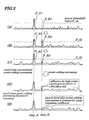
- FIG. 1 is a diagram illustrating time-consecutive delay profiles output from the powering section 4.
- the power adding section 7 shown in Fig. 1 let the number of power adding profiles be "3" as an example.
- a sampling point see a point Smp-A in waveforms (A) to (C) of Fig. 2 detected with signal receiving path timing, since held is a correlation between a diffused signal generated by the diffused signal generating section 2 and an output having underdone quadrature detection, high power levels are consecutively detected with same timing.
- the power level of the input delay profile and its level change detected at a sampling point are monitored and a result from the monitoring is input to the weighing coefficient controlling section 6.
- sampling timing with which a power level is greatly changed is judged to be incorrect sampling timing and a weighing coefficient is determined so that an influence on an average delay profile to be obtained after power adding processing is reduced.
- a weighing coefficient (W ⁇ 1) is determined by monitoring the power level change, and, in power adding processing, power adding calculation is done using a following expression with the sampling timing "Smp _ B" shown in waveform (E) of Fig. 2 with which the power level change shown as "P _ B2" in waveform (B) of Fig. 2 being judged to be influenced by noises is detected: P_B1 + W x P_B2 + P_B3
- an error in detecting signal receiving path timing in a path searching process can be reduced, thus improving a signal receiving characteristic.
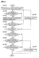
- FIG. 3 is a flowchart showing procedures for the weighing coefficient control processing.
- the number of power adding profiles in the power adding section 7 be "Add _N" (N is a positive integer) (Step 31).
- Step 32 whether a power level at a sampling point of the delay profile input from the powering section 4 exceeds a power threshold value "P _ th" is judged.
- Step 33 At a sampling point whose power level exceeds the power threshold value, sampling timing and the detected power level are saved and held as a candidate for weighing control (Step 33).
- Step 34 if the power level does not exceed the power threshold value "P _ th" at the sampling point, a routine proceeds to Step 34.
- Step 34 The above judgement is made on the power levels detected at all sampling points. After the above judgement on the power levels detected at all sampling points has been completed, the same judgement is made on a subsequent delay profile (Step 35 and 36).
- Step 37 whether samples of candidates for weighing coefficient control exist or not is judged (Step 37) and a sample exists, whether the power level of the sample has been detected two or more times with the sampling timing is judged (Step 38). If the sample does not exist at Step 37, the routine terminates.
- Step 38 same sampling timing with which a power level is not detected two or more times, that is, with which a high power level exceeding the power threshold value "P _ th" in delay profiles whose the number of power adding profiles is "Add _ N" is detected only once is judged not as signal receiving path timing but as high power level sampling timing with which an instantaneous high power level caused by noises is detected and, therefore, control is exercised using a weighing coefficient W ( ⁇ 1) so that an influence by the power level detected with the high power level sampling timing is reduced at time of adding power (Step 40).
- Step 39 if samples detected as candidate for weighing control two or more times with same sampling timing exist in Step 38, it is judged whether or not amounts of the power level changes of the two or more samples are less than power threshold value "Lev _ th" (Step 39).
- Step 39 If the amount of the power level change detected with sampling timing is less than the power threshold value "Lev _ th" in Step 39, the sampling timing used for the detection is judged as signal receiving path timing with which a high power level showing little change is detected and no weighing coefficient control is exercised.
- Step 40 the sampling timing used for the detection is judged as the sampling timing with which a high power level caused by noises is detected and weighing control is exercised using the weighing coefficient W (Step 40).
- an influence by noises is reduced by monitoring a level of a powered delay profile and controlling a weighing coefficient.
- a level monitoring process and a weighing coefficient controlling process after correlation value calculating process or in-phase component adding process, a delay profile with the influence by noises being reduced can be created.
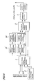
- Figure 4 is a diagram showing configurations of a circuit to perform the level monitoring process and weighing coefficient control process after correlation value calculation. As shown in Fig. 4, between a correlation value calculating section 1 and an in-phase component adding section 3, a power level change monitoring section 15, a weighing coefficient controlling section 16, a power level change monitoring section 25, and a weighing coefficient controlling section 26 are connected. Moreover, same reference numbers are assigned to components having same functions as those shown in Fig. 1 and their descriptions are omitted accordingly.
- a change in correlation value level of each of an I component correlation value and a Q component correlation value is checked.
- a weighing coefficient is determined from the result and weighing control is exercised at time of an in-phase component adding calculating process by the in-phase component adding section 3 to obtain a result from the in-phase component adding calculation in which an influence caused by noises is reduced.
- the weighing control may be exercised at time of the powering processing by a powering section 4.
- Figure 5 is a diagram showing configurations of a circuit to perform the level monitoring process and weighing coefficient control process after the in-phase component adding processing. As shown in Fig. 5, between an in-phase correlation value calculating section 3 and a powering section 4, a power level change monitoring section 35, a weighing coefficient controlling section 36, a power level change monitoring section 45, and a weighing coefficient controlling section 46 are connected. Moreover, same reference numbers are assigned to components having same functions as those shown in Fig. 1 and their descriptions are omitted accordingly.
- a change in correlation value levels of each of the I component correlation value and the Q component correlation value is checked.
- a weighing coefficient is determined from the result and weighing control is exercised at time of a powering process by the powering section 4 to obtain a result from the in-phase component adding calculation in which an influence by noises is reduced.
- a first method is to fix a value, in advance, as the threshold value.
- a second method is to determine the threshold value based on a fed-back maximum power level by using average profiles in the past. For example, a value of a maximum power level + xdB ("x" may be a negative value) or a like can be used.
- a third method is to determine the threshold value based on a maximum power level detected in same delay profiles. For example, a value of a maximum power level + xdB ("x" may be a negative value) or a like can be used.
- a path searching program which has a computer (controlling section 8) execute the path searching method described in the first and second examples.
- the path searching program is stored in the storage medium 9 shown in Fig. 1. Contents of the path searching program is shown in the flowchart shown in Fig. 3.
- the controlling section 8 controls the power level change monitoring sections 5, 15, 25, 35, and 45 and weighing coefficient controlling sections 6, 16, 26, 36, and 46 in accordance with the path searching program stored in the storage medium 9. Descriptions of contents of the path searching program are omitted accordingly.
- a path searching circuit which is capable of searching a stable path.
- a power delay profile calculated by a powering section (4) using an I component correlation value and a Q component correlation value is input to a power level change monitoring section (5), where a change in a power level is monitored at a sampling point for each of two or more delay profiles to be used for same power adding processing.
- a power level change monitoring section (5) where a change in a power level is monitored at a sampling point for each of two or more delay profiles to be used for same power adding processing.
Landscapes
- Engineering & Computer Science (AREA)
- Computer Networks & Wireless Communication (AREA)
- Signal Processing (AREA)
- Mobile Radio Communication Systems (AREA)
- Cable Transmission Systems, Equalization Of Radio And Reduction Of Echo (AREA)
Applications Claiming Priority (2)
| Application Number | Priority Date | Filing Date | Title |
|---|---|---|---|
| JP2003019604 | 2003-01-29 | ||
| JP2003019604A JP4165238B2 (ja) | 2003-01-29 | 2003-01-29 | パスサーチ回路及びその方法ならびにプログラム |
Publications (3)
| Publication Number | Publication Date |
|---|---|
| EP1443672A2 true EP1443672A2 (fr) | 2004-08-04 |
| EP1443672A3 EP1443672A3 (fr) | 2005-01-05 |
| EP1443672B1 EP1443672B1 (fr) | 2007-08-01 |
Family
ID=32652858
Family Applications (1)
| Application Number | Title | Priority Date | Filing Date |
|---|---|---|---|
| EP20040001943 Expired - Lifetime EP1443672B1 (fr) | 2003-01-29 | 2004-01-29 | Procédé, appareil et programme de détermination de chemins |
Country Status (5)
| Country | Link |
|---|---|
| US (1) | US7804810B2 (fr) |
| EP (1) | EP1443672B1 (fr) |
| JP (1) | JP4165238B2 (fr) |
| CN (1) | CN1277362C (fr) |
| DE (1) | DE602004007834T2 (fr) |
Families Citing this family (8)
| Publication number | Priority date | Publication date | Assignee | Title |
|---|---|---|---|---|
| US20060067383A1 (en) * | 2004-09-29 | 2006-03-30 | Carmela Cozzo | Parameter estimate initialization using interpolation |
| CN1707989B (zh) * | 2005-05-13 | 2010-12-22 | 上海宣普实业有限公司 | 码分多址系统中定时跟踪的路径搜索方法 |
| JP4728772B2 (ja) * | 2005-10-26 | 2011-07-20 | 日本電気株式会社 | 遅延プロファイル生成回路及びその方法並びにそれを用いた受信機、プログラム |
| US8014478B2 (en) * | 2007-12-26 | 2011-09-06 | Broadcom Corporation | Method and apparatus for impulse noise detection and suppression for DVB-T |
| US20110026430A1 (en) * | 2009-07-30 | 2011-02-03 | Qualcomm Incorporated | Method and apparatus for detecting a channel condition for a wireless communication device |
| US9094083B2 (en) * | 2010-05-18 | 2015-07-28 | Qualcomm Incorporated | Systems, apparatus and methods to facilitate efficient repeater usage |
| JP5896795B2 (ja) * | 2012-03-14 | 2016-03-30 | 三菱電機株式会社 | 等化装置、受信装置及び等化方法 |
| US9383437B2 (en) | 2013-04-10 | 2016-07-05 | Mitsubishi Electric Corporation | Reception device and reception method |
Family Cites Families (35)
| Publication number | Priority date | Publication date | Assignee | Title |
|---|---|---|---|---|
| JP2934185B2 (ja) * | 1996-03-15 | 1999-08-16 | 松下電器産業株式会社 | Cdmaセルラ無線基地局装置および移動局装置および送信方法 |
| US6026115A (en) * | 1996-08-23 | 2000-02-15 | Ntt Mobile Communications Network, Inc. | Rake receiver |
| JP2924864B2 (ja) * | 1997-06-16 | 1999-07-26 | 日本電気株式会社 | 適応レイク受信方式 |
| US6731711B1 (en) * | 1997-11-19 | 2004-05-04 | Lg Electronics Inc. | Signal recovery system |
| DE19824218C1 (de) | 1998-05-29 | 2000-03-23 | Ericsson Telefon Ab L M | Multipfad-Ausbreitungsverzögerungs-Bestimmungsvorrichtung unter Verwendung von periodisch eingefügten Pilotsymbolen |
| JP3092798B2 (ja) * | 1998-06-30 | 2000-09-25 | 日本電気株式会社 | 適応送受信装置 |
| CA2302269C (fr) * | 1998-07-16 | 2003-11-04 | Samsung Electronics Co., Ltd. | Traitement de donnees en paquets, dans un systeme de communication mobile |
| JP3031354B1 (ja) * | 1998-09-30 | 2000-04-10 | 日本電気株式会社 | Cdma受信装置及びそのマルチパスのフィンガ割り当て方法並びにその制御プログラムを記録した記録媒体 |
| JP3554207B2 (ja) * | 1998-11-10 | 2004-08-18 | 松下電器産業株式会社 | 無線通信装置及び無線通信方法 |
| US6269239B1 (en) * | 1998-12-11 | 2001-07-31 | Nortel Networks Corporation | System and method to combine power control commands during soft handoff in DS/CDMA cellular systems |
| JP3641961B2 (ja) * | 1999-02-01 | 2005-04-27 | 株式会社日立製作所 | アダプティブアレイアンテナを使用した無線通信装置 |
| JP3149868B2 (ja) * | 1999-02-24 | 2001-03-26 | 日本電気株式会社 | Cdma受信装置の受信パス・サーチ方法およびサーチャー回路 |
| JP2000252955A (ja) | 1999-03-02 | 2000-09-14 | Sanyo Electric Co Ltd | 受信装置及び受信方法 |
| JP3930187B2 (ja) * | 1999-03-03 | 2007-06-13 | 株式会社日立コミュニケーションテクノロジー | 同期制御方法、受信機、基地局及び移動端末 |
| JP3322246B2 (ja) | 1999-07-21 | 2002-09-09 | 日本電気株式会社 | パスサーチ装置および方法 |
| US6996080B1 (en) * | 1999-07-23 | 2006-02-07 | Itt Manufacturing Enterprises, Inc. | Chip-synchronous CDMA multiplexer and method resulting in constant envelope signals |
| KR20010038528A (ko) * | 1999-10-26 | 2001-05-15 | 조정남 | 부호분할 다중접속 시스템에서의 역방향 링크의 전력 제어 장치 및 방법 |
| US7072381B2 (en) * | 1999-12-28 | 2006-07-04 | Ntt Docomo, Inc. | Path search method, channel estimation method and communication device |
| JP2001203620A (ja) * | 2000-01-19 | 2001-07-27 | Matsushita Electric Ind Co Ltd | 無線基地局装置及び無線通信方法 |
| WO2001067627A1 (fr) * | 2000-03-06 | 2001-09-13 | Fujitsu Limited | Recepteur amcr et detecteur d'un tel recepteur |
| JP2001308744A (ja) * | 2000-04-19 | 2001-11-02 | Nec Corp | 移動通信復調装置及びその復調方法並びにその制御プログラムを記録した記録媒体 |
| JP3501783B2 (ja) * | 2000-08-23 | 2004-03-02 | 日本電気株式会社 | Cdma受信装置およびcdma受信方法 |
| JP3497480B2 (ja) * | 2000-09-04 | 2004-02-16 | 松下電器産業株式会社 | 位相回転検出装置及びそれを備えた無線基地局装置 |
| JP2002198875A (ja) * | 2000-12-22 | 2002-07-12 | Nippon Soken Inc | Cdma方式の通信端末 |
| JP4081982B2 (ja) | 2001-01-30 | 2008-04-30 | 日本電気株式会社 | Cdma移動通信復調回路及び復調方法 |
| JP3551254B2 (ja) | 2001-02-05 | 2004-08-04 | 日本電気株式会社 | パス検出方法、パス検出装置及びアレーアンテナ受信装置 |
| JP3676986B2 (ja) * | 2001-03-29 | 2005-07-27 | 松下電器産業株式会社 | 無線受信装置及び無線受信方法 |
| JP3558053B2 (ja) * | 2001-06-06 | 2004-08-25 | 日本電気株式会社 | 適応アンテナ受信装置 |
| GB2384660B (en) * | 2002-01-25 | 2004-11-17 | Toshiba Res Europ Ltd | Reciever processing systems |
| US6748009B2 (en) * | 2002-02-12 | 2004-06-08 | Interdigital Technology Corporation | Receiver for wireless telecommunication stations and method |
| US6748013B2 (en) * | 2002-02-12 | 2004-06-08 | Interdigital Technology Corporation | Receiver for wireless telecommunication stations and method |
| WO2004025859A1 (fr) * | 2002-09-13 | 2004-03-25 | Telefonaktiebolaget Lm Ericsson (Publ) | Procede de programmation d'un dispositif de recherche de chemins |
| US20040072553A1 (en) * | 2002-09-20 | 2004-04-15 | Xiaohui Wang | Methods, systems, and computer program products for selecting delay positions for a RAKE receiver by adjusting the delay positions based on comparisons of signal to interference ratios and/or powers for multi-path signals over time |
| JP3969275B2 (ja) * | 2002-10-15 | 2007-09-05 | 株式会社日立製作所 | 無線位置測定方法および装置 |
| US7277474B2 (en) * | 2002-11-05 | 2007-10-02 | Analog Devices, Inc. | Finger allocation for a path searcher in a multipath receiver |
-
2003
- 2003-01-29 JP JP2003019604A patent/JP4165238B2/ja not_active Expired - Fee Related
-
2004
- 2004-01-28 US US10/765,124 patent/US7804810B2/en not_active Expired - Fee Related
- 2004-01-29 CN CNB2004100074124A patent/CN1277362C/zh not_active Expired - Fee Related
- 2004-01-29 DE DE200460007834 patent/DE602004007834T2/de not_active Expired - Lifetime
- 2004-01-29 EP EP20040001943 patent/EP1443672B1/fr not_active Expired - Lifetime
Also Published As
| Publication number | Publication date |
|---|---|
| JP4165238B2 (ja) | 2008-10-15 |
| CN1520079A (zh) | 2004-08-11 |
| DE602004007834D1 (de) | 2007-09-13 |
| EP1443672B1 (fr) | 2007-08-01 |
| EP1443672A3 (fr) | 2005-01-05 |
| JP2004235777A (ja) | 2004-08-19 |
| US7804810B2 (en) | 2010-09-28 |
| US20040184411A1 (en) | 2004-09-23 |
| CN1277362C (zh) | 2006-09-27 |
| DE602004007834T2 (de) | 2008-04-10 |
Similar Documents
| Publication | Publication Date | Title |
|---|---|---|
| EP1065801B1 (fr) | Recherche adaptative de voies dans un récepteur amrc | |
| US6370183B1 (en) | Predictive rake receiver for CDMA mobile radio systems | |
| KR100384097B1 (ko) | 개선된 경로 타이밍 검출 방법 및 그것을 이용한 cdma수신 장치 | |
| JPH0879146A (ja) | ダイバーシチ受信装置 | |
| JP2002520982A (ja) | Ds−cdma受信機のための経路選択しきい値の適応設定方法 | |
| JP3943062B2 (ja) | Cdma受信装置、cdma受信方法、cdma受信プログラム、及び、プログラム記録媒体 | |
| US7804810B2 (en) | Circuit, method, and program in a CDMA communication system for quickly tracking a stable path | |
| KR0154706B1 (ko) | 부호분할 다중접속 방식 통신 시스템의 역방향 통화채널에서의 다중경로 지연시간 탐색기 | |
| CN100518032C (zh) | Cdma解调电路和解调方法 | |
| KR20080060297A (ko) | 신호 경로 집중에 기초한 레이크 수신기 핑거 할당 | |
| US7039099B2 (en) | Demodulation apparatus and demodulation method for mobile communication | |
| JP2003158474A (ja) | Cdma受信装置と、その基地局、及びその受信信号を逆拡散するための受信タイミングの検出方法 | |
| CN115226197B (zh) | 无线通信的帧定时同步方法、装置、电子设备 | |
| JP4081982B2 (ja) | Cdma移動通信復調回路及び復調方法 | |
| JPH1117649A (ja) | Rake合成パス検出方式およびrake合成パス検出回路 | |
| US7269437B2 (en) | Transmission power control circuit using W-CDMA method | |
| EP1154585B1 (fr) | Récepteur pour un dispositif de communication pour un canal radio à multi-voies | |
| KR20010085631A (ko) | 통신 단말 장치 및 셀 탐색 방법 | |
| KR100493072B1 (ko) | 다중 경로 채널상에서 코드 동기 획득을 위한 적응 임계값결정 방법 및 장치 | |
| EP1137193A2 (fr) | Procédé et circuit de mésure du profile de retard | |
| US20090073956A1 (en) | Path search processing circuit, path search method, and control program | |
| KR100287914B1 (ko) | 고성능 신호 검색 정렬 장치 및 방법 | |
| Jouini et al. | A New Methodology Of Auto-Adaptive PN Code Acquisition For Spread Spectrum Communications Environment | |
| JP2005354263A (ja) | 受信装置及び受信装置におけるパス選択方法 | |
| JP2001274726A (ja) | スペクトラム拡散受信装置及びスペクトラム拡散受信方法 |
Legal Events
| Date | Code | Title | Description |
|---|---|---|---|
| PUAI | Public reference made under article 153(3) epc to a published international application that has entered the european phase |
Free format text: ORIGINAL CODE: 0009012 |
|
| AK | Designated contracting states |
Kind code of ref document: A2 Designated state(s): AT BE BG CH CY CZ DE DK EE ES FI FR GB GR HU IE IT LI LU MC NL PT RO SE SI SK TR |
|
| AX | Request for extension of the european patent |
Extension state: AL LT LV MK |
|
| PUAL | Search report despatched |
Free format text: ORIGINAL CODE: 0009013 |
|
| AK | Designated contracting states |
Kind code of ref document: A3 Designated state(s): AT BE BG CH CY CZ DE DK EE ES FI FR GB GR HU IE IT LI LU MC NL PT RO SE SI SK TR |
|
| AX | Request for extension of the european patent |
Extension state: AL LT LV MK |
|
| 17P | Request for examination filed |
Effective date: 20050616 |
|
| AKX | Designation fees paid |
Designated state(s): DE FR GB IT |
|
| GRAP | Despatch of communication of intention to grant a patent |
Free format text: ORIGINAL CODE: EPIDOSNIGR1 |
|
| GRAS | Grant fee paid |
Free format text: ORIGINAL CODE: EPIDOSNIGR3 |
|
| GRAA | (expected) grant |
Free format text: ORIGINAL CODE: 0009210 |
|
| AK | Designated contracting states |
Kind code of ref document: B1 Designated state(s): DE FR GB IT |
|
| REG | Reference to a national code |
Ref country code: GB Ref legal event code: FG4D |
|
| REF | Corresponds to: |
Ref document number: 602004007834 Country of ref document: DE Date of ref document: 20070913 Kind code of ref document: P |
|
| ET | Fr: translation filed | ||
| PLBE | No opposition filed within time limit |
Free format text: ORIGINAL CODE: 0009261 |
|
| STAA | Information on the status of an ep patent application or granted ep patent |
Free format text: STATUS: NO OPPOSITION FILED WITHIN TIME LIMIT |
|
| 26N | No opposition filed |
Effective date: 20080506 |
|
| REG | Reference to a national code |
Ref country code: FR Ref legal event code: TP Owner name: WARREN & LEWIS INVESTMENT CORPORATION, US Effective date: 20130102 |
|
| REG | Reference to a national code |
Ref country code: GB Ref legal event code: 732E Free format text: REGISTERED BETWEEN 20130110 AND 20130116 |
|
| PGFP | Annual fee paid to national office [announced via postgrant information from national office to epo] |
Ref country code: DE Payment date: 20130731 Year of fee payment: 10 |
|
| REG | Reference to a national code |
Ref country code: DE Ref legal event code: R082 Ref document number: 602004007834 Country of ref document: DE Representative=s name: PATENTANWAELTE BETTEN & RESCH, DE Effective date: 20130912 Ref country code: DE Ref legal event code: R081 Ref document number: 602004007834 Country of ref document: DE Owner name: WARREN & LEWIS INVESTMENT CORPORATION, US Free format text: FORMER OWNER: NEC CORP., TOKYO, JP Effective date: 20130912 Ref country code: DE Ref legal event code: R081 Ref document number: 602004007834 Country of ref document: DE Owner name: WARREN & LEWIS INVESTMENT CORPORATION, FALLS C, US Free format text: FORMER OWNER: NEC CORP., TOKYO, JP Effective date: 20130912 |
|
| PGFP | Annual fee paid to national office [announced via postgrant information from national office to epo] |
Ref country code: FR Payment date: 20130730 Year of fee payment: 10 Ref country code: GB Payment date: 20130709 Year of fee payment: 10 |
|
| PGFP | Annual fee paid to national office [announced via postgrant information from national office to epo] |
Ref country code: IT Payment date: 20130715 Year of fee payment: 10 |
|
| REG | Reference to a national code |
Ref country code: DE Ref legal event code: R119 Ref document number: 602004007834 Country of ref document: DE |
|
| GBPC | Gb: european patent ceased through non-payment of renewal fee |
Effective date: 20140129 |
|
| REG | Reference to a national code |
Ref country code: DE Ref legal event code: R119 Ref document number: 602004007834 Country of ref document: DE Effective date: 20140801 |
|
| PG25 | Lapsed in a contracting state [announced via postgrant information from national office to epo] |
Ref country code: DE Free format text: LAPSE BECAUSE OF NON-PAYMENT OF DUE FEES Effective date: 20140801 |
|
| REG | Reference to a national code |
Ref country code: FR Ref legal event code: ST Effective date: 20140930 |
|
| PG25 | Lapsed in a contracting state [announced via postgrant information from national office to epo] |
Ref country code: FR Free format text: LAPSE BECAUSE OF NON-PAYMENT OF DUE FEES Effective date: 20140131 Ref country code: GB Free format text: LAPSE BECAUSE OF NON-PAYMENT OF DUE FEES Effective date: 20140129 |
|
| PG25 | Lapsed in a contracting state [announced via postgrant information from national office to epo] |
Ref country code: IT Free format text: LAPSE BECAUSE OF NON-PAYMENT OF DUE FEES Effective date: 20140129 |