EP1445864A2 - Elément logique et procédé associé - Google Patents
Elément logique et procédé associé Download PDFInfo
- Publication number
- EP1445864A2 EP1445864A2 EP04250564A EP04250564A EP1445864A2 EP 1445864 A2 EP1445864 A2 EP 1445864A2 EP 04250564 A EP04250564 A EP 04250564A EP 04250564 A EP04250564 A EP 04250564A EP 1445864 A2 EP1445864 A2 EP 1445864A2
- Authority
- EP
- European Patent Office
- Prior art keywords
- multiplexer
- multiplexers
- inputs
- logic element
- lut
- Prior art date
- Legal status (The legal status is an assumption and is not a legal conclusion. Google has not performed a legal analysis and makes no representation as to the accuracy of the status listed.)
- Withdrawn
Links
Images


Classifications
-
- H—ELECTRICITY
- H03—ELECTRONIC CIRCUITRY
- H03K—PULSE TECHNIQUE
- H03K19/00—Logic circuits, i.e. having at least two inputs acting on one output; Inverting circuits
- H03K19/02—Logic circuits, i.e. having at least two inputs acting on one output; Inverting circuits using specified components
- H03K19/173—Logic circuits, i.e. having at least two inputs acting on one output; Inverting circuits using specified components using elementary logic circuits as components
- H03K19/177—Logic circuits, i.e. having at least two inputs acting on one output; Inverting circuits using specified components using elementary logic circuits as components arranged in matrix form
- H03K19/17724—Structural details of logic blocks
- H03K19/17728—Reconfigurable logic blocks, e.g. lookup tables
-
- H—ELECTRICITY
- H03—ELECTRONIC CIRCUITRY
- H03K—PULSE TECHNIQUE
- H03K19/00—Logic circuits, i.e. having at least two inputs acting on one output; Inverting circuits
- H03K19/02—Logic circuits, i.e. having at least two inputs acting on one output; Inverting circuits using specified components
- H03K19/173—Logic circuits, i.e. having at least two inputs acting on one output; Inverting circuits using specified components using elementary logic circuits as components
- H03K19/1733—Controllable logic circuits
- H03K19/1737—Controllable logic circuits using multiplexers
Definitions
- the present invention relates to a logic element and a method of manufacturing a logic element.
- the logic element has particular though not exclusive application for use with programmable logic devices or other similar devices.
- PLDs Programmable logic devices
- CPLDs CPLDs
- PALs PLAs
- PLAs PLAs
- FPLAs FPLAs
- EPLDs EEPLDs
- LCAs LCAs
- FPGAs FPGAs
- PLDs Programmable logic devices
- Such devices are well known in the art and typically provide an "off the shelf” device having at least a portion that can be electrically programmed to meet a user's specific needs.
- ASICs Application specific integrated circuits
- PLD as used herein will be considered broad enough to include such devices.
- PLDs typically include blocks of logic elements, which are sometimes referred to as logic array blocks (“LABs”) or “configurable logic blocks” (“CLBs”).
- Logic elements which are also referred to by other names such as “logic circuits” or “logic cells”, may include a look-up table (“LUT”), product term, carry-out chain, register, and other elements.
- Logic elements typically include configurable elements holding configuration data that determine the particular function or functions carried out by the logic element.
- a typical LUT circuit may include RAM bits that hold data (a "1" or “0").
- Other types of configurable elements may be used. Some examples may include static, magnetic, ferroelectric or dynamic random access memory, electrically erasable read-only memory, flash, fuse, and anti-fuse programmable connections.
- the programming of configuration elements could also be implemented through mask programming during fabrication of the device. While mask programming may have disadvantages relative to some of the field programmable options already listed, it may be useful in certain high volume applications.
- the generic term "memory element" will be used to refer to any programmable element that may be configured to determine functions implemented by a PLD.
- K-LUT K-input lookup table
- K-LUT typically includes 2 K programmable memory elements, and a 2 K to 1 multiplexer, selecting one of the storage elements under the control of the K select inputs to the multiplexer.
- K inputs can be considered to be the inputs to a K-input logic function which can implement any particular required logic function by setting the contents of the memory elements to the appropriate values.
- the 6-LUT circuitry are offset by a reduction in the delay.
- the longest path through a logic circuit might be ten 4-LUTs versus eight 6-LUTs.
- the 6-LUT version of the circuit might be larger, but faster.
- the 6-LUT circuit would likely require less programmable routing in a PLD, offsetting some of its higher cost.
- the eight-hundred 6-LUTs might actually include three-hundred 6-input functions, three-hundred 5-input functions, one-hundred 4-input functions, and one-hundred 3-input functions.
- the LE based on 6-LUTs is only being used to its fullest extent in three-hundred out of eight-hundred instances.
- a logic element comprising: a plurality of memory elements; a plurality of multiplexers arranged in a plurality of levels, each level including at least one multiplexer, the levels including a highest level of multiplexer with inputs connected to the memory elements and outputs connected to inputs of a next-to-highest level of multiplexer, and a first level of multiplexer with inputs connected to outputs of a second level of multiplexer and at least one output; and, a plurality of controls connected to the multiplexers; wherein: in a first operational mode the controls determine a first-mode output at the at least one output of the first level of multiplexer, and in a second operational mode the controls determine a plurality of second-mode outputs at selected outputs of multiplexers not at the first level of multiplexer.
- a method of making a logic element comprising: providing a plurality of memory elements; providing a plurality of multiplexers, the multiplexers being arranged in a plurality of levels, each level including at least one multiplexer, the levels including a highest level of multiplexer with inputs connected to the memory elements and outputs connected to inputs of a next-to-highest level of multiplexer, and a first level of multiplexer with inputs connected to outputs of a second level of multiplexer and at least one output; and, providing a plurality of controls, the controls being connected to the multiplexers, wherein: in a first operational mode the controls determine a first-mode output at the at least one output of the first level of multiplexer, and in a second operational mode the controls determine a plurality of second-mode outputs at selected outputs of multiplexers not at the first level of multiplexer.
- a logic element includes memory elements, multiplexers, and controls.
- the multiplexers are arranged in levels including a highest level of multiplexers with inputs connected to the memory elements and outputs connected to inputs of a next-to-highest level of multiplexers and a first level of multiplexers with inputs connected to outputs of a second level of multiplexers and at least one output.
- the controls are connected to the multiplexers. In a first operational mode the controls determine a first-mode output at the at least one output of the first level of multiplexers, and in a second operational mode the controls determine second-mode outputs at selected outputs of multiplexers not at the first level of multiplexers.
- the logic element when the logic element is in the first operational mode, the first-mode output provides a complete function of the controls. According to another aspect, when the logic element is in the second operational mode, each second-mode output provides a complete function of a proper subset of the controls. According to another aspect, when the logic element is in the second operational mode, one or more controls are split into sub-controls so that a corresponding sub-control replaces each split control at each multiplexer connected to that split control. According to another aspect, the logic element further includes one or more control multiplexers with outputs connected to one or more of the controls of the logic element and with inputs determined by control-multiplexer inputs. Under some operational conditions, at least two of the control multiplexers receive an identical control-multiplexer input.
- the logic element further includes additional multiplexers that can be combined with flip-flops.
- the logic element further includes one or more mode multiplexers connected to the logic element for switching between the first operational mode and the second operational mode.
- the logic element is included in a programmable logic device, which itself may be included in a data processing system.
- a method of making a logic element includes providing memory elements, providing multiplexers, and providing controls.
- the multiplexers are arranged in levels including a highest level of multiplexers with inputs connected to the memory elements and outputs connected to inputs of a next-to-highest level of multiplexers and a first level of multiplexers with inputs connected to outputs of a second level of multiplexers and at least one output.
- the controls are connected to the multiplexers. In a first operational mode the controls determine a first-mode output at the at least one output of the first level of multiplexers, and in a second operational mode the controls determine second-mode outputs at selected outputs of multiplexers not at the first level of multiplexers.
- the method further includes adding to the logic element one or more control multiplexers with outputs connected to one or more of the controls of the logic element and with inputs determined by control-multiplexer inputs.
- the method further includes adding to the logic element one or more mode multiplexers connected to the logic element for switching between the first operational mode and the second operational mode.
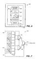
- Figure 7 shows a conventional 6-LUT 700 that includes four 4-LUTs 702.
- Each 4-LUT 702 includes sixteen memory elements and a 16:1 multiplexer that is controlled by inputs a, b, c, and d 704.
- Outputs from the 4-LUTs 702 provide inputs to two 2:1 multiplexers 706, each of which is controlled by input e 708.
- Outputs from these multiplexers provide inputs to an additional 2:1 multiplexer 710 that is controlled by input f 712 to provide a final output 714. In this way any function of six inputs z1(a,b,c,d,e,f) can be implemented.
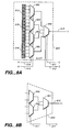
- FIG 8A shows a conventional 4-LUT 800, which could be used as a component of the 6-LUT shown in Figure 7.
- the 4-LUT 800 includes memory elements 819, and 4:1 multiplexers 850, 840.
- Each memory element 819 can hold one data bit (i.e., 1 or 0) and each is coupled to provide that bit to an input of a multiplexer 850 as shown.
- Two control inputs of each multiplexer 850 are coupled to, respectively, an input A 814 and an input B 813 of the 4-LUT 800.
- the output of each of these multiplexers 850 is coupled to an input of another 4:1 multiplexer 840 as shown.
- Two control inputs of this multiplexer 840 are coupled to, respectively, an input C 811 and an input D 812 of the 4-LUT 800.
- the output of this multiplexer 840 provides the final output 815 of the 4-LUT 800.
- a 4-LUT such as the 4-LUT 800 of Figure 8A can provide a complete function of four input signals.
- “Complete" in this context simply means that the memory elements 819 can be programmed to configure the 4-LUT 800 to perform any four-input function. That is, the 4-LUT 800 can be configured by programming its memory elements (e.g., loading values into those elements) so that the output signal Y 815 is any one of a full range of logical functions of the input signals A 814, B 813, C 811 and D 812 as will be appreciated by those skilled in the art.
- the 6-LUT of Figure 7 also provides a complete function of its six input signals.
- Figure 8B illustrates the "tree" of 2:1 multiplexers 841, 842 that make up the final 4:1 multiplexer 840.
- the other 4:1 multiplexers 850 can be similarly characterised.
- Control inputs 811, 812 of the multiplexers 841, 842 correspond to inputs of the 4-LUT 800.
- An output at a higher level of multiplexers 842 i.e., closer to the memory elements 819) feeds into the next level 841 closer to the output 815.
- the "tree" of the 2:1 multiplexers 841, 842 making up the final 4:1 multiplexer 840 as part of a larger 2:1 multiplexer tree that characterises the 4-LUT 800.
- a typical LUT circuit has a multiplexer tree that may be referenced by "levels" of 2:1 multiplexers provided relative to the LUT circuit's output.
- the multiplexer 841 closest to the output 815 may be called a first level of multiplexers in the overall 2:1 multiplexer tree of the 4-LUT 800 and the next set of two multiplexers 842 may be called a second level in that tree.
- the 4-LUT 800 has a third level that includes four 2:1 multiplexers (i.e., one for each multiplexer 850) with control inputs coupled to logic input B 813, and a fourth level that includes eight 2:1 multiplexers (i.e., two for each multiplexer 850) with control inputs coupled to logic input A 114.
- a 4:1 multiplexer may be implemented in a manner other than the illustrated multiplexer 840, which has a "tree" of three 2:1 multiplexers 841, 842 at two distinct levels.
- a 4:1 multiplexer might be implemented by four pass gates with each of the pass gates being controlled by the decoded output of two control signals. In such an example, the four pass gates themselves would not be differentiated by levels relative to each other. However, the 4:1 multiplexer would effectively implement two levels of 2:1 multiplexing.
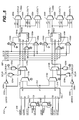
- FIG. 1 shows an example of a fracturable 6-LUT 100 according to an embodiment of the present invention.
- the fracturable 6-LUT 100 includes four 4-LUTs 102.
- Each 4-LUT 102 includes sixteen memory elements and a 16:1 multiplexer that is controlled by inputs a, b, c, and d 104.
- Outputs from the 4-LUTs 102 provide inputs to two 2:1 multiplexers 106, each of which is controlled by input e 108.
- Outputs from these multiplexers 106 provide inputs to an additional 2:1 multiplexer 110 that is controlled by input f 112 to provide a final output 114.
- any function of six inputs z1(a,b,c,d,e,f) can be implemented.
- the fracturable 6-LUT 100 includes an additional 2:1 multiplexer 116 that takes inputs from two of the 4-LUTs 102 and is controlled by input f 112.
- the output signal z1 114 is a complete function of all 6 inputs.
- the output z0 118 which is taken from the top half of the LUT 100 provides a complete function of a,b,c,d,e and the output z2 120, taken from the extra 2:1 multiplexer 116, provides a complete function of a,b,c,d,f.
- the LUT can implement two 5-input functions that share the four inputs a, b, c, and d.
- Logic external to the fracturable LUT is used to select between the z1 function 114 when the LUT 100 is used as a single 6-LUT, or the z0 118 and z2 120 outputs when the LUT 100 is used as two 5-LUTs. It can be appreciated that it is possible to continue the fracturing of the LUT further, so that for example a fracturable 6-LUT could be configured as a combination of one 5-LUT and two 4-LUTs.
- a fracturable K-LUT has only K inputs, so that the two (K-1) functions must use a common set of K input signals.
- each (K-1)-LUT has only one unique input signal, and shares (K-2) signals with another LUT.
- K,M fracturable
- FIG. 2 shows an example of a fracturable (6,2)-LUT according to an embodiment of the present invention.
- the fracturable (6,2)-LUT 200 includes four 4-LUTs 202.
- Each 4-LUT 202 includes sixteen memory elements and a 16:1 multiplexer.
- Outputs from the 4-LUTs 202 provide inputs to two 2:1 multiplexers 206, each of which is controlled by input e 208.
- Outputs from these multiplexers 206 provide inputs to an additional 2:1 multiplexer 210 that is controlled by input f 212 to provide a final output 214.
- An additional 2:1 multiplexer 216 takes inputs from two of the 4-LUTs 202 and is controlled by input f 212.
- two of the inputs to the four 4-LUTs 202 are split. That is, two inputs a and b 204 correspond to similar inputs 104 in the fracturable 6-LUT 100. However, inputs c and d (corresponding generally to inputs c and d 104 of the fracturable 6-LUT 100) are split into inputs c1 and d1 222 for the upper half of the 4-LUTs 202 and inputs c2 and d2 224 for the lower half.
- the inputs to the LUT are listed (i.e., a, b, c, d) in order from slowest to fastest, so that the d is the fastest input to each of the 4-LUTs 202. It is desirable to split the fastest inputs to the LUT so that the fastest inputs are independent from each other.
- the top two 4-LUTs form a logic function z0 (a, b, c1, d1, e) and the bottom two 4-LUTs form a logic function z2(a,b,c2,d2,f).
- a and b must be shared between the two LUTs.
- the fracturable (6,2)-LUT 200 can implement any two functions that use no more than eight distinct input signals, such as a 3-input function and a 5-input function, by configuring the LUT to have no functional dependency on one or more of its inputs.
- the (6,2)-LUT 200 can implement functions z0 (c1, d1, e) 218 and z2(a,b,c2,d2,f) 220 by configuring the top half of the 4-LUTs 202 to have no dependency on inputs a and b 204.
- a (K,M)-LUT can implement any two functions of up to K-1 inputs that have no more than K+M distinct input signals.
- the fracturable (6,2)-LUT 200 may also be used for incomplete logic functions by using the eight inputs a, b, c1, c2, d1, d2, e, and f 208, 222, 204, 224, 212 together with the output at z1 214.
- some set of 8-input functions z1 (a,b,c1,c2,d1,d2,e,f) can be implemented, but, unlike a general LUT, not every 8-input function can be implemented. However, this may be exploited by attempting to design logic circuits that contain these functions as well as arbitrary functions.
- a logic element Another aspect of a logic element is the ability to feed a flip-flop from the LUT.
- the LUT output may be used as the data input to a flip-flop contained in the same logic element.
- the data input to the flip-flop may be selected to be one of the inputs to the LUT.
- a fracturable LUT is combined with one or more flip-flops in a logic element.
- FIG. 3 shows an example of a logic element 300 according to an embodiment of present invention.
- the logic element 300 includes a fracturable (6,2)-LUT 302 and two flip-flops 304a, 304b.
- the (6,2)-LUT 302 has inputs A, B, C1, C2, D1, D2, E, and F, where these are fed through input lines LEIMA, LEIMB, LEIMC1, LEIMC2, LEIMD1, LEIMD2, LEIME, and LEIMF 306. Additionally two multiplexers 308a, 308b feed inputs C1 and C2 by multiplexing LEIMC1 with a register value REG0 and by multiplexing LEIMC2 with a register value REG1.
- the LUT 302 provides a single output z1 310, and in a fractured mode the LUT 302 provides two outputs z0 123 and z1 314.
- the outputs from the LUT 302 are inputs to two multiplexers 316a, 316b. These multiplexers 316a, 316b provide input to another pair of multiplexers 318a, 318b that also take inputs from input lines LEIMC1 320a and LEIMC2 320b combined with circuitry of inverters 322a, 322b, NOR-gates 324a, 324b, and NAND-gates 326a, 326b.
- Output from these latter multiplexers 318a, 318b and line values LEIMC1 320a and LEIMC2 320b are fed to the flip-flops 304a, 304b, which also receive data from a combination of stored values 328 and multiplexers 330a, 330b.
- the structures associated with these flip-flops 304a, 304b are similar to those used in the Stratix logic element currently sold by Altera Corporation of San Jose, California.
- This logic element 300 desirably includes multiplexing structures for driving up to four signals out of the LE (i.e., LEOUTO, LEOUT1, LEOUT2, and LEOUT3) and two signals to internal routing (i.e., LOCAL0 and LOCAL1).
- the line signals LEIMx 306 refer to the sources of the logic signals connected to the inputs of the logic element.
- the embodiment of Figure 3 desirably includes two flip-flops 304a, 304b.
- the LUT 302 can now generate two logic functions, so it is desirable to have two flip-flops that can load data from the non-fractured K-LUT, or from either of the fractured LUTs.
- the flip-flop connectivity shown in Figure 3 can be generalised.
- the relevant flip-flop data input may be either the LUT output or in common with one of the LUT inputs.
- the arrangement of logic is similar to the Stratix logic element currently sold by Altera Corporation of San Jose, California.
- each of the flip-flops 304a, 304b can load from the 6-LUT output z1 310 or from one of the two 5-LUT outputs z0 312 and z2 314. Each output can select from the 6-LUT output, a 5-LUT output, or a flip-flop. Multiplexers are also provided to feed the flip-flop outputs back into the LUT to provide quick-feedback as in the Stratix device.
- the 6-LUT can feed one or both flip-flops, each 5-LUT can feed a flip-flop, or independent flip-flops may be combined with a 5-LUT that shares one input or a 4-LUT that does not share an input.
- FIG 4 shows another example of a logic element 400 according to an embodiment of present invention.
- This logic element 400 is similar to the logic element 300 of Figure 3 but includes additional multiplexing at the inputs to the LUT 402.
- Input line LEIMC1 406 and register value REG0 are inputs to a multiplexer 408a that feeds the C1 input of the LUT 402, and input lines LEIMC1 and LEIMC2 406 together with register value REG1 are inputs to a multiplexer 408b that feeds the C2 input of the LUT 402.
- the logic element 400 includes a fracturable (6,2)-LUT 402 and two flip-flops 404a, 404b.
- the (6,2)-LUT 402 has inputs A, B, C1, C2, D1, D2, E, and F, where these are fed through input lines LEIMA, LEIMB, LEIMC1, LEIMC2, LEIMD1, LEIMD2, LEIME, and LEIMF 406.
- two multiplexers 408a, 408b feed inputs C1 and C2 by multiplexing LEIMC1 with a register value REG0 and by multiplexing LEIMC2 with a register value REG1.
- the second multiplexer 408b which feeds input C2, receives input from input line LEIMC1, input line LEIMC2 and register value REG1.
- the LUT 402 provides a single output z1 410 in a non-fractured mode and two outputs, z0 412 and z1 414, in a fractured mode.
- the circuitry includes additional lines for LEMC1 420a and LEMC2 420b, multiplexers 416a, 416b, 418a, 418b, 430a, 430b, 432a, 432b, inverters 422a, 422b, NOR-gates 424a, 424b, NAND-gates 426a, 426b, stored values 428, and outputs 434a, 434b.
- the embodiment of Figure 4 advantageously exploits the additional input signals when the LUT 402 operates in the non-fractured mode.
- one of the extra inputs that resulted from splitting the original inputs (in this case C1) may be connected to its corresponding split input (in this case C2) at a corresponding multiplexer 408b.
- This allows the 6-LUT to bring the C signal on a single pin C1 and connect it to both C1 and C2 in the LUT 402.
- input pin C2 can now be used for another purpose, in this case to bring a data signal into a completely independent flip-flop 404b.
- This allows the logic element to support a 6-LUT that may optionally feed a flip-flop 404a, together with an independent flip-flop 404b.
- the 6-LUT can be used with quick feedback of the registers to the input of the LUT by using both flip-flops to load the identical data, so the result can be fed back to both C1 and C2.
- both REG0 and REG1 are input to either one or both of the multiplexers 408a, 408b feeding C1 and C1. This allows a single flip-flop to be used to store the data, and be fed back to both C1 and C2.
- the various alternatives differ in the choice of which flip-flops 404a, 404b can be used for quick feedback mode in the 6-LUT 402, and the optimal choice will depend on the logic circuits to be implemented and the flexibility of the routing structures provided in the PLD. Although it is generally preferable to feed the flip-flop with the slowest of the split inputs to the LUT, other inputs may be used as well.
- FIG. 5 shows another example of a logic element 500 according to an embodiment of present invention.
- This logic element 500 is similar to the logic element 300 of Figure 3 but includes additional multiplexing at the inputs to the LUT 502.
- Input line LEIMC1 506 feeds the C1 input of the LUT 502, and input lines LEIMC1 and LEIMC2 506 together with register value REG0 are inputs to a multiplexer 508a that feeds the C2 input of the LUT 502.
- Input line LEIMD2 506 feeds the D2 input of the LUT 502, and input lines LEIMD1 and LEIMD2 506 together with register value REG1 are inputs to a multiplexer 508b that feeds the D1 input of the LUT 502.
- the logic element 500 includes a fracturable (6,2)-LUT 502 and two flip-flops 504a, 504b.
- the (6,2)-LUT 502 has inputs A, B, C1, C2, D1, D2, E, and F, where these are fed through input lines LEIMA, LEIMB, LEIMC1, LEIMC2, LEIMD1, LEIMD2, LEIME, and LEIMF 506. Additionally two multiplexers 508a, 508b feed inputs C2 and D1 by multiplexing LEIMC1 and LEIMC2 with REG0 and by multiplexing LEIMD1 and LEIMD2 with REG1.
- the first multiplexer 508a which feeds input C2, receives input from input line LEIMC1, input line LEIMC2 and register value REG0
- the second multiplexer 408b which feeds input D1, receives input from input line LEIMD1, input line LEIMD2 and register value REG1.
- the LUT 502 provides a single output z1 510 in a non-fractured mode and two outputs, z0 512 and z2 514, in a fractured mode.
- the circuitry includes additional lines for LEMC1 520a and LEMC2 520b, multiplexers 516a, 516b, 518a, 518b, 530a, 530b, 532a, 532b, inverters 522a, 522b, NOR-gates 524a, 524b, NAND-gates 526a, 526b, stored values 528, and outputs 534a, 534b.
- the embodiment of Figure 5 enables increased flexibility by combining flip-flops 504a, 504b with LUTs so as to allow the 6-LUT 502 to be combined with two independent registers (REG0 at the first multiplexer 508a and REG1 at the second multiplexer 508b).
- REG0 at the first multiplexer 508a
- REG1 at the second multiplexer 508b
- C1 can be used as a LUT input and C2 as a data input to a flip-flop 504b
- D2 is used as another input to the LUT
- D1 as a data input to a flip-flop 504a.
- FIG. 6 shows an example of a data processing system 600 with a PLD 610 that may include embodiments of the present invention as discussed above.
- the PLD 610 includes a plurality of logic array blocks (LABs) such as the illustrated LAB 612. (Only one LAB is shown to avoid overcomplicating the drawing.)
- the LAB 612 includes a plurality of logic elements such as the illustrated logic element 611. (Only one logic element is shown to avoid overcomplicating the drawing.)
- the data processing system 600 may include one or more of the following components: a processor 640; memory 650; I/O circuitry 620; and peripheral devices 630. These components are coupled together by a system bus 665 and are populated on a circuit board 660 which is contained in an end-user system 670.
- the system 600 can be used in a wide variety of applications, such as computer networking, data networking, instrumentation, video processing, digital signal processing, or any other application where the advantage of using programmable or reprogrammable logic is desirable.
- the PLD 610 can be used to perform a variety of different logic functions.
- the PLD 610 can be configured as a processor or controller that works in cooperation with processor 640 (or, in alternative embodiments, a PLD might itself act as the sole system processor).
- the PLD 610 may also be used as an arbiter for arbitrating access to shared resources in the system 600.
- the PLD 610 can be configured as an interface between the processor 640 and one of the other components in system 600. It should be noted that system 600 is only exemplary.
Landscapes
- Physics & Mathematics (AREA)
- Mathematical Physics (AREA)
- Engineering & Computer Science (AREA)
- Computer Hardware Design (AREA)
- Computing Systems (AREA)
- General Engineering & Computer Science (AREA)
- Logic Circuits (AREA)
- Tests Of Electronic Circuits (AREA)
Applications Claiming Priority (2)
| Application Number | Priority Date | Filing Date | Title |
|---|---|---|---|
| US10/364,310 US6943580B2 (en) | 2003-02-10 | 2003-02-10 | Fracturable lookup table and logic element |
| US364310 | 2003-02-10 |
Publications (2)
| Publication Number | Publication Date |
|---|---|
| EP1445864A2 true EP1445864A2 (fr) | 2004-08-11 |
| EP1445864A3 EP1445864A3 (fr) | 2005-12-14 |
Family
ID=32655681
Family Applications (1)
| Application Number | Title | Priority Date | Filing Date |
|---|---|---|---|
| EP04250564A Withdrawn EP1445864A3 (fr) | 2003-02-10 | 2004-02-03 | Elément logique et procédé associé |
Country Status (4)
| Country | Link |
|---|---|
| US (3) | US6943580B2 (fr) |
| EP (1) | EP1445864A3 (fr) |
| JP (1) | JP4537086B2 (fr) |
| CN (3) | CN1540865B (fr) |
Cited By (3)
| Publication number | Priority date | Publication date | Assignee | Title |
|---|---|---|---|---|
| EP1770865A1 (fr) * | 2005-09-22 | 2007-04-04 | Altera Corporation | Une table de consultation fracturable pour des éléments logiques utilisant la surface de façon efficace |
| CN101312347B (zh) * | 2007-05-21 | 2014-09-03 | 阿尔特拉公司 | 具有复杂逻辑块的可编程逻辑器件 |
| US10229913B2 (en) | 2012-05-25 | 2019-03-12 | Semiconductor Energy Laboratory Co., Ltd. | Lookup table and programmable logic device including lookup table |
Families Citing this family (72)
| Publication number | Priority date | Publication date | Assignee | Title |
|---|---|---|---|---|
| US7800401B1 (en) | 2003-02-10 | 2010-09-21 | Altera Corporation | Fracturable lookup table and logic element |
| US6888373B2 (en) | 2003-02-11 | 2005-05-03 | Altera Corporation | Fracturable incomplete look up table for area efficient logic elements |
| US7302460B1 (en) * | 2003-09-11 | 2007-11-27 | Altera Corporation | Arrangement of 3-input LUT's to implement 4:2 compressors for multiple operand arithmetic |
| US7185035B1 (en) * | 2003-10-23 | 2007-02-27 | Altera Corporation | Arithmetic structures for programmable logic devices |
| US7167022B1 (en) | 2004-03-25 | 2007-01-23 | Altera Corporation | Omnibus logic element including look up table based logic elements |
| US7486110B2 (en) * | 2004-09-24 | 2009-02-03 | Stmicroelectronics Pvt. Ltd. | LUT based multiplexers |
| US7358765B2 (en) * | 2005-02-23 | 2008-04-15 | Cswitch Corporation | Dedicated logic cells employing configurable logic and dedicated logic functions |
| US7193436B2 (en) * | 2005-04-18 | 2007-03-20 | Klp International Ltd. | Fast processing path using field programmable gate array logic units |
| KR20060128450A (ko) * | 2005-06-10 | 2006-12-14 | 삼성전자주식회사 | 표시 장치 및 표시 장치의 구동 장치 |
| US7804719B1 (en) | 2005-06-14 | 2010-09-28 | Xilinx, Inc. | Programmable logic block having reduced output delay during RAM write processes when programmed to function in RAM mode |
| US7256612B1 (en) | 2005-06-14 | 2007-08-14 | Xilinx, Inc. | Programmable logic block providing carry chain with programmable initialization values |
| US7253658B1 (en) | 2005-06-14 | 2007-08-07 | Xilinx, Inc. | Integrated circuit providing direct access to multi-directional interconnect lines in a general interconnect structure |
| US7276934B1 (en) | 2005-06-14 | 2007-10-02 | Xilinx, Inc. | Integrated circuit with programmable routing structure including diagonal interconnect lines |
| US7268587B1 (en) | 2005-06-14 | 2007-09-11 | Xilinx, Inc. | Programmable logic block with carry chains providing lookahead functions of different lengths |
| US7274214B1 (en) | 2005-06-14 | 2007-09-25 | Xilinx, Inc. | Efficient tile layout for a programmable logic device |
| US7265576B1 (en) | 2005-06-14 | 2007-09-04 | Xilinx, Inc. | Programmable lookup table with dual input and output terminals in RAM mode |
| US7193433B1 (en) * | 2005-06-14 | 2007-03-20 | Xilinx, Inc. | Programmable logic block having lookup table with partial output signal driving carry multiplexer |
| US7375552B1 (en) | 2005-06-14 | 2008-05-20 | Xilinx, Inc. | Programmable logic block with dedicated and selectable lookup table outputs coupled to general interconnect structure |
| US7295035B1 (en) * | 2005-08-09 | 2007-11-13 | Lattice Semiconductor Corporation | Programmable logic device with enhanced logic block architecture |
| JP4438000B2 (ja) * | 2005-11-15 | 2010-03-24 | 株式会社半導体理工学研究センター | リコンフィギャラブルロジックブロック、リコンフィギャラブルロジックブロックを備えるプログラマブル論理回路装置、および、リコンフィギャラブルロジックブロックの構成方法 |
| US7902864B1 (en) * | 2005-12-01 | 2011-03-08 | Altera Corporation | Heterogeneous labs |
| US7420390B1 (en) * | 2006-01-09 | 2008-09-02 | Altera Corporation | Method and apparatus for implementing additional registers in field programmable gate arrays to reduce design size |
| US7262722B1 (en) * | 2006-06-26 | 2007-08-28 | Intel Corporation | Hardware-based CABAC decoder with parallel binary arithmetic decoding |
| US20080079460A1 (en) * | 2006-09-29 | 2008-04-03 | Infineon Technologies Ag | Programmable logic cell, configurable cell, configurable cell arrangement, configurable logic array, mask programmable basic cell, mask programmable gate array and method |
| US7459932B1 (en) * | 2007-05-24 | 2008-12-02 | Altera Corporation | Programmable logic device having logic modules with improved register capabilities |
| US7795913B2 (en) * | 2007-12-26 | 2010-09-14 | Tier Logic | Programmable latch based multiplier |
| US8514994B1 (en) | 2008-10-02 | 2013-08-20 | Altera Corporation | Double data rate operation in an integrated circuit |
| US7948792B1 (en) | 2009-04-15 | 2011-05-24 | Altera Corporation | Memory and techniques for using same |
| US7978102B1 (en) * | 2010-03-09 | 2011-07-12 | Himax Media Solutions, Inc. | Multi-bin CABAC decision bin decoder |
| JP5735503B2 (ja) | 2010-06-24 | 2015-06-17 | 太陽誘電株式会社 | 半導体装置 |
| JP5701054B2 (ja) * | 2010-12-28 | 2015-04-15 | 国立大学法人 熊本大学 | リコンフィギュラブルロジックブロック、並びに、これを用いたプログラマブル論理回路装置、及び、テクノロジマッピング方法 |
| CN102147720B (zh) * | 2011-03-18 | 2014-04-09 | 深圳市国微电子有限公司 | 用查找表实现多输入逻辑项之间的运算的装置及方法 |
| US9450585B2 (en) * | 2011-04-20 | 2016-09-20 | Microchip Technology Incorporated | Selecting four signals from sixteen inputs |
| CN103259528A (zh) * | 2012-02-17 | 2013-08-21 | 京微雅格(北京)科技有限公司 | 一种异构可编程逻辑结构的集成电路 |
| US8581624B2 (en) * | 2012-03-29 | 2013-11-12 | Altera Corporation | Integrated circuits with multi-stage logic regions |
| US20130278289A1 (en) * | 2012-04-18 | 2013-10-24 | Te-Tse Jang | Method and Apparatus for Improving Efficiency of Programmable Logic Circuit Using Cascade Configuration |
| US9007089B2 (en) * | 2012-10-21 | 2015-04-14 | Ememory Technology Inc. | Integrated circuit design protecting device and method thereof |
| US9350357B2 (en) | 2012-10-28 | 2016-05-24 | Taiyo Yuden Co., Ltd. | Reconfigurable semiconductor device |
| WO2014132670A1 (fr) * | 2013-03-01 | 2014-09-04 | アトナープ株式会社 | Dispositif et procédé de génération d'informations de reconfiguration |
| CN104242913B (zh) * | 2013-06-21 | 2018-01-05 | 京微雅格(北京)科技有限公司 | 一种面积优化的fpga互连结构 |
| CN103746686B (zh) * | 2014-01-26 | 2017-07-07 | 中国电子科技集团公司第五十八研究所 | 二维可扩展多路复用器的级联结构 |
| US9966960B2 (en) * | 2014-12-17 | 2018-05-08 | Silicon Laboratories Inc. | Configurable logic circuit including dynamic lookup table |
| US9705504B1 (en) * | 2016-01-13 | 2017-07-11 | Altera Corporation | Power gated lookup table circuitry |
| US10068045B1 (en) * | 2016-12-09 | 2018-09-04 | Xilinx, Inc. | Programmable logic device design implementations with multiplexer transformations |
| US11308057B2 (en) | 2016-12-12 | 2022-04-19 | Advanced Micro Devices, Inc. | System and method for multiplexer tree indexing |
| TW202537391A (zh) | 2016-12-14 | 2025-09-16 | 成真股份有限公司 | 標準大宗商品化現場可編程邏輯閘陣列(fpga)積體電路晶片組成之邏輯驅動器 |
| US11625523B2 (en) | 2016-12-14 | 2023-04-11 | iCometrue Company Ltd. | Logic drive based on standard commodity FPGA IC chips |
| US10447274B2 (en) | 2017-07-11 | 2019-10-15 | iCometrue Company Ltd. | Logic drive based on standard commodity FPGA IC chips using non-volatile memory cells |
| US10957679B2 (en) | 2017-08-08 | 2021-03-23 | iCometrue Company Ltd. | Logic drive based on standardized commodity programmable logic semiconductor IC chips |
| US10630296B2 (en) | 2017-09-12 | 2020-04-21 | iCometrue Company Ltd. | Logic drive with brain-like elasticity and integrality based on standard commodity FPGA IC chips using non-volatile memory cells |
| US10608642B2 (en) | 2018-02-01 | 2020-03-31 | iCometrue Company Ltd. | Logic drive using standard commodity programmable logic IC chips comprising non-volatile radom access memory cells |
| US10623000B2 (en) | 2018-02-14 | 2020-04-14 | iCometrue Company Ltd. | Logic drive using standard commodity programmable logic IC chips |
| US10608638B2 (en) | 2018-05-24 | 2020-03-31 | iCometrue Company Ltd. | Logic drive using standard commodity programmable logic IC chips |
| US12476637B2 (en) | 2018-05-24 | 2025-11-18 | iCometrue Company Ltd. | Logic drive using standard commodity programmable logic IC chips |
| US10892011B2 (en) | 2018-09-11 | 2021-01-12 | iCometrue Company Ltd. | Logic drive using standard commodity programmable logic IC chips comprising non-volatile random access memory cells |
| US11309334B2 (en) | 2018-09-11 | 2022-04-19 | iCometrue Company Ltd. | Logic drive using standard commodity programmable logic IC chips comprising non-volatile random access memory cells |
| US10937762B2 (en) | 2018-10-04 | 2021-03-02 | iCometrue Company Ltd. | Logic drive based on multichip package using interconnection bridge |
| US11616046B2 (en) | 2018-11-02 | 2023-03-28 | iCometrue Company Ltd. | Logic drive based on chip scale package comprising standardized commodity programmable logic IC chip and memory IC chip |
| US11211334B2 (en) | 2018-11-18 | 2021-12-28 | iCometrue Company Ltd. | Logic drive based on chip scale package comprising standardized commodity programmable logic IC chip and memory IC chip |
| US11227838B2 (en) | 2019-07-02 | 2022-01-18 | iCometrue Company Ltd. | Logic drive based on multichip package comprising standard commodity FPGA IC chip with cooperating or supporting circuits |
| US10985154B2 (en) | 2019-07-02 | 2021-04-20 | iCometrue Company Ltd. | Logic drive based on multichip package comprising standard commodity FPGA IC chip with cryptography circuits |
| US11887930B2 (en) | 2019-08-05 | 2024-01-30 | iCometrue Company Ltd. | Vertical interconnect elevator based on through silicon vias |
| US11637056B2 (en) | 2019-09-20 | 2023-04-25 | iCometrue Company Ltd. | 3D chip package based on through-silicon-via interconnection elevator |
| JP6758470B2 (ja) * | 2019-11-07 | 2020-09-23 | 株式会社日立製作所 | 情報処理装置 |
| US11600526B2 (en) | 2020-01-22 | 2023-03-07 | iCometrue Company Ltd. | Chip package based on through-silicon-via connector and silicon interconnection bridge |
| TW202240808A (zh) | 2021-01-08 | 2022-10-16 | 成真股份有限公司 | 使用於積體電路晶片封裝結構中的微型熱導管 |
| US12519474B2 (en) * | 2021-02-02 | 2026-01-06 | Efinix, Inc. | Adding LUT fracturabiliy to FPGA 4-LUTs using existing adder circuitry |
| US12176278B2 (en) | 2021-05-30 | 2024-12-24 | iCometrue Company Ltd. | 3D chip package based on vertical-through-via connector |
| US20230187365A1 (en) | 2021-09-24 | 2023-06-15 | iCometrue Company Ltd. | Field Programmable Multichip Package Based on Field-Programmable-Gate-Array (FPGA) Integrated-Circuit (IC) Chip |
| US12268012B2 (en) | 2021-09-24 | 2025-04-01 | iCometrue Company Ltd. | Multi-output look-up table (LUT) for use in coarse-grained field-programmable-gate-array (FPGA) integrated-circuit (IC) chip |
| US12249987B2 (en) | 2021-12-31 | 2025-03-11 | Lattice Semiconductor Corporation | Programmable look-up table systems and methods |
| CN116069721B (zh) * | 2022-11-22 | 2025-01-07 | 深圳市紫光同创电子有限公司 | 一种可编程逻辑单元结构 |
Family Cites Families (53)
| Publication number | Priority date | Publication date | Assignee | Title |
|---|---|---|---|---|
| DE3630835C2 (de) * | 1985-09-11 | 1995-03-16 | Pilkington Micro Electronics | Integrierte Halbleiterkreisanordnungen und Systeme |
| US5343406A (en) | 1989-07-28 | 1994-08-30 | Xilinx, Inc. | Distributed memory architecture for a configurable logic array and method for using distributed memory |
| US5212652A (en) * | 1989-08-15 | 1993-05-18 | Advanced Micro Devices, Inc. | Programmable gate array with improved interconnect structure |
| US5233539A (en) * | 1989-08-15 | 1993-08-03 | Advanced Micro Devices, Inc. | Programmable gate array with improved interconnect structure, input/output structure and configurable logic block |
| US5295090A (en) | 1992-05-10 | 1994-03-15 | Xilinx, Inc. | Logic structure and circuit for fast carry |
| US5267187A (en) | 1990-05-10 | 1993-11-30 | Xilinx Inc | Logic structure and circuit for fast carry |
| JPH0525025A (ja) * | 1991-07-22 | 1993-02-02 | Kao Corp | 毛髪化粧料 |
| US5359468A (en) | 1991-08-06 | 1994-10-25 | R-Byte, Inc. | Digital data storage tape formatter |
| US5260611A (en) | 1991-09-03 | 1993-11-09 | Altera Corporation | Programmable logic array having local and long distance conductors |
| US5260610A (en) | 1991-09-03 | 1993-11-09 | Altera Corporation | Programmable logic element interconnections for programmable logic array integrated circuits |
| US5436575A (en) | 1991-09-03 | 1995-07-25 | Altera Corporation | Programmable logic array integrated circuits |
| US5633830A (en) | 1995-11-08 | 1997-05-27 | Altera Corporation | Random access memory block circuitry for programmable logic array integrated circuit devices |
| US5359242A (en) | 1993-01-21 | 1994-10-25 | Altera Corporation | Programmable logic with carry-in/carry-out between logic blocks |
| JP2780555B2 (ja) * | 1992-01-29 | 1998-07-30 | 日本電気株式会社 | キャッシュ・メモリ内蔵型マイクロプロセッサ |
| US5274581A (en) | 1992-05-08 | 1993-12-28 | Altera Corporation | Look up table implementation of fast carry for adders and counters |
| US5365125A (en) | 1992-07-23 | 1994-11-15 | Xilinx, Inc. | Logic cell for field programmable gate array having optional internal feedback and optional cascade |
| US5483478A (en) | 1992-10-16 | 1996-01-09 | Xilinx, Inc. | Method and structure for reducing carry delay for a programmable carry chain |
| US6154053A (en) | 1993-09-02 | 2000-11-28 | Xilinx, Inc. | Look-ahead carry structure with homogeneous CLB structure and pitch larger than CLB pitch |
| US6288570B1 (en) | 1993-09-02 | 2001-09-11 | Xilinx, Inc. | Logic structure and circuit for fast carry |
| US5629886A (en) | 1993-09-02 | 1997-05-13 | Xilinx, Inc. | Method and structure for providing fast propagation of a carry signal in a field programmable gate array |
| US5546018A (en) | 1993-09-02 | 1996-08-13 | Xilinx, Inc. | Fast carry structure with synchronous input |
| US5349250A (en) | 1993-09-02 | 1994-09-20 | Xilinx, Inc. | Logic structure and circuit for fast carry |
| US5898319A (en) | 1993-09-02 | 1999-04-27 | Xilinx, Inc. | Method and structure for providing fast conditional sum in a field programmable gate array |
| US5481206A (en) | 1993-09-02 | 1996-01-02 | Xilinx, Inc. | Circuit for fast carry and logic |
| US5689195A (en) | 1995-05-17 | 1997-11-18 | Altera Corporation | Programmable logic array integrated circuit devices |
| US5761099A (en) | 1994-11-04 | 1998-06-02 | Altera Corporation | Programmable logic array integrated circuits with enhanced carry routing |
| US5909126A (en) | 1995-05-17 | 1999-06-01 | Altera Corporation | Programmable logic array integrated circuit devices with interleaved logic array blocks |
| US5631576A (en) | 1995-09-01 | 1997-05-20 | Altera Corporation | Programmable logic array integrated circuit devices with flexible carry chains |
| US5818255A (en) | 1995-09-29 | 1998-10-06 | Xilinx, Inc. | Method and circuit for using a function generator of a programmable logic device to implement carry logic functions |
| US5675262A (en) | 1995-10-26 | 1997-10-07 | Xilinx, Inc. | Fast carry-out scheme in a field programmable gate array |
| JPH09181598A (ja) * | 1995-12-18 | 1997-07-11 | At & T Corp | フィールドプログラマブルゲートアレイ |
| US5672985A (en) | 1995-12-18 | 1997-09-30 | Altera Corporation | Programmable logic array integrated circuits with carry and/or cascade rings |
| US5898602A (en) | 1996-01-25 | 1999-04-27 | Xilinx, Inc. | Carry chain circuit with flexible carry function for implementing arithmetic and logical functions |
| US6107822A (en) * | 1996-04-09 | 2000-08-22 | Altera Corporation | Logic element for a programmable logic integrated circuit |
| US5724276A (en) | 1996-06-17 | 1998-03-03 | Xilinx, Inc. | Logic block structure optimized for sum generation |
| US5999016A (en) | 1996-10-10 | 1999-12-07 | Altera Corporation | Architectures for programmable logic devices |
| US6297665B1 (en) * | 1996-11-22 | 2001-10-02 | Xilinx, Inc. | FPGA architecture with dual-port deep look-up table RAMS |
| US6323682B1 (en) * | 1996-11-22 | 2001-11-27 | Xilinx, Inc. | FPGA architecture with wide function multiplexers |
| US6288568B1 (en) * | 1996-11-22 | 2001-09-11 | Xilinx, Inc. | FPGA architecture with deep look-up table RAMs |
| US5963050A (en) | 1997-02-26 | 1999-10-05 | Xilinx, Inc. | Configurable logic element with fast feedback paths |
| US5920202A (en) | 1997-02-26 | 1999-07-06 | Xilinx, Inc. | Configurable logic element with ability to evaluate five and six input functions |
| US5889411A (en) | 1997-02-26 | 1999-03-30 | Xilinx, Inc. | FPGA having logic element carry chains capable of generating wide XOR functions |
| US5905385A (en) * | 1997-04-01 | 1999-05-18 | Advanced Micro Devices, Inc. | Memory bits used to couple look up table inputs to facilitate increased availability to routing resources particularly for variable sized look up tables for a field programmable gate array (FPGA) |
| US6021423A (en) | 1997-09-26 | 2000-02-01 | Xilinx, Inc. | Method for parallel-efficient configuring an FPGA for large FFTS and other vector rotation computations |
| US6191611B1 (en) | 1997-10-16 | 2001-02-20 | Altera Corporation | Driver circuitry for programmable logic devices with hierarchical interconnection resources |
| US6118300A (en) | 1998-11-24 | 2000-09-12 | Xilinx, Inc. | Method for implementing large multiplexers with FPGA lookup tables |
| US6157209A (en) | 1998-12-18 | 2000-12-05 | Xilinx, Inc. | Loadable up-down counter with asynchronous reset |
| US6154052A (en) | 1999-02-04 | 2000-11-28 | Xilinx, Inc. | Combined tristate/carry logic mechanism |
| US6400180B2 (en) | 1999-02-25 | 2002-06-04 | Xilinix, Inc. | Configurable lookup table for programmable logic devices |
| US6150838A (en) * | 1999-02-25 | 2000-11-21 | Xilinx, Inc. | FPGA configurable logic block with multi-purpose logic/memory circuit |
| US6407576B1 (en) * | 1999-03-04 | 2002-06-18 | Altera Corporation | Interconnection and input/output resources for programmable logic integrated circuit devices |
| US6388466B1 (en) * | 2001-04-27 | 2002-05-14 | Xilinx, Inc. | FPGA logic element with variable-length shift register capability |
| JP3580785B2 (ja) * | 2001-06-29 | 2004-10-27 | 株式会社半導体理工学研究センター | ルックアップテーブル、ルックアップテーブルを備えるプログラマブル論理回路装置、および、ルックアップテーブルの構成方法 |
-
2003
- 2003-02-10 US US10/364,310 patent/US6943580B2/en not_active Expired - Lifetime
-
2004
- 2004-02-03 EP EP04250564A patent/EP1445864A3/fr not_active Withdrawn
- 2004-02-09 CN CN2004100330188A patent/CN1540865B/zh not_active Expired - Fee Related
- 2004-02-09 CN CN201410504037.8A patent/CN104320129B/zh not_active Expired - Fee Related
- 2004-02-09 CN CN201010142831A patent/CN101820278A/zh active Pending
- 2004-02-10 JP JP2004033729A patent/JP4537086B2/ja not_active Expired - Fee Related
-
2005
- 2005-07-25 US US11/189,549 patent/US7323902B2/en not_active Expired - Lifetime
-
2007
- 2007-05-24 US US11/753,048 patent/US7312632B2/en not_active Expired - Lifetime
Non-Patent Citations (1)
| Title |
|---|
| None |
Cited By (4)
| Publication number | Priority date | Publication date | Assignee | Title |
|---|---|---|---|---|
| EP1770865A1 (fr) * | 2005-09-22 | 2007-04-04 | Altera Corporation | Une table de consultation fracturable pour des éléments logiques utilisant la surface de façon efficace |
| US7330052B2 (en) | 2005-09-22 | 2008-02-12 | Altera Corporation | Area efficient fractureable logic elements |
| CN101312347B (zh) * | 2007-05-21 | 2014-09-03 | 阿尔特拉公司 | 具有复杂逻辑块的可编程逻辑器件 |
| US10229913B2 (en) | 2012-05-25 | 2019-03-12 | Semiconductor Energy Laboratory Co., Ltd. | Lookup table and programmable logic device including lookup table |
Also Published As
| Publication number | Publication date |
|---|---|
| US7323902B2 (en) | 2008-01-29 |
| CN1540865A (zh) | 2004-10-27 |
| EP1445864A3 (fr) | 2005-12-14 |
| CN1540865B (zh) | 2010-05-12 |
| CN101820278A (zh) | 2010-09-01 |
| JP2004248282A (ja) | 2004-09-02 |
| US20040155677A1 (en) | 2004-08-12 |
| JP4537086B2 (ja) | 2010-09-01 |
| US6943580B2 (en) | 2005-09-13 |
| US20070222477A1 (en) | 2007-09-27 |
| CN104320129A (zh) | 2015-01-28 |
| US7312632B2 (en) | 2007-12-25 |
| CN104320129B (zh) | 2020-10-23 |
| US20060017460A1 (en) | 2006-01-26 |
Similar Documents
| Publication | Publication Date | Title |
|---|---|---|
| EP1445864A2 (fr) | Elément logique et procédé associé | |
| US8217678B1 (en) | Fracturable lookup table and logic element | |
| US6798240B1 (en) | Logic circuitry with shared lookup table | |
| US7030650B1 (en) | Fracturable incomplete look up table area efficient logic elements | |
| US7330052B2 (en) | Area efficient fractureable logic elements | |
| US7167022B1 (en) | Omnibus logic element including look up table based logic elements | |
| US7653891B1 (en) | Method of reducing power of a circuit | |
| US7185035B1 (en) | Arithmetic structures for programmable logic devices | |
| US10686446B2 (en) | Power gated lookup table circuitry | |
| CN101312346B (zh) | 具有带改进的寄存器性能的逻辑模块的可编程逻辑器件 | |
| US7119575B1 (en) | Logic cell with improved multiplexer, barrel shifter, and crossbarring efficiency | |
| US9768784B2 (en) | Transformable logic and routing structures for datapath optimization | |
| US7368942B1 (en) | Dedicated resource interconnects |
Legal Events
| Date | Code | Title | Description |
|---|---|---|---|
| PUAI | Public reference made under article 153(3) epc to a published international application that has entered the european phase |
Free format text: ORIGINAL CODE: 0009012 |
|
| AK | Designated contracting states |
Kind code of ref document: A2 Designated state(s): AT BE BG CH CY CZ DE DK EE ES FI FR GB GR HU IE IT LI LU MC NL PT RO SE SI SK TR |
|
| AX | Request for extension of the european patent |
Extension state: AL LT LV MK |
|
| PUAL | Search report despatched |
Free format text: ORIGINAL CODE: 0009013 |
|
| AK | Designated contracting states |
Kind code of ref document: A3 Designated state(s): AT BE BG CH CY CZ DE DK EE ES FI FR GB GR HU IE IT LI LU MC NL PT RO SE SI SK TR |
|
| AX | Request for extension of the european patent |
Extension state: AL LT LV MK |
|
| 17P | Request for examination filed |
Effective date: 20060608 |
|
| AKX | Designation fees paid |
Designated state(s): AT BE BG CH CY CZ DE DK EE ES FI FR GB GR HU IE IT LI LU MC NL PT RO SE SI SK TR |
|
| 17Q | First examination report despatched |
Effective date: 20071116 |
|
| STAA | Information on the status of an ep patent application or granted ep patent |
Free format text: STATUS: THE APPLICATION IS DEEMED TO BE WITHDRAWN |
|
| 18D | Application deemed to be withdrawn |
Effective date: 20180901 |