EP1445865B1 - Frequenzteiler mit Trichterstruktur - Google Patents
Frequenzteiler mit Trichterstruktur Download PDFInfo
- Publication number
- EP1445865B1 EP1445865B1 EP04100453A EP04100453A EP1445865B1 EP 1445865 B1 EP1445865 B1 EP 1445865B1 EP 04100453 A EP04100453 A EP 04100453A EP 04100453 A EP04100453 A EP 04100453A EP 1445865 B1 EP1445865 B1 EP 1445865B1
- Authority
- EP
- European Patent Office
- Prior art keywords
- signal
- division
- stage
- input
- kmax
- Prior art date
- Legal status (The legal status is an assumption and is not a legal conclusion. Google has not performed a legal analysis and makes no representation as to the accuracy of the status listed.)
- Expired - Lifetime
Links
- 230000001360 synchronised effect Effects 0.000 claims description 30
- 230000015572 biosynthetic process Effects 0.000 claims description 3
- 238000003786 synthesis reaction Methods 0.000 claims description 3
- 238000000605 extraction Methods 0.000 claims 1
- 230000006978 adaptation Effects 0.000 description 48
- 235000021183 entrée Nutrition 0.000 description 20
- 230000006870 function Effects 0.000 description 17
- 238000010586 diagram Methods 0.000 description 11
- 101100406879 Neurospora crassa (strain ATCC 24698 / 74-OR23-1A / CBS 708.71 / DSM 1257 / FGSC 987) par-2 gene Proteins 0.000 description 8
- 230000008859 change Effects 0.000 description 7
- 230000007704 transition Effects 0.000 description 5
- 230000008901 benefit Effects 0.000 description 4
- 238000011144 upstream manufacturing Methods 0.000 description 4
- 230000004913 activation Effects 0.000 description 2
- 230000000295 complement effect Effects 0.000 description 2
- 230000000694 effects Effects 0.000 description 2
- 230000014759 maintenance of location Effects 0.000 description 2
- 230000000630 rising effect Effects 0.000 description 2
- 241000897276 Termes Species 0.000 description 1
- 230000003247 decreasing effect Effects 0.000 description 1
- 238000012986 modification Methods 0.000 description 1
- 230000004048 modification Effects 0.000 description 1
Images


Classifications
-
- H—ELECTRICITY
- H03—ELECTRONIC CIRCUITRY
- H03K—PULSE TECHNIQUE
- H03K23/00—Pulse counters comprising counting chains; Frequency dividers comprising counting chains
- H03K23/64—Pulse counters comprising counting chains; Frequency dividers comprising counting chains with a base or radix other than a power of two
- H03K23/68—Pulse counters comprising counting chains; Frequency dividers comprising counting chains with a base or radix other than a power of two with a base which is a non-integer
-
- H—ELECTRICITY
- H03—ELECTRONIC CIRCUITRY
- H03K—PULSE TECHNIQUE
- H03K23/00—Pulse counters comprising counting chains; Frequency dividers comprising counting chains
- H03K23/64—Pulse counters comprising counting chains; Frequency dividers comprising counting chains with a base or radix other than a power of two
- H03K23/66—Pulse counters comprising counting chains; Frequency dividers comprising counting chains with a base or radix other than a power of two with a variable counting base, e.g. by presetting or by adding or suppressing pulses
- H03K23/667—Pulse counters comprising counting chains; Frequency dividers comprising counting chains with a base or radix other than a power of two with a variable counting base, e.g. by presetting or by adding or suppressing pulses by switching the base during a counting cycle
-
- H—ELECTRICITY
- H03—ELECTRONIC CIRCUITRY
- H03L—AUTOMATIC CONTROL, STARTING, SYNCHRONISATION OR STABILISATION OF GENERATORS OF ELECTRONIC OSCILLATIONS OR PULSES
- H03L7/00—Automatic control of frequency or phase; Synchronisation
- H03L7/06—Automatic control of frequency or phase; Synchronisation using a reference signal applied to a frequency- or phase-locked loop
- H03L7/16—Indirect frequency synthesis, i.e. generating a desired one of a number of predetermined frequencies using a frequency- or phase-locked loop
- H03L7/18—Indirect frequency synthesis, i.e. generating a desired one of a number of predetermined frequencies using a frequency- or phase-locked loop using a frequency divider or counter in the loop
- H03L7/183—Indirect frequency synthesis, i.e. generating a desired one of a number of predetermined frequencies using a frequency- or phase-locked loop using a frequency divider or counter in the loop a time difference being used for locking the loop, the counter counting between fixed numbers or the frequency divider dividing by a fixed number
- H03L7/193—Indirect frequency synthesis, i.e. generating a desired one of a number of predetermined frequencies using a frequency- or phase-locked loop using a frequency divider or counter in the loop a time difference being used for locking the loop, the counter counting between fixed numbers or the frequency divider dividing by a fixed number the frequency divider/counter comprising a commutable pre-divider, e.g. a two modulus divider
Definitions
- the subject of the invention relates to a frequency divider.
- It relates in particular to a multi-octave frequency divider funnel structure and synchronous output.
- FPGA Field Programmable Gate Array
- DSP Digital Signal Processing
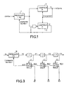
- FIG. 1 represents an example of a divider according to the prior art.
- the set works as follows: when the counter B arrives at the end of the count (which corresponds to the end of the frame), it delivers the signal TC which recharges the two counters respectively with the values A and B, respecting B ⁇ A. A new frame then begins. As long as the counter A has not finished counting, the matching stage 1 divides the input frequency Fe by Na + 1. That is, each time A and B are counted by one unit, the matching stage 1 counts (Na + 1) cycles of the input signal of period Te. The counter A arrives at the end of the count after A * (Na + 1) cycles of duration Te. At this moment, the counter A locks and controls the adaptation stage to divide by Na. To reach the end of counting, counter B must still count B-A, which corresponds to Na * (B-A) cycles of the input signal. The device then returned to the initial conditions.
- the retaining signal RX (K) is the command ⁇ NA.
- N0 is for example a power of 2
- the command NA varies for example from 2 P to 2 (P + 1) -1.
- precaler or adaptation stage means, in the present invention, a divider placed at the head of a division chain, generally having a simple structure and operating at high speed.
- Any other device having identical or substantially identical functional characteristics to this matching stage may be used.
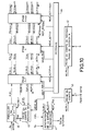
- FIG. 2 represents an exemplary embodiment of a frequency divider according to the invention.
- the matching stage has an input which receives the signal to be divided Fe, an input for a command NA of the division base of the adaptation stage, an input for a command NA / (NA + 1) ( to vary, the division rank of the matching stage of a unit, for example to increment one unit) from a block 11 comprising one or more identical or substantially identical division stages.
- the adaptation stage has, for example, a division rank NA varying from N0 to 2 * N0-1 where N0 is the minimum rank of the adaptation stage.
- NA can take the values 2 P to 2 (P + 1) -1 according to the value of the control word of the division rank NA, referenced 12 and represented by the bits R (1), R (2) .... R (P).
- an NA / NA + 1 command, referenced 13, which comes from the next division stage, divides by NA or NA + 1 according to the value 0 or 1 of this command.
- the value of P is chosen for example so that the adaptation stage has an optimal critical path).
- the adaptation stage is a divider by 1 which receives only the command NA / NA + 1 which makes it possible to divide by 1 or by 2.
- the command NA / NA + 1 makes it possible to carry out the variations 2 to 3 or 3 to 4 according to the value of R (1).
- the matching stage 10 is followed by Kmax-P stages which have identical or substantially identical functionality and which are put in series to form the divider.
- the divider thus formed in this exemplary embodiment makes it possible to divide by a rank of between 2 Kmax and 2 (Kmax + 1) -1 with a command RX (Kmax + 1) which makes it possible to increase the rank of division by one unit. .
- a division stage K comprises for example a divider by 2, referenced 14 K whose input is F (K-1) (frequency from the previous stage K-1) and whose output is F (K), frequency which corresponds to the entry of the next stage (K + 1).
- the stage K also comprises a two-input switch 15 K which is controlled by the output of the divider by 2, 14 K.
- a first input of the switch is the retaining signal RX (K + 1) which comes from the next stage (named (K + 1)), the second input of the switch is the programming data R (K), line 16 K .
- the output of the switch K is the retaining signal RX (K) which is one of the two inputs of the switch K-1 of the stage K-1.
- the output of the switch 15 P + 1 is the command NA / NA + 1 of the adaptation stage.
- the addition of the stage P + 1 behind the adaptation stage 10 makes it possible to obtain a divider which divides by a programmable rank NA 'between 2 (P + 1) to 2 (P + 2) -1 and which has an input RX (P + 2) which performs the command NA '/ NA' + 1.
- the addition of Kmax-P stages behind the adaptation stage makes it possible to obtain a divider which divides by a programmable rank between 2 (Kmax) and 2 (Kmax + 1) -1. This division rank can be incremented by 1 by the command RX (Kmax + 1).
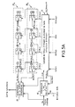
- FIG. 3 schematizes an example of a divider according to the invention comprising an adaptation stage 1/2, followed by 3 division stages by 2.
- the conventions used are the following: the divisors by 2 (14 1 , 14 2 , 14 3 ) change state on the rising edge of the input signal (F 0 , F 1 , F 2 ), the commands C 1 , C 2 , C 3 of the switches 15 1 , 15 2 , 15 3 , select the detentions RX2, RX3, RX4 coming from the next stage on the low states of the outputs F1, F2, F3 of the divisors by 2.
- stage K reads the reservoir from stage K + 1 on state of signal F ( K) which is located just before the F (K) front which triggers the state changes for the K + 1 stage.
- the counting frame duration of the divider is defined, for example, as being the period of time constituted by a high state and a low state of the output signal of the last stage (stage K 3 in this example, signal F3).
- This counting frame comprises 2 counting cycles of the stage K 2 . Each cycle consists of a high state and a low state whose durations can be different from one cycle to another depending on the propagation of the RX restraints.
- the counting frame thus contains 4 count cycles of the stage K 1 and 8 counting cycles of the adaptation stage 10.
- the counting frame contains 2 (Kmax-P) counting cycles of the adaptation stage when cascade Kmax-P division stages by 2 behind the adaptation stage. Each of these cycles has a duration that is NA or NA + 1 times the period of the input signal Fe.
- the duration of these 8 counting cycles is obtained by the propagation of the reservoirs during the counting frame (this propagation is carried out from downstream to upstream). This propagation is represented in Table 1 (FIG. 4) by lines RX3, RX2 and RX1. Having obtained the signal RX1, we successively deduce the durations of the different states of the signals F0, F1, F2 and F3 (the deduction is carried out from upstream to downstream).
- the duration of the counting frame is: (8 + 4R1 + 2R2 + R3 + RX4) * Te, where Te is the period of the input signal of the divider.
- Table 1 ( Figure 4) shows the propagation of the reservoirs and the duration of the high and low states for a 1/2 adaptation stage followed by 3 stages. Examination of the rows RX3, RX2 and RX1 of this table shows that: by going up the chain of switches, the reservoirs (for example R3) are progressively redrawn so that they are presented without additional impulses (in Anglo-Saxon terms). glitch) that can appear in relation to the logic levels provided for the head stage (here the adaptation stage).
- the chain of switches acts as a "funnel” for reservoirs that are progressively “resynchronized” to the adaptation stage. This "funnel” effect is used for refinements of the divider structure described hereinafter.
- the structure shown in FIG. 5A makes it possible to change the rank of division N statically (that is to say that there is a time of reconfiguration during which the output signal is not exploitable). This change is made by modifying the values R (K): one then obtains a rank N which can vary between 2 Kmax and 2 Kmax + 1 .
- R (K) the values of the funnel structure
- the start time of the frame is defined so as to locate the signals TC (P + 1) and MC (P + 1) with respect to this start of frame.
- the start of the frame designates the flank of the signal F (P) (input signal of the funnel structure) which triggers in cascade the transition to 1 of all divisors by 2 of the funnel structure, taking into account the conventions chosen.
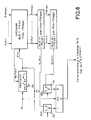
- the first type shown schematically in Figure 6, is a synchronous output that is the image of F (Kmax).
- the signals MC (P + 1) and TC (P + 1) which can for example be combined on a JK flip-flop, referenced 23, are used.
- the clock of the flip-flop JK is in general F (P) and Fe for a low rank adaptation stage.
- a second type of synchronous output is given in FIG. 7. It consists in particular in generating a constant state over the entire duration of the frame and in choosing with the aid of a command signal NEXT_POL (next polarity which makes it possible to choose a polarity of 0 or 1 of the synchronous output for the next frame - constant level on a frame).
- Two switches 24 1 and 24 2 each receive a signal TC (P + 1) and NEXT_POL and which are positioned just before the JK reference 23. In this type of output synchronous, only the signal TC (P + 1) is used.
- This variant embodiment can also use any other type of latches.
- a third type of synchronous output (not shown in the figures) consists in particular in sending the output TC (P + 1) on the inputs J and K so as to alternatively obtain a high state and a low state, each state having the given duration by N * Te where Te is the input period of the clock and N is the global division rank.
- the synchronous output shown in FIGS. 5A-8 is a resynchronization on F (P) which is the output of the adaptation stage or on Fe which is the input of the adaptation stage.
- F the output of the adaptation stage
- Fe the input of the adaptation stage.
- a resynchronization on the input Fe of the matching stage makes it possible to obtain increased performances of phase noise.
- the signals TC (P + 1), MC (P + 1) and RX (P + 1) are obtained without additional pulses. This is due to the principle of the funnel structure which works with inverse propagations: upstream to downstream for the chain of divisors by 2, downstream upstream for the chains RX, TC and MC.
- FIG. 8 shows an alternative embodiment making it possible to obtain on the synchronous output a divided signal of frequency Fe / N with N that can vary statically from 2 P to 2 (Kmax + 1) .
- the structure comprises two switches 25 and 26 which respectively receive the output of the matching stage F (P) and its complementary F P ⁇ .
- the block 22 comprises a flip-flop 23, for example of the JK type.
- the division rank N starts at the minimum rank of the adaptation stage.
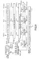
- FIG. 9 schematizes an example of a structure that makes it possible to change the rank of division from frame to frame, that is to say that while a frame is unfolding, the division device is given a new division rank for the next frame. This new frame will begin in perfect continuity from the end of the previous frame.
- It comprises an adaptation stage 10 dividing by NA varying from N0 to 2 * N0-1, for example from 2 P to 2 (P + 1) -1, followed by Kmax-P stages corresponding to the funnel structure (detailed structure in FIG. 2) as well as the switch chains delivering TC (P + 1) and MC (P + 1) according to the synchronous structure described in FIG. 5A.
- a first row 30 of registers are controlled by the intermediate outputs of the chain TC and a second row 31 of registers are controlled by the signal MC (P + 1).
- Figure 10 shows a block diagram of a multi-octave rank divider. Such a scheme makes it possible in particular to dynamically switch the rank of division over several octaves.
- Such a structure advantageously makes it possible to dynamically manage the counting length and thus to obtain a switchable division rank from frame to frame, of the value 2 (P + 1) (maximum division rank of the adaptation stage ) and 2 (Kmax + 1) (maximum division rank when all stages of the device are active).
- Figure 11 shows a schematic of a stage located behind the adaptation stage. The description is given by way of example for the stage of index K.
- the state machine delivers the DER (K) and ACT (K) signals.
- the DER signal (K) is used to manage the last stage quality for the K stage and is used by the functions developing the middle and end of count signals of stage K.
- the signal ACT (K) is an activation signal for the next stage.
- the activation signal controls the switch located at the output of the divider by 2. It is also transmitted to the next stage.
- stage K When the stage K is the last stage is the DER signal (K) which is cut by D (K) and transmitted on MC (K) during the 1 st part of the frame and TC (K) during the 2 th part of the frame.
- the asynchronous state machine comprises at least one storage latch ACT (K) which stores the active or inactive state of the next stage.
- ACT storage latch
- This embodiment variant including a simple asynchronous state machine in each stage of the divider makes it possible to obtain a division rank ranging from 2 P + 1 (maximum division rank of the adaptation stage) to 2 Kmax + 1 ( maximum division rank when all stages of the device are active).
- This divider still has an optimal consumption because all the management of the operation works at the speed of the stage concerned and it performs only a reduced number of operations per frame (and not per cycle which makes a big difference).
- this state machine consists of N flip-flops D which share the same clock input called CLK. A particular word of N bits stored in these flip-flops D represents a state of the machine. There are therefore 2 N possible states of the machine.
- the CLK input is connected to the output of a switch 2 N positions which is controlled by the state word of the machine, that is to say, by the N-bit bus consisting of all outputs Q of flip-flops D.
- the 2 N inputs of this switch are the 2 N clock signals that clock the sequence of states of the machine.
- Each D input of each flip-flop is also connected to the output of an input 2 N switch that is controlled by the N-output bus of the machine. Since there are N flip-flops there are N input switches which each have 2 N inputs, so there are in total N * 2 N data inputs for the machine.
Landscapes
- Stabilization Of Oscillater, Synchronisation, Frequency Synthesizers (AREA)
- Food-Manufacturing Devices (AREA)
Claims (11)
- Frequenzteiler, der das Teilen einer Frequenz Fe durch N erlaubt, der mindestens eine Anpassungsstufe (10) gefolgt von einer Teilungskette (11) aufweist, dadurch gekennzeichnet, dass:• die Anpassungsstufe (10) mindestens einen Eingang für das zu teilende Frequenzsignal Fe, einen Eingang für einen Befehl NA des Basisteilungsrangs der Anpassungsstufe und einen Eingang für einen Befehl ΔNA hat, der von der Teilungskette (11) kommt und es erlaubt, NA um eine Einheit variieren zu lassen,• die Teilungskette (11) mindestens eine Teilungsstufe (K) aufweist, die mindestens einen Teiler durch 2 aufweist, der eine geteilte Frequenz F(K) liefert, einen Umschalter (15K), der von dem Teiler durch 2 (14K) gesteuert wird, wobei der Umschalter (15K) einen Eingang für eine Programmierinformation R(K), einen Eingang für das Rückhaltesignal RX(K+1) der darauf folgenden Stufe und einen Ausgang für das Rückhaltesignal RX(K) für die vorhergehende Stufe hat.
- Frequenzteiler nach Anspruch 1, dadurch gekennzeichnet, dass der Befehl NA von N0 bis 2*N0-1 variiert.
- Frequenzteiler nach Anspruch 2, dadurch gekennzeichnet, dass der Befehl NA von 2P bis 2(P+1)-1 variiert.
- Frequenzteiler nach Anspruch 1, dadurch gekennzeichnet, dass er eine erste Kette von Umschaltern (20K) aufweist, die von den Ausgängen F(K) der Teiler (14K) gesteuert werden und ein Signal MC(P+1) liefern, eine zweite Kette von Umschaltern (21K), die von den Ausgängen F(K) der Teiler (14K) gesteuert werden und ein Signal TC(P+1) liefern, einen Block (22) zum Erzeugen eines synchronen Ausgangs, der ausgehend von den Signalen TC(P+1), MC(P+1) und dem Eingangssignal Fe oder F(P) des Ausgangs der Anpassungsstufe erstellt wird.
- Frequenzteiler nach Anspruch 4, dadurch gekennzeichnet, dass der Erzeugerblock (22) eine Kippschaltung des Typs JK (23) ist, die die Signale MC(P+1) und TC(P+1) sowie Fe oder F(P) empfängt.
- Frequenzteiler nach Anspruch 4, dadurch gekennzeichnet, dass er mindestens eine zweite Kette von Umschaltern (21K) aufweist, die von den Ausgängen F(K) der Teiler (14K) gesteuert werden und ein Signal TC(P+1) liefern, wobei mindestens zwei Umschalter (261) und (262) das Signal TC (P+1) empfangen und zwei Signale zu einer Kippschaltung (23) liefern, die das Eingangssignal oder das Ausgangssignal der Anpassungsstufe empfängt.
- Frequenzteiler nach Anspruch 4, dadurch gekennzeichnet, dass er eine erste Reihe von Registern (30) aufweist, die von den Zwischenausgängen der Kette (TC) gesteuert werden, und eine zweite Reihe von Registern (31), die von dem Signal MC(P+1) gesteuert werden.
- Frequenzteiler nach Anspruch 4, dadurch gekennzeichnet, dass er Folgendes aufweist:• eine Berücksichtigungsfunktion (42) in der Rahmenmitte des Teilungsrangs für den darauf folgenden Rahmen, wobei diese Funktion das Signal zum Schreiben MC(P+1) empfängt,• eine Funktion (43), die das Berücksichtungssignal des neuen Teilungsrangs NA der Anpassungsstufe erstellt,• eine Decodierfunktion (44), die es erlaubt, die Informationen NEXT_R (K), NEXT_ACT (K) und NEXT_NA ausgehend von dem Steuerwort N zu extrahieren.
- Frequenzteiler nach Anspruch 8, dadurch gekennzeichnet, dass er eine Berücksichtigungsfunktion (45) der Polung des synchronen Ausgangssignals für den nächsten Rahmen aufweist.
- Einsatz des Teilers gemäß einem der Ansprüche 1 bis 9 in dem Gebiet der Frequenzsynthese mit Phasenschleifen.
- Einsatz des Teilers gemäß einem der Ansprüche 1 bis 9 für einen Impulsgenerator.
Applications Claiming Priority (2)
| Application Number | Priority Date | Filing Date | Title |
|---|---|---|---|
| FR0301485A FR2851094B1 (fr) | 2003-02-07 | 2003-02-07 | Diviseur de frequence a structure entonnoir |
| FR0301485 | 2003-02-07 |
Publications (2)
| Publication Number | Publication Date |
|---|---|
| EP1445865A1 EP1445865A1 (de) | 2004-08-11 |
| EP1445865B1 true EP1445865B1 (de) | 2007-08-22 |
Family
ID=32606023
Family Applications (1)
| Application Number | Title | Priority Date | Filing Date |
|---|---|---|---|
| EP04100453A Expired - Lifetime EP1445865B1 (de) | 2003-02-07 | 2004-02-06 | Frequenzteiler mit Trichterstruktur |
Country Status (5)
| Country | Link |
|---|---|
| US (1) | US7002380B2 (de) |
| EP (1) | EP1445865B1 (de) |
| AT (1) | ATE371297T1 (de) |
| DE (1) | DE602004008357T2 (de) |
| FR (1) | FR2851094B1 (de) |
Families Citing this family (5)
| Publication number | Priority date | Publication date | Assignee | Title |
|---|---|---|---|---|
| JP4649859B2 (ja) * | 2004-03-25 | 2011-03-16 | ソニー株式会社 | 信号処理装置および方法、記録媒体、並びにプログラム |
| EP1675266B1 (de) * | 2004-08-27 | 2010-03-10 | STMicroelectronics Pvt. Ltd | Flächeneffizienter programmierbarer Frequenzteiler |
| FR2880219B1 (fr) * | 2004-12-23 | 2007-02-23 | Thales Sa | Procede et systeme de radiocommunication numerique, notamment pour les stations sol mobiles |
| DE102005013328B3 (de) * | 2005-03-22 | 2006-09-28 | Infineon Technologies Ag | Asynchroner Teiler mit einstellbarem Teilungsverhältnis |
| US20080315927A1 (en) * | 2007-06-11 | 2008-12-25 | Hynix Semiconductor Inc. | Frequency adjusting apparatus and dll circuit including the same |
Family Cites Families (7)
| Publication number | Priority date | Publication date | Assignee | Title |
|---|---|---|---|---|
| US4011516A (en) * | 1975-11-03 | 1977-03-08 | Rockwell International Corporation | Frequency correction arrangement |
| GB1560233A (en) * | 1977-02-02 | 1980-01-30 | Marconi Co Ltd | Frequency synthesisers |
| US4815018A (en) * | 1985-12-24 | 1989-03-21 | Hughes Aircraft Company | Spurless fractional divider direct digital frequency synthesizer and method |
| JP3468964B2 (ja) * | 1996-01-29 | 2003-11-25 | 富士通株式会社 | Pll周波数シンセサイザ回路、比較分周器、及び、スワロウカウンタ |
| US5867068A (en) * | 1997-10-27 | 1999-02-02 | Motorola, Inc. | Frequency synthesizer using double resolution fractional frequency division |
| US6035182A (en) * | 1998-01-20 | 2000-03-07 | Motorola, Inc. | Single counter dual modulus frequency division apparatus |
| DE19930168C2 (de) * | 1999-06-30 | 2001-07-19 | Infineon Technologies Ag | Schaltungsanordnung für einen Frequenzteiler |
-
2003
- 2003-02-07 FR FR0301485A patent/FR2851094B1/fr not_active Expired - Fee Related
-
2004
- 2004-02-06 US US10/772,584 patent/US7002380B2/en not_active Expired - Fee Related
- 2004-02-06 AT AT04100453T patent/ATE371297T1/de not_active IP Right Cessation
- 2004-02-06 DE DE602004008357T patent/DE602004008357T2/de not_active Expired - Lifetime
- 2004-02-06 EP EP04100453A patent/EP1445865B1/de not_active Expired - Lifetime
Also Published As
| Publication number | Publication date |
|---|---|
| DE602004008357D1 (de) | 2007-10-04 |
| ATE371297T1 (de) | 2007-09-15 |
| US7002380B2 (en) | 2006-02-21 |
| DE602004008357T2 (de) | 2008-05-15 |
| FR2851094B1 (fr) | 2005-04-15 |
| FR2851094A1 (fr) | 2004-08-13 |
| EP1445865A1 (de) | 2004-08-11 |
| US20040222825A1 (en) | 2004-11-11 |
Similar Documents
| Publication | Publication Date | Title |
|---|---|---|
| EP0645888B1 (de) | Digitale Verzögerungsleitung | |
| EP0171789B1 (de) | Rahmensynchronisiereinrichtung | |
| EP3242398B1 (de) | Generator von schwingungszahlen | |
| EP3375092B1 (de) | Verfahren zur synchronisation eines datenwandlers mithilfe eines im nahfeld übertragenen signales | |
| EP3242401B1 (de) | Schaltkreis zum zählen von impulsen | |
| FR3133458A1 (fr) | Circuit de génération de séquence temporelle | |
| EP1049285A1 (de) | Frequenzregelkreis | |
| EP0585996A1 (de) | Vorrichtung zum Umordnen der Bitrate von virtuellen Verbindungen bei asynchroner Zeitmultiplexübertragung | |
| FR2677515A1 (fr) | Circuit diviseur de frequence. | |
| EP0599746B1 (de) | Schnelle Zähler zum alternativen Auf- und Abzählen von Impulsfolgen | |
| EP0015014A1 (de) | Vorrichtung zur schnellen Synchronisierung eines Taktsignals | |
| EP0753941B1 (de) | Frequenzsynthetisierer | |
| EP1445865B1 (de) | Frequenzteiler mit Trichterstruktur | |
| FR2666707A1 (fr) | Dispositif de division de frequence programmable. | |
| EP0037299B1 (de) | Synchronisierungsanordnung für blockweise übertragene digitale Nachrichten | |
| FR3023396A1 (fr) | Generateur de nombres aleatoires | |
| EP3376670B1 (de) | Konfigurierbare verzögerungsleitung | |
| EP3242397B1 (de) | Multiplexerstruktur | |
| CA2040650C (fr) | Circuit de multiplexage de signaux d'horloge | |
| EP1557950A1 (de) | Frequenzteilungs-Verfahren und -Vorrichtung | |
| EP0536042B1 (de) | Verriegelungsdetektor eines digitalen Phasenregelkreises | |
| EP1606880B1 (de) | Frequenzteiler mit veränderlicher teilungsrate | |
| FR2962272A1 (fr) | Diviseur de frequence fractionnaire | |
| EP0707260B1 (de) | Asynchrone Speicheranordnung mit seriellem Zugriff und entsprechendes Speicher- und Leseverfahren | |
| FR2986679A1 (fr) | Generateur de nombres aleatoires vrais |
Legal Events
| Date | Code | Title | Description |
|---|---|---|---|
| PUAI | Public reference made under article 153(3) epc to a published international application that has entered the european phase |
Free format text: ORIGINAL CODE: 0009012 |
|
| AK | Designated contracting states |
Kind code of ref document: A1 Designated state(s): AT BE BG CH CY CZ DE DK EE ES FI FR GB GR HU IE IT LI LU MC NL PT RO SE SI SK TR |
|
| AX | Request for extension of the european patent |
Extension state: AL LT LV MK |
|
| 17P | Request for examination filed |
Effective date: 20050125 |
|
| AKX | Designation fees paid |
Designated state(s): AT BE BG CH CY CZ DE DK EE ES FI FR GB GR HU IE IT LI LU MC NL PT RO SE SI SK TR |
|
| GRAP | Despatch of communication of intention to grant a patent |
Free format text: ORIGINAL CODE: EPIDOSNIGR1 |
|
| GRAS | Grant fee paid |
Free format text: ORIGINAL CODE: EPIDOSNIGR3 |
|
| GRAA | (expected) grant |
Free format text: ORIGINAL CODE: 0009210 |
|
| AK | Designated contracting states |
Kind code of ref document: B1 Designated state(s): AT BE BG CH CY CZ DE DK EE ES FI FR GB GR HU IE IT LI LU MC NL PT RO SE SI SK TR |
|
| REG | Reference to a national code |
Ref country code: GB Ref legal event code: FG4D Free format text: NOT ENGLISH |
|
| REG | Reference to a national code |
Ref country code: CH Ref legal event code: EP |
|
| REG | Reference to a national code |
Ref country code: IE Ref legal event code: FG4D Free format text: LANGUAGE OF EP DOCUMENT: FRENCH |
|
| REF | Corresponds to: |
Ref document number: 602004008357 Country of ref document: DE Date of ref document: 20071004 Kind code of ref document: P |
|
| REG | Reference to a national code |
Ref country code: SE Ref legal event code: TRGR |
|
| GBT | Gb: translation of ep patent filed (gb section 77(6)(a)/1977) |
Effective date: 20071116 |
|
| PG25 | Lapsed in a contracting state [announced via postgrant information from national office to epo] |
Ref country code: FI Free format text: LAPSE BECAUSE OF FAILURE TO SUBMIT A TRANSLATION OF THE DESCRIPTION OR TO PAY THE FEE WITHIN THE PRESCRIBED TIME-LIMIT Effective date: 20070822 Ref country code: ES Free format text: LAPSE BECAUSE OF FAILURE TO SUBMIT A TRANSLATION OF THE DESCRIPTION OR TO PAY THE FEE WITHIN THE PRESCRIBED TIME-LIMIT Effective date: 20071203 Ref country code: BG Free format text: LAPSE BECAUSE OF FAILURE TO SUBMIT A TRANSLATION OF THE DESCRIPTION OR TO PAY THE FEE WITHIN THE PRESCRIBED TIME-LIMIT Effective date: 20071122 |
|
| PG25 | Lapsed in a contracting state [announced via postgrant information from national office to epo] |
Ref country code: AT Free format text: LAPSE BECAUSE OF FAILURE TO SUBMIT A TRANSLATION OF THE DESCRIPTION OR TO PAY THE FEE WITHIN THE PRESCRIBED TIME-LIMIT Effective date: 20070822 |
|
| REG | Reference to a national code |
Ref country code: IE Ref legal event code: FD4D |
|
| PG25 | Lapsed in a contracting state [announced via postgrant information from national office to epo] |
Ref country code: DK Free format text: LAPSE BECAUSE OF FAILURE TO SUBMIT A TRANSLATION OF THE DESCRIPTION OR TO PAY THE FEE WITHIN THE PRESCRIBED TIME-LIMIT Effective date: 20070822 Ref country code: GR Free format text: LAPSE BECAUSE OF FAILURE TO SUBMIT A TRANSLATION OF THE DESCRIPTION OR TO PAY THE FEE WITHIN THE PRESCRIBED TIME-LIMIT Effective date: 20071123 |
|
| PG25 | Lapsed in a contracting state [announced via postgrant information from national office to epo] |
Ref country code: CZ Free format text: LAPSE BECAUSE OF FAILURE TO SUBMIT A TRANSLATION OF THE DESCRIPTION OR TO PAY THE FEE WITHIN THE PRESCRIBED TIME-LIMIT Effective date: 20070822 Ref country code: PT Free format text: LAPSE BECAUSE OF FAILURE TO SUBMIT A TRANSLATION OF THE DESCRIPTION OR TO PAY THE FEE WITHIN THE PRESCRIBED TIME-LIMIT Effective date: 20080122 Ref country code: IE Free format text: LAPSE BECAUSE OF FAILURE TO SUBMIT A TRANSLATION OF THE DESCRIPTION OR TO PAY THE FEE WITHIN THE PRESCRIBED TIME-LIMIT Effective date: 20070822 Ref country code: SK Free format text: LAPSE BECAUSE OF FAILURE TO SUBMIT A TRANSLATION OF THE DESCRIPTION OR TO PAY THE FEE WITHIN THE PRESCRIBED TIME-LIMIT Effective date: 20070822 |
|
| PLBE | No opposition filed within time limit |
Free format text: ORIGINAL CODE: 0009261 |
|
| STAA | Information on the status of an ep patent application or granted ep patent |
Free format text: STATUS: NO OPPOSITION FILED WITHIN TIME LIMIT |
|
| PG25 | Lapsed in a contracting state [announced via postgrant information from national office to epo] |
Ref country code: RO Free format text: LAPSE BECAUSE OF FAILURE TO SUBMIT A TRANSLATION OF THE DESCRIPTION OR TO PAY THE FEE WITHIN THE PRESCRIBED TIME-LIMIT Effective date: 20070822 |
|
| 26N | No opposition filed |
Effective date: 20080526 |
|
| BERE | Be: lapsed |
Owner name: THALES Effective date: 20080228 |
|
| REG | Reference to a national code |
Ref country code: CH Ref legal event code: PL |
|
| PG25 | Lapsed in a contracting state [announced via postgrant information from national office to epo] |
Ref country code: CH Free format text: LAPSE BECAUSE OF NON-PAYMENT OF DUE FEES Effective date: 20080229 Ref country code: LI Free format text: LAPSE BECAUSE OF NON-PAYMENT OF DUE FEES Effective date: 20080229 Ref country code: MC Free format text: LAPSE BECAUSE OF NON-PAYMENT OF DUE FEES Effective date: 20080228 |
|
| PG25 | Lapsed in a contracting state [announced via postgrant information from national office to epo] |
Ref country code: EE Free format text: LAPSE BECAUSE OF FAILURE TO SUBMIT A TRANSLATION OF THE DESCRIPTION OR TO PAY THE FEE WITHIN THE PRESCRIBED TIME-LIMIT Effective date: 20070822 |
|
| PG25 | Lapsed in a contracting state [announced via postgrant information from national office to epo] |
Ref country code: BE Free format text: LAPSE BECAUSE OF NON-PAYMENT OF DUE FEES Effective date: 20080228 |
|
| PG25 | Lapsed in a contracting state [announced via postgrant information from national office to epo] |
Ref country code: SI Free format text: LAPSE BECAUSE OF FAILURE TO SUBMIT A TRANSLATION OF THE DESCRIPTION OR TO PAY THE FEE WITHIN THE PRESCRIBED TIME-LIMIT Effective date: 20070822 |
|
| PG25 | Lapsed in a contracting state [announced via postgrant information from national office to epo] |
Ref country code: CY Free format text: LAPSE BECAUSE OF FAILURE TO SUBMIT A TRANSLATION OF THE DESCRIPTION OR TO PAY THE FEE WITHIN THE PRESCRIBED TIME-LIMIT Effective date: 20070822 |
|
| PG25 | Lapsed in a contracting state [announced via postgrant information from national office to epo] |
Ref country code: LU Free format text: LAPSE BECAUSE OF NON-PAYMENT OF DUE FEES Effective date: 20080206 Ref country code: HU Free format text: LAPSE BECAUSE OF FAILURE TO SUBMIT A TRANSLATION OF THE DESCRIPTION OR TO PAY THE FEE WITHIN THE PRESCRIBED TIME-LIMIT Effective date: 20080223 |
|
| PG25 | Lapsed in a contracting state [announced via postgrant information from national office to epo] |
Ref country code: TR Free format text: LAPSE BECAUSE OF FAILURE TO SUBMIT A TRANSLATION OF THE DESCRIPTION OR TO PAY THE FEE WITHIN THE PRESCRIBED TIME-LIMIT Effective date: 20070822 |
|
| REG | Reference to a national code |
Ref country code: FR Ref legal event code: PLFP Year of fee payment: 13 |
|
| REG | Reference to a national code |
Ref country code: FR Ref legal event code: PLFP Year of fee payment: 14 |
|
| PGFP | Annual fee paid to national office [announced via postgrant information from national office to epo] |
Ref country code: SE Payment date: 20170213 Year of fee payment: 14 Ref country code: DE Payment date: 20170131 Year of fee payment: 14 Ref country code: FR Payment date: 20170126 Year of fee payment: 14 |
|
| PGFP | Annual fee paid to national office [announced via postgrant information from national office to epo] |
Ref country code: GB Payment date: 20170203 Year of fee payment: 14 Ref country code: NL Payment date: 20170210 Year of fee payment: 14 |
|
| PGFP | Annual fee paid to national office [announced via postgrant information from national office to epo] |
Ref country code: IT Payment date: 20170221 Year of fee payment: 14 |
|
| REG | Reference to a national code |
Ref country code: DE Ref legal event code: R119 Ref document number: 602004008357 Country of ref document: DE |
|
| REG | Reference to a national code |
Ref country code: SE Ref legal event code: EUG |
|
| REG | Reference to a national code |
Ref country code: NL Ref legal event code: MM Effective date: 20180301 |
|
| GBPC | Gb: european patent ceased through non-payment of renewal fee |
Effective date: 20180206 |
|
| PG25 | Lapsed in a contracting state [announced via postgrant information from national office to epo] |
Ref country code: SE Free format text: LAPSE BECAUSE OF NON-PAYMENT OF DUE FEES Effective date: 20180207 |
|
| REG | Reference to a national code |
Ref country code: FR Ref legal event code: ST Effective date: 20181031 |
|
| PG25 | Lapsed in a contracting state [announced via postgrant information from national office to epo] |
Ref country code: NL Free format text: LAPSE BECAUSE OF NON-PAYMENT OF DUE FEES Effective date: 20180301 |
|
| PG25 | Lapsed in a contracting state [announced via postgrant information from national office to epo] |
Ref country code: DE Free format text: LAPSE BECAUSE OF NON-PAYMENT OF DUE FEES Effective date: 20180901 |
|
| PG25 | Lapsed in a contracting state [announced via postgrant information from national office to epo] |
Ref country code: FR Free format text: LAPSE BECAUSE OF NON-PAYMENT OF DUE FEES Effective date: 20180228 Ref country code: IT Free format text: LAPSE BECAUSE OF NON-PAYMENT OF DUE FEES Effective date: 20180206 Ref country code: GB Free format text: LAPSE BECAUSE OF NON-PAYMENT OF DUE FEES Effective date: 20180206 |