EP3242397B1 - Multiplexerstruktur - Google Patents
Multiplexerstruktur Download PDFInfo
- Publication number
- EP3242397B1 EP3242397B1 EP16198958.7A EP16198958A EP3242397B1 EP 3242397 B1 EP3242397 B1 EP 3242397B1 EP 16198958 A EP16198958 A EP 16198958A EP 3242397 B1 EP3242397 B1 EP 3242397B1
- Authority
- EP
- European Patent Office
- Prior art keywords
- output
- multiplexer
- delay
- generator
- signal
- Prior art date
- Legal status (The legal status is an assumption and is not a legal conclusion. Google has not performed a legal analysis and makes no representation as to the accuracy of the status listed.)
- Active
Links
Images


Classifications
-
- G—PHYSICS
- G06—COMPUTING OR CALCULATING; COUNTING
- G06F—ELECTRIC DIGITAL DATA PROCESSING
- G06F21/00—Security arrangements for protecting computers, components thereof, programs or data against unauthorised activity
- G06F21/70—Protecting specific internal or peripheral components, in which the protection of a component leads to protection of the entire computer
- G06F21/71—Protecting specific internal or peripheral components, in which the protection of a component leads to protection of the entire computer to assure secure computing or processing of information
- G06F21/73—Protecting specific internal or peripheral components, in which the protection of a component leads to protection of the entire computer to assure secure computing or processing of information by creating or determining hardware identification, e.g. serial numbers
-
- H—ELECTRICITY
- H03—ELECTRONIC CIRCUITRY
- H03K—PULSE TECHNIQUE
- H03K17/00—Electronic switching or gating, i.e. not by contact-making and –breaking
- H03K17/002—Switching arrangements with several input- or output terminals
- H03K17/005—Switching arrangements with several input- or output terminals with several inputs only
-
- G—PHYSICS
- G06—COMPUTING OR CALCULATING; COUNTING
- G06F—ELECTRIC DIGITAL DATA PROCESSING
- G06F7/00—Methods or arrangements for processing data by operating upon the order or content of the data handled
- G06F7/58—Random or pseudo-random number generators
-
- G—PHYSICS
- G06—COMPUTING OR CALCULATING; COUNTING
- G06F—ELECTRIC DIGITAL DATA PROCESSING
- G06F7/00—Methods or arrangements for processing data by operating upon the order or content of the data handled
- G06F7/58—Random or pseudo-random number generators
- G06F7/588—Random number generators, i.e. based on natural stochastic processes
-
- H—ELECTRICITY
- H03—ELECTRONIC CIRCUITRY
- H03K—PULSE TECHNIQUE
- H03K19/00—Logic circuits, i.e. having at least two inputs acting on one output; Inverting circuits
- H03K19/003—Modifications for increasing the reliability for protection
-
- H—ELECTRICITY
- H03—ELECTRONIC CIRCUITRY
- H03K—PULSE TECHNIQUE
- H03K19/00—Logic circuits, i.e. having at least two inputs acting on one output; Inverting circuits
- H03K19/02—Logic circuits, i.e. having at least two inputs acting on one output; Inverting circuits using specified components
- H03K19/173—Logic circuits, i.e. having at least two inputs acting on one output; Inverting circuits using specified components using elementary logic circuits as components
- H03K19/1733—Controllable logic circuits
- H03K19/1737—Controllable logic circuits using multiplexers
-
- H—ELECTRICITY
- H03—ELECTRONIC CIRCUITRY
- H03K—PULSE TECHNIQUE
- H03K3/00—Circuits for generating electric pulses; Monostable, bistable or multistable circuits
- H03K3/84—Generating pulses having a predetermined statistical distribution of a parameter, e.g. random pulse generators
-
- H—ELECTRICITY
- H03—ELECTRONIC CIRCUITRY
- H03K—PULSE TECHNIQUE
- H03K5/00—Manipulating of pulses not covered by one of the other main groups of this subclass
- H03K5/159—Applications of delay lines not covered by the preceding subgroups
Definitions
- the present description relates generally to electronic circuits and, more particularly, to electronic circuits or functions usable as in an electronic circuit or device.
- An example of application of the electronic circuits and functions of the present description is the realization of a random number generator.
- Another example of application is the realization of a physical unclonable function (PUF), for example to generate unique identifiers or unique cryptographic keys.
- PEF physical unclonable function
- the present description relates more particularly to random number generators in security applications such as encryption, authentication, etc.
- processing units such as central processing units (CPUs) in microcontrollers, use randomly generated numbers.
- Random number generation circuits use various circuits or subassemblies that may have other applications outside of random number generation.
- a random number generator uses oscillator, multiplexer, etc. type circuits which, although particularly interesting in the generation of random numbers, are not limited to these applications.
- the number generators to which this description applies are based on the use of delay lines looped back to each other.
- One embodiment overcomes all or part of the drawbacks of the usual solutions for generating random numbers or physical functions for unique identifiers, cryptographic keys, etc.
- An embodiment according to one aspect of the present disclosure provides a circuit whose behavior is modelable to realize an oscillation number generator for the purpose of generating random numbers or an unclonable number.
- An embodiment according to this aspect provides a generator whose behavior can be verified.
- An embodiment according to this aspect provides a solution compatible with the use of standard cells of a given electronic technology.
- An embodiment according to another aspect of the present description proposes a symmetrical multiplexer structure, that is to say having a similar temporal behavior for transiting a rising edge and for transiting a falling edge.
- An embodiment according to this further aspect provides a multiplexer structure compatible with conventional multiplexer structures.
- An embodiment according to yet another aspect of the present description provides a counter for changing the state (oscillations) of noisy signals.
- An embodiment according to this yet further aspect proposes a solution more particularly suited to counting an output of an oscillation generator.
- an embodiment of a first aspect not forming part of the invention provides a circuit for generating a number of oscillations.
- one half of said multiplexers has its control inputs connected to said control terminal.
- the other half of the multiplexers have their control inputs connected to the output of an inverter, one input of which is connected to said control terminal.
- One embodiment also provides a four-to-one multiplexer, comprising three two-to-one logic multiplexers.
- One embodiment also provides a number generation circuit, comprising at least one multiplexer as above.
- An embodiment of a third aspect not forming part of the invention provides a circuit for counting pulses provided by a circuit having at least two terminals for providing inverted pulse signals.
- the number generator that is the subject of the present description is described below in relation to an example of a random number generator of oscillations. Unless otherwise specified, everything that is described below applies, however, to an oscillation number generator for a non-clonable physical function.
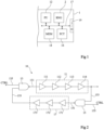
- FIG 1 represents, very schematically, an electronic circuit 1 of the type to which the embodiments which will be described apply.
- FIG. 2 represents an example of an electrical diagram of a usual generator 10 of a number of oscillations for a random number generator.
- This generator 10 is based on two delay lines each composed of delay elements in series, looped back to each other, each delay element restoring the signal in the same state (1 or 0) as its input.
- the number of delay elements in each chain may be different or identical.
- a first line 11 comprises four delay elements 111, 112, 113 and 114 in series between an output terminal 131 of a first NAND type logic gate 13 and a first input terminal 153 of a second NAND type logic gate 15.
- a second line 17 comprises three delay elements 171, 172 and 173 in series between an output terminal 151 of the second gate 15 and a first input 133 of the first gate 13.
- the respective second inputs 135 and 155 of the logic gates 13 and 15 constitute input terminals intended to receive the same CTRL control signal (triggering the generation of a number).
- the number of oscillations which conditions the random number, is taken, for example, at the output of the first line, that is to say on the first input 153 of the gate 15. Alternatively, the number of oscillations is taken at the input 133 of the gate 13, at the output 131 of the gate 13 or at the output 151 of the gate 15.
- the difference between the delays introduced by the two lines determines the duty cycle of the signals present at terminals 133 and 153.
- the generator of the figure 2 oscillates indefinitely with a duty cycle as long as the CTRL signal is at state 1.
- the generator in the absence of noise but with delay elements (logic gates) having different times which eventually distort the duty cycle enough for the oscillator to stop, the generator eventually stops after a fixed number of oscillations.
- the generator In the presence of noise (phase jitter), the generator eventually stops but after a number of oscillations whose value varies.
- the inventors found that it was possible to link the behavior of the oscillation number generator to the intrinsic but quantifiable parameters of the elements that constitute it.
- FIGS. 3A, 3B, 3C, 3D and 3E illustrate, by means of timing diagrams, the theoretical operation of the circuit of the figure 2 .
- FIG 3A represents an example of the appearance of the CTRL signal.
- the Figure 3B illustrates a corresponding example of the shape of the signal present at output 131 of gate 13.
- the Figure 3C illustrates a corresponding example of the shape of the signal present on the output of the first line (input 133 of gate 13).
- the 3D figure illustrates a corresponding example of the shape of the signal present at output 151 of gate 15.
- the Figure 3E illustrates a corresponding example of the shape of the signal present on the output of the first line (input 153 of gate 15).
- the CTRL signal is switched to state 1 to activate the generation.
- the outputs 131 and 151 switch to state 0 at a time t31.
- Lines 11 and 13 provide delays of 4*td u and 3*td u respectively to the rising and falling edges of the signals present at terminals 131 and 151. Consequently, the signal 133 switches to state 0 at a time t32, 3*td u later than the time t31, and the signal 153 switches to state 0 at a time t33, 4*td u later than the time t31.
- Signals 131 and 151 then switch to state 0 with a delay td u relative to times t32 and t33 respectively, and so on.
- the number of oscillations taken, preferably at output 153 (or 133), when the oscillation stops, is random. Note that this number of oscillations can be counted at any point in the loop.
- the inventors consider that, in addition to phase noise, one of the factors that leads to the generator stopping comes in particular from an imbalance between the rise times and the fall times of the signals, that is to say between the time taken by a delay element or a gate to switch from state 1 to state 0 and from state 0 to state 1.
- the difference between the rise times and fall times of a branch of the generator means that there comes a time when the duration of a state becomes less than the delay provided by an element of the delay line.
- the behavior of the generator can be written from arithmetic sequences.
- L1 n + 1 L1 n + ⁇ fr1 ⁇ ⁇ fr 2 .
- H 2 n H 2 0 ⁇ n * r .
- the ratio r the difference between the rise times and the fall times (the ratio r) is negative, the L1 and H2 durations increase while the L2 and H1 durations decrease. Conversely, if the ratio r is positive, the L2 and H1 durations decrease while the L1 and H2 durations increase.
- each branch is composed of a delay line 21, respectively 27, called symmetrical, that is to say having identical or very close rise and fall times (difference between the rise and fall time less than one tenth of the ratio r) in series with an element 22, respectively 24, called asymmetrical, whose rise and fall times are different from each other.
- An input terminal 231 of the first branch is connected to the output of a first logic gate 23 of the NAND type, a first input 235 of which receives a trigger signal CTRL and a second input 233 of which receives the output of the second branch.
- An output terminal 253 of the first branch is connected to a first input of a second gate 25 of the NAND type, a first input 255 of which receives the CTRL signal and the output 251 of which is connected to the input of the second branch.
- the output of the generator of a random number of oscillations is for example terminal 253 or terminal 233.
- this output therefore the counting of oscillations, can correspond alternatively to output 231 or 251 of gate 23, respectively 25, or more generally to any point of the loop.
- the output is connected to the output of an asynchronous counter of the number of oscillations which counts the number of oscillations between activation of the generator by the CTRL signal and stopping of the oscillations.
- This counter (not shown in figure 4 ) is, for example, made up of one or more flip-flops in cascade, the clock input of the first flip-flop receiving the output signal of the generator.
- the output(s) of the flip-flops provide a number on one or more bits (depending on the number of flip-flops) of which generally only the bits or the least significant bit are kept to constitute the random number.
- multiple generators are used in parallel to increase the rate of generated random bits.
- paired inverters are preferably used, that is to say an even number of inverters in each line.
- line 21 has p pairs of inverters 3 in series while line 27 has q pairs of inverters 3 in series.
- the numbers p and q may be the same or different from each other.
- any inverter design can be used (e.g. CMOS inverters made of two transistors in series, NOR or NAND gates with inputs interconnected, etc.) provided that these inverters respect the condition of associating, when they are paired in series, successively rise time and fall time, or vice versa, so that these times are summed regardless of the edge present at the input.
- CMOS inverters made of two transistors in series, NOR or NAND gates with inputs interconnected, etc.
- a non-inverting logic amplifier (buffer) type element is used, excluding two identical inverters in series.
- an OR gate an AND gate whose two inputs are connected, or any logic function that can be reduced to an inverting function depending on only one input and whose rise and fall times are different, can be used.
- Each element 22 and 24 is chosen to have a rise time different from its fall time.
- elements 22 and 24 are chosen to have different differences between rise times and fall times. Thus, the differences that will determine the stopping of the generator are introduced.
- gates 23 and 25 also provide a shift between the rise and fall times of each branch. This shift must be added to that introduced by element 24, respectively 22, to obtain the deviations, respectively ⁇ fr 1 and ⁇ fr 2 , therefore the reasons for the arithmetic sequences.
- a single element 22 or 24 is provided, the other branch having only the symmetrical delay line.
- Lines 21 and 27 may be placed either upstream or downstream of elements 22 and 24 with which they are respectively associated.
- elements 22 and 24 are even intercalated inside lines 21 and 27, between inverters or pairs of inverters which constitute them.
- An advantage of the embodiments described is that it is now easy to size an oscillation generator and to be able to characterize it. Thus, when designing an electronic circuit comprising a random number generator, knowing the differences between the rise and fall times in the technology, it becomes easy to comply with specifications.
- the interpretation of the generated number is done by counting the pulses on one of the outputs 233 and 253 and taking, as a random bit, for example, the least significant bit at the end of the counting period.
- the counting period is set by a clock signal.
- FIG. 5 schematically represents an alternative embodiment according to which we seek to minimize the reason for the arithmetic sequence, while keeping it easily determinable.
- a second symmetrical delay line (SDL) 26, respectively 28, is provided in parallel with each element 22, 24 or asymmetrical delay line (ADL - Asymmétrie Delay Line).
- the inputs of the delay lines 22 and 26 are connected to the output of the line 21.
- the inputs of the lines 24 and 28 are connected to the output of the line 27.
- the outputs of the lines 22 and 26, respectively 24 and 28, are connected to inputs of a two-to-one multiplexer 51, respectively 52, the output of which is connected to input 253, respectively 233, of the logic gate 25, respectively 23.
- the multiplexer 51 is controlled by a signal resulting from a count (counter 53, CNTH) of the pulses of its output signal.
- the counter determines the number of pulses from which one switches from the asymmetrical line 22 to the symmetrical line 26.
- control can be provided by the same counter 53 or by a different counter which then counts the pulses from the output of the multiplexer 52. In practice, if a single counter is used, it is placed on the branch with the longest delay so as not to switch the multiplexers before the end of the first pulses.
- Such a variant makes it possible to make the reason of arithmetic sequences configurable and more particularly to reduce this reason in order to delay the stopping of the generator.
- the reason r is divided by the number of loops. This allows, among other things, to increase the number of pulses circulating in the delay lines of the generator while reducing the size of these delay lines.
- counter 53 is the pulse counting counter whose least significant bit(s) are used, when the oscillations stop, to define the random number generated.
- FIG. 6 represents an embodiment of a delay line 6, configurable both in symmetrical delay and in asymmetrical delay.
- the realization of the figure 6 may constitute, as a particular example in the preceding embodiments, an embodiment of the symmetrical delay line, for example 21, and of the asymmetrical delay element, for example 22, of a branch.
- one or more (in the example three) symmetrical delay lines 212, 214 and 216 are associated with one or more (in the example three) delay elements or asymmetrical delay lines 221, 223, 225, that is to say each having different rise and fall times, each asymmetrical or symmetrical line being short-circuitable using a multiplexer 61, 62, 63, 64, 65, 66 respectively.
- the inputs of lines 212, 214, 216, 221, 223 and 225 are respectively directly connected to a first input of multiplexers 61, 62, 63, 64, 65, 66 whose other input is connected to the output of the corresponding delay line.
- the outputs of multiplexers 61, 62, 63, 64 and 65 are respectively connected to the inputs of lines 214, 216, 221, 223, 225 and the output of multiplexer 66 defines the output OUT of the parameterizable delay line.
- Each multiplexer 61 to 66 is individually controllable, for example, by a different bit, respectively [5], [4], [3], [2], [1], [0] of a SEL_DLY word.
- the input terminal IN of line 6 is connected to the output (231 or 251, figures 4 And 5 ) of the branch concerned.
- Each line 212, 214, 216 is preferably made up of one or more pairs of inverters, i.e. delay elements each having identical rise and fall times as described above.
- lines 212, 214 and 216 respectively comprise 32, 16 and 8 pairs of inverters, i.e. 32, 16 and 8 unitary symmetrical delay elements (sdelt).
- the asymmetric lines 221, 223, 225 provide delays that are identical or different from each other.
- the lines 221, 223 and 225 are made up of identical unit elements, i.e. providing the same offset between rise time and fall time. Different numbers of these unit elements are then provided in each of the lines, which makes the system easily configurable with optimal granularity.
- the lines 221, 223 and 225 respectively comprise 4, 2 and 1 unit asymmetric delay elements (adelt).
- the delay line 6 is configurable both in delay and in difference between rise time and fall time. Taking the example of identical unit elements in lines 212, 214 and 216, and of identical unit elements in lines 221, 223 and 225, it is possible to choose a symmetrical delay between 8 and 56 times the delay of the symmetrical unit element and a time difference between rising edge and falling edge between 1 and 7 times the difference provided by the asymmetrical unit element.
- the unit elements are, for example, made as described above in relation to the figure 4 .
- the number of symmetrical and asymmetrical delay lines depends on the desired tuning capability.
- Asymmetrical elements not only have different rise and fall times but also an intrinsic delay that contributes to the total delay of the delay line.
- the realization of the figure 6 can be used, for example, to integrate the same generator architecture and to make this structure configurable, whether at the design stage or in the application.
- the realization of the figure 6 can be combined with that of the figure 5 by placing in parallel with each asymmetrical line 221, 223, 225, a symmetrical line of the same delay, thus eliminating the short circuit of the line attacking the upper inputs (in the orientation of the figure 6 ) multiplexers 64 to 66.
- 3 to 1 multiplexers are used, two of whose inputs receive the respective outputs of two parallel lines of the same delay, respectively symmetrical and asymmetrical, and the third input of which directly receives the output of the multiplexer of the previous rank.
- the multiplexers 61 to 66 In the realization of the figure 6 or its variants, in order to facilitate the parameterization, it would be desirable for the multiplexers 61 to 66 to provide symmetrical delays. However, a usual multiplexer has an asymmetrical operation in terms of rise time and fall time.
- FIG. 7 represents an embodiment according to the invention of a multiplexer 7 having symmetrical operation, that is to say an identical rise time and fall time.
- Multiplexer 7 of the figure 7 is a two-to-one multiplexer, that is, it selects one of its two inputs A or B and provides the corresponding signal at output Z. The selection between input A or B is made by a control signal S.
- the multiplexer 7 comprises four two-to-one multiplexing or selection elements.
- the multiplexer 7 can be considered to consist of 4 unit multiplexers 72, 74, 76 and 78 associated in a chain.
- the multiplexers are inverting multiplexers.
- a first multiplexer 72 has its input terminals respectively connected to inputs A and B.
- a second multiplexer 74 has its two inputs connected together to the output of the first multiplexer 72.
- a third multiplexer 76 has its two inputs connected together to the output of the second multiplexer 74.
- a fourth multiplexer 78 has its two inputs connected together to the output of the third multiplexer 76 and its output provides the output Z.
- the signal S directly controls the multiplexers 72 and 74 and, after passing through an inverter 75, the multiplexers 76 and 78.
- multiplexers 74, 76, and 78 have their inputs interconnected means that they do not actually perform any selection. However, assuming that all multiplexers 72, 74, 76, and 78 are identical, they all have identical rise and fall times. Furthermore, they all have similar behavior on an edge on their first input and all have similar behavior on an edge on their second input.
- tr AZ tr HAS 72 + tr HAS 74 + tr B 76 + tr B 78 ;
- tf AZ tr HAS 72 + tf HAS 74 + tr B 76 + tf B 78 ;
- tr BZ tf B 72 + tr B 74 + tf HAS 76 + tr HAS 78 ;
- tf BZ tr B72 + tf B74 + tr A76 + tf A78 .
- the rise and fall times of the multiplexer 7 are identical regardless of the input considered.
- the multiplexer is therefore symmetrical with the definition given above.
- An advantage of the embodiment of the figure 7 is that it ensures that the selection of multiplexers 76 and 78 is active before the signal (the edge) has finished passing through multiplexers 72 and 74.
- An advantage of the embodiment of the figure 7 is that it is independent of the internal structure of the unit multiplexers. Indeed, provided that identical unit multiplexers are used, the operation described is respected.
- a multiplexer as shown in figure 7 has multiple applications. In particular, it is often advantageous to have symmetrical operation.
- the multiplexer of the figure 7 can be used to realize each of the multiplexers 61, 62, 63, 64, 65 and 66 of the realization of the figure 6 .
- An advantage is then that the reason for the pulse sequences of the number generator remains only linked to the asymmetric elements 221, 223 and 225, which facilitates dimensioning.
- the structure of the multiplexer 7 of the figure 7 can be adapted to create multiplexers with more than two inputs.
- FIG 8 represents an embodiment of a symmetrical 8 four-to-one multiplexer.
- a first multiplexer 7a defines two inputs A and B.
- a second multiplexer 7b defines inputs C and D.
- the respective outputs of the multiplexers 7a and 7b are connected to the two inputs of a third multiplexer 7c whose output defines the output Z' of the four-to-one multiplexer.
- the multiplexers 7a and 7b are respectively controlled by a signal S1 and by its inverse.
- the multiplexer 7c is controlled by a signal S2. For example, assuming a two-bit selection word, the signal S2 is made up of the most significant bit and the signal S1 is made up of the least significant bit.
- the interpretation of the generator output requires counting the pulses present at the output. It is this counting that determines the number drawn. For example, the least significant bit of the count of the pulses present at the generator output between its triggering and a reading signal from the counter, subsequent to the stopping of the oscillations, is taken as the random bit generated by the generator 20.
- the time interval between the triggering of the generator and the reading signal is chosen according to the range of possible time intervals conditioned by the dimensioning of the generator delay lines.
- This problem is likely to arise not only in counting the number of oscillations in a generator as described in the present description but more generally to count short duration events in a signal, for example a glitch detector.
- a counter whether asynchronous or not, normally operates with a clock, called square, i.e. with a duty cycle close to 50%.
- the duty cycle of the asynchronous counter clock which corresponds to output 231 or 251 (or 233, 253), decreases at each period until the oscillation stops, or on the contrary increases at each period until the oscillation stops. Consequently, one of the outputs stops at state 0 and the other stops at state 1.
- flip-flops are used that require in their specifications a minimum duration of the clock in the high state (1) and a minimum duration of the clock signal in the low state (0), for example arbitrarily 110 ps for the minimum duration in the high state and 87 ps for the minimum duration in the low state. Therefore, when the input flip-flop of the counter receives a clock with a very low or very high duty cycle, it can end up operating out of specification and the clock signal pulse is then not taken into account.
- FIG 9 represents an embodiment of a random number generator of the type described above with its pulse counting elements for shaping the generated number.
- each output 251, 231 of the random oscillation number generator 20 is connected to the input of a counter, respectively 91 (CNTR), 93 (CNTL).
- Each counter 91, 93 counts the pulses of the corresponding output signal of the generator.
- Each counter is an asynchronous counter, for example of the D flip-flop type.
- circuit 95 receives output signals 231 and 251 in order to know, during the decision, the states of these signals at the end of the oscillations.
- oscillation count counters one with one output of generator 20, the other with the other output of generator 20.
- one of the counters will stop operating before the other, that is, its input flip-flop will stop operating before the input flip-flop of the other, due to the fact that the minimum operating times of the flip-flops are different for the low state and for the high state.
- one of the counters will stop under the effect of an oscillation not respecting its minimum time in the low state while the other counter will stop under the effect of an oscillation not respecting its minimum time in the high state.
- the selection criterion by circuit 95 between the outputs of counters 91 and 93 according to the states provided by outputs 231 and 251, differs.
- This selection criterion can be conditioned by a simulation of the operation of the generator in order to determine whether the flip-flops stop because of the minimum time in the high state or because of the minimum time in the low state.
- the counter that stops last is selected.
- block 95 selects the result of the counter that stops first, that is to say the first one that, during a change of state of output 231 or 251, does not change its least significant bit.
- This exemplary embodiment is preferred in the case where the cause of stopping of the flip-flops (minimum time in the low state or minimum time in the high state) has not been determined in simulation.
- the counting circuit described in relation to the figure 9 applies more generally to any random number generator and not necessarily to that of the figure 4 .
- it can be implemented for any random number generator having delay lines looped back to each other (for example, figure 2 ).
- the signals provided by the outputs 253 and 233 are shaped before being counted in order to eliminate certain possible failures in the counting.
- optional shaping circuits (SHAPER) 97 are interposed between the respective outputs 251 and 231 and the counters 91 and 93.
- FIG 10 represents an embodiment of a circuit 97 for shaping a pulse signal.
- Circuit 97 includes a D-type flip-flop 972 whose input D is forced to the high state (1) and whose non-inverted output Q defines the output S97 providing the shaped signal.
- the clock input CK of flip-flop 972 defines the input of the circuit receiving the pulse signal to be shaped.
- the inverted output NQ of flip-flop 972 is connected, via a non-inverting delay element 974 (DELAY), to a first input of an AND-type logic gate 976, one output of which is connected to the reset input RN (active on rising edge) of flip-flop 972.
- a second input of gate 976 is intended to receive an RSTN signal for activating circuit 97. When signal RSTN is at state 0, circuit 97 is not active and output S97 is permanently at state 0. Gate 976 is therefore optional if there is no need to deactivate circuit 97.
- the value of the delay introduced by element 974 is chosen to be greater than the minimum pulse width that the D flip-flop can capture.
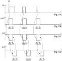
- FIGS. 11A, 11B, 11C and 11D illustrate, in the form of timing diagrams, the operation of the shaping circuit of the figure 10 .
- FIG 11A represents an example of the shape of the input signal CK to be shaped.
- the Figure 11B shows an example of the corresponding shape of the signal of the Q output (S97).
- the Figure 11C represents an example of a corresponding appearance of the NQ output.
- the Figure 11D represents an example of the corresponding shape of the RN input signal.
- the Q output (therefore the S97 output) is at state 0
- the NQ output is at state 1.
- the RN input is at state 1.
- the RSTN signal is active (state 1).
- the right part of the timing diagrams illustrates the operation with a CK pulse of duration less than the DELAY delay.
- the DELAY delay sets the duration of the output signal pulses independently of the duration of the CK signal pulse. Therefore, even though the CK signal pulse is theoretically too short for its fall to be taken into account, it is still present on the Q output.
- the DELAY duration sets the duration of the pulses of the S97 signal, therefore of the input of the counters in the realization of the figure 10 .
- the output of gate 976 is connected to the set input of the flip-flop, the input is forced to state 0 and the delay element receives the non-inverted output Q while the output of the shaping circuit is defined by the inverted output NQ.
- An advantage of the embodiments that have been described is that they allow a random number generator to be designed or configured in a reliable and determinable manner. Thus, it is possible to meet the criteria set by a specification and validate that the generator meets these specifications.
- Another advantage is that the described solution is compatible with the use of standard cells of a given technology.
- Another advantage is that the entire generator is realizable with logic elements.
- the number is taken either after a fixed time interval, triggered by the activation of the generator (CTRL signal) and chosen to be greater than the maximum stop time of the generator), or by detecting the stopping of the counter(s).
- the delay lines and the reason of the arithmetic sequences are sized in order to fix the number of oscillations.
- the number is sampled after stopping the generator as for a random number generator and preferably only a part of the bits (the most significant) are kept.
Landscapes
- Physics & Mathematics (AREA)
- Engineering & Computer Science (AREA)
- General Engineering & Computer Science (AREA)
- Theoretical Computer Science (AREA)
- General Physics & Mathematics (AREA)
- Computer Hardware Design (AREA)
- Mathematical Physics (AREA)
- Computing Systems (AREA)
- Pure & Applied Mathematics (AREA)
- Mathematical Optimization (AREA)
- Mathematical Analysis (AREA)
- Computational Mathematics (AREA)
- Nonlinear Science (AREA)
- Computer Security & Cryptography (AREA)
- Software Systems (AREA)
- Pulse Circuits (AREA)
- Electronic Switches (AREA)
- Stabilization Of Oscillater, Synchronisation, Frequency Synthesizers (AREA)
Claims (5)
- Logischer Zwei-zu-Eins-Multiplexer (7), der Folgendes aufweist:zwei Eingangsanschlüsse (A, B);einen Ausgangsanschluss (Z);einen Steueranschluss (S); undein Vielfaches von vier Zwei-zu-Eins-Einheitsmultiplexern (72, 74, 76, 78), die alle invertierend und identisch sowie in Reihe geschaltet sind, wobei das Vielfache von vier Multiplexern Folgendes aufweist:einen ersten Einheitsmultiplexer (72), dessen Eingänge mit den Eingangsklemmen verbunden sind;einen letzten Einheitsmultiplexer (78), dessen Ausgang mit dem Ausgangsanschluss verbunden ist, und wobeider letzte und die anderen Einheitsmultiplexer (74, 76) des Vielfachen ihre jeweiligen Eingänge direkt mit dem Ausgang des vorherigen Multiplexers in der Reihenschaltung verbunden haben, unddie Hälfte der Einheitsmultiplexer des Vielfachen in Bezug auf die andere Hälfte umgekehrt (75) gesteuert wird.
- Multiplexer nach Anspruch 1, wobei die Steuereingänge der Hälfte der Multiplexer mit dem Steueranschluss (S) verbunden sind.
- Multiplexer nach Anspruch 2, wobei die Steuereingänge der anderen Hälfte der Multiplexer mit dem Ausgang eines Multiplexers (75) verbunden sind, dessen Eingang mit dem Steueranschluss (S) verbunden ist.
- Ein Vier-zu-Eins-Multiplexer (8), der drei Multiplexer (7) nach einem der Ansprüche 1 bis 3 aufweist.
- Schaltung zur Erzeugung von Zahlen mit mindestens einem Multiplexer (7, 8) nach einem der Ansprüche 1 bis 4.
Applications Claiming Priority (1)
| Application Number | Priority Date | Filing Date | Title |
|---|---|---|---|
| FR1654080A FR3051085B1 (fr) | 2016-05-04 | 2016-05-04 | Structure de multiplexeur |
Publications (2)
| Publication Number | Publication Date |
|---|---|
| EP3242397A1 EP3242397A1 (de) | 2017-11-08 |
| EP3242397B1 true EP3242397B1 (de) | 2024-08-28 |
Family
ID=57485562
Family Applications (1)
| Application Number | Title | Priority Date | Filing Date |
|---|---|---|---|
| EP16198958.7A Active EP3242397B1 (de) | 2016-05-04 | 2016-11-15 | Multiplexerstruktur |
Country Status (4)
| Country | Link |
|---|---|
| US (1) | US10103721B2 (de) |
| EP (1) | EP3242397B1 (de) |
| CN (2) | CN206977395U (de) |
| FR (1) | FR3051085B1 (de) |
Families Citing this family (4)
| Publication number | Priority date | Publication date | Assignee | Title |
|---|---|---|---|---|
| FR3051086B1 (fr) | 2016-05-04 | 2019-07-26 | Stmicroelectronics (Rousset) Sas | Circuit de comptage d'impulsions |
| FR3051085B1 (fr) * | 2016-05-04 | 2020-02-14 | Stmicroelectronics (Rousset) Sas | Structure de multiplexeur |
| FR3051084B1 (fr) * | 2016-05-04 | 2019-08-02 | Stmicroelectronics (Rousset) Sas | Generateur de nombres d'oscillations |
| US11011212B1 (en) * | 2020-05-12 | 2021-05-18 | Micron Technology, Inc. | Delay calibration oscillators for a memory device |
Family Cites Families (28)
| Publication number | Priority date | Publication date | Assignee | Title |
|---|---|---|---|---|
| GB1577331A (en) | 1976-06-19 | 1980-10-22 | Plessey Co Ltd | Synchronisation arrangements for digital switching centres |
| DE69908129D1 (de) | 1998-07-07 | 2003-06-26 | Goodyear Tire & Rubber | Verfahren zur herstellung eines kapazitiven sensors |
| US6795931B1 (en) * | 1999-09-30 | 2004-09-21 | Micron Technology, Inc. | Method and apparatus for an adjustable delay circuit having arranged serially coarse stages received by a fine delay stage |
| KR100360995B1 (ko) | 2000-03-03 | 2002-11-23 | 닛본 덴기 가부시끼가이샤 | 위상 동기 루프 회로 및 위상 동기 루프 회로에서의주파수 변조 방법 |
| US20030160630A1 (en) | 2002-02-27 | 2003-08-28 | Adrian Earle | Bidirectional edge accelerator circuit |
| US7206797B2 (en) | 2003-04-14 | 2007-04-17 | M-Systems Flash Disk Pioneers Ltd. | Random number slip and swap generators |
| FR2899352B1 (fr) | 2006-03-29 | 2008-06-20 | Eads Secure Networks Soc Par A | Generateur de nombres aleatoires |
| TWI316329B (en) | 2006-04-26 | 2009-10-21 | Realtek Semiconductor Corp | Phase selector, data receiving device, data transmitting device utilizing phase selector and clock-selecting method |
| GB0617848D0 (en) * | 2006-09-11 | 2006-10-18 | Global Silicon Ltd | A random number generator |
| KR101481572B1 (ko) * | 2007-10-19 | 2015-01-26 | 삼성전자주식회사 | 난수 발생 장치 |
| JP4427581B2 (ja) | 2008-01-08 | 2010-03-10 | 株式会社東芝 | 乱数生成回路 |
| US7602219B2 (en) | 2008-02-20 | 2009-10-13 | Infineon Technologies Ag | Inverting cell |
| FR2932336B1 (fr) | 2008-06-06 | 2010-06-18 | Tiempo | Circuit asynchrone insensible aux delais avec circuit d'insertion de delai |
| DE102008048292B4 (de) | 2008-09-22 | 2012-07-12 | Siemens Aktiengesellschaft | Vorrichtung und Verfahren zum Erzeugen einer Zufallsbitfolge |
| JP5259830B2 (ja) | 2009-09-29 | 2013-08-07 | 株式会社東芝 | 乱数生成回路 |
| KR20110060033A (ko) * | 2009-11-30 | 2011-06-08 | 박옥희 | 해상 구조물용 커플링 |
| FR2961043B1 (fr) * | 2010-06-04 | 2012-07-20 | St Microelectronics Sa | Registre a double front et son controle a partir d'une horloge |
| FR2960978B1 (fr) | 2010-06-07 | 2013-06-21 | St Microelectronics Grenoble 2 | Comparateur de sequence asynchrone pour circuit d'autotest integre |
| US8804437B2 (en) * | 2012-09-25 | 2014-08-12 | Nvidia Corporation | Column select multiplexer and method for static random-access memory and computer memory subsystem employing the same |
| KR20140108362A (ko) | 2013-02-25 | 2014-09-11 | 삼성전자주식회사 | 난수 발생기 |
| DE102013106976B3 (de) | 2013-07-03 | 2014-08-28 | Infineon Technologies Ag | Elektronisches Übertragungselement |
| CN104572014B (zh) | 2013-10-15 | 2019-02-22 | 恩智浦美国有限公司 | 具有重复激活的振荡器的真随机数生成器 |
| US9335972B2 (en) | 2013-11-29 | 2016-05-10 | The Regents Of The University Of Michigan | True random number generator |
| US9531354B1 (en) | 2014-06-19 | 2016-12-27 | Sk Hynix Memory Solutions Inc. | True random number generator |
| FR3023396B1 (fr) | 2014-07-02 | 2016-07-29 | Stmicroelectronics Rousset | Generateur de nombres aleatoires |
| FR3051084B1 (fr) * | 2016-05-04 | 2019-08-02 | Stmicroelectronics (Rousset) Sas | Generateur de nombres d'oscillations |
| FR3051085B1 (fr) * | 2016-05-04 | 2020-02-14 | Stmicroelectronics (Rousset) Sas | Structure de multiplexeur |
| FR3051086B1 (fr) * | 2016-05-04 | 2019-07-26 | Stmicroelectronics (Rousset) Sas | Circuit de comptage d'impulsions |
-
2016
- 2016-05-04 FR FR1654080A patent/FR3051085B1/fr not_active Expired - Fee Related
- 2016-11-15 EP EP16198958.7A patent/EP3242397B1/de active Active
- 2016-11-28 US US15/361,594 patent/US10103721B2/en active Active
- 2016-11-30 CN CN201621303333.2U patent/CN206977395U/zh active Active
- 2016-11-30 CN CN201611083404.7A patent/CN107346400B/zh active Active
Also Published As
| Publication number | Publication date |
|---|---|
| US10103721B2 (en) | 2018-10-16 |
| CN107346400A (zh) | 2017-11-14 |
| CN107346400B (zh) | 2021-03-23 |
| FR3051085B1 (fr) | 2020-02-14 |
| CN206977395U (zh) | 2018-02-06 |
| US20170324405A1 (en) | 2017-11-09 |
| FR3051085A1 (fr) | 2017-11-10 |
| EP3242397A1 (de) | 2017-11-08 |
Similar Documents
| Publication | Publication Date | Title |
|---|---|---|
| EP3242398B1 (de) | Generator von schwingungszahlen | |
| EP3242401B1 (de) | Schaltkreis zum zählen von impulsen | |
| US9640247B2 (en) | Methods and apparatuses for generating random numbers based on bit cell settling time | |
| EP1993057B1 (de) | Erkennung einer Zustandsstörung eines bistabilen Kippschalters eines elektronischen Schaltkreises | |
| EP2131495A1 (de) | Verzögerungsunempfindlicher asynchroner Schaltkreis mit Verzögerungseinschaltschaltkreis | |
| KR101518153B1 (ko) | 비트 생성 장치 및 비트 생성 방법 | |
| EP3376670B1 (de) | Konfigurierbare verzögerungsleitung | |
| EP3242397A1 (de) | Multiplexerstruktur | |
| FR3023396A1 (fr) | Generateur de nombres aleatoires | |
| FR3133458A1 (fr) | Circuit de génération de séquence temporelle | |
| FR2944620A1 (fr) | Dispositif de surveillance du fonctionnement d'un circuit numerique | |
| FR2677515A1 (fr) | Circuit diviseur de frequence. | |
| FR2929470A1 (fr) | Procede de protection de circuit de cryptographie programmable, et circuit protege par un tel procede | |
| EP1303043B1 (de) | Digitales Filter zur Verminderung von Spannungsspitzen | |
| FR2986679A1 (fr) | Generateur de nombres aleatoires vrais | |
| EP1521365A2 (de) | Vorrichtung zur digitalen Zeitverzögerung, digitaler Oszillator zur Erzeugung eines Taktsignals und Speicherschnittstelle | |
| EP1445865B1 (de) | Frequenzteiler mit Trichterstruktur | |
| EP0658838B1 (de) | Frequenzsynthetisierer | |
| EP3716523A1 (de) | Synchronisierungsverfahren von in serie gesendeten digitalen daten | |
| FR2889378A1 (fr) | Dispositif de comparaison d'un signal d'entree avec une consigne, et circuit electronique correspondant | |
| FR2476893A1 (fr) | Registre a decalage statique i2l | |
| FR3107983A1 (fr) | Dispositif de surveillance d'un circuit digital | |
| FR2805356A1 (fr) | Circuit generation d'un signal d'horloge |
Legal Events
| Date | Code | Title | Description |
|---|---|---|---|
| PUAI | Public reference made under article 153(3) epc to a published international application that has entered the european phase |
Free format text: ORIGINAL CODE: 0009012 |
|
| STAA | Information on the status of an ep patent application or granted ep patent |
Free format text: STATUS: REQUEST FOR EXAMINATION WAS MADE |
|
| 17P | Request for examination filed |
Effective date: 20161115 |
|
| AK | Designated contracting states |
Kind code of ref document: A1 Designated state(s): AL AT BE BG CH CY CZ DE DK EE ES FI FR GB GR HR HU IE IS IT LI LT LU LV MC MK MT NL NO PL PT RO RS SE SI SK SM TR |
|
| AX | Request for extension of the european patent |
Extension state: BA ME |
|
| STAA | Information on the status of an ep patent application or granted ep patent |
Free format text: STATUS: EXAMINATION IS IN PROGRESS |
|
| 17Q | First examination report despatched |
Effective date: 20200330 |
|
| REG | Reference to a national code |
Free format text: PREVIOUS MAIN CLASS: H03K0003840000 Ipc: H03K0019003000 Ref country code: DE Ref legal event code: R079 Ref document number: 602016089089 Country of ref document: DE |
|
| RIC1 | Information provided on ipc code assigned before grant |
Ipc: G06F 7/58 20060101ALI20240320BHEP Ipc: H03K 5/159 20060101ALI20240320BHEP Ipc: H03K 19/173 20060101ALI20240320BHEP Ipc: H03K 3/84 20060101ALI20240320BHEP Ipc: H03K 19/003 20060101AFI20240320BHEP |
|
| GRAP | Despatch of communication of intention to grant a patent |
Free format text: ORIGINAL CODE: EPIDOSNIGR1 |
|
| STAA | Information on the status of an ep patent application or granted ep patent |
Free format text: STATUS: GRANT OF PATENT IS INTENDED |
|
| INTG | Intention to grant announced |
Effective date: 20240510 |
|
| GRAS | Grant fee paid |
Free format text: ORIGINAL CODE: EPIDOSNIGR3 |
|
| GRAA | (expected) grant |
Free format text: ORIGINAL CODE: 0009210 |
|
| STAA | Information on the status of an ep patent application or granted ep patent |
Free format text: STATUS: THE PATENT HAS BEEN GRANTED |
|
| AK | Designated contracting states |
Kind code of ref document: B1 Designated state(s): AL AT BE BG CH CY CZ DE DK EE ES FI FR GB GR HR HU IE IS IT LI LT LU LV MC MK MT NL NO PL PT RO RS SE SI SK SM TR |
|
| REG | Reference to a national code |
Ref country code: GB Ref legal event code: FG4D Free format text: NOT ENGLISH |
|
| REG | Reference to a national code |
Ref country code: CH Ref legal event code: EP |
|
| REG | Reference to a national code |
Ref country code: DE Ref legal event code: R096 Ref document number: 602016089089 Country of ref document: DE |
|
| REG | Reference to a national code |
Ref country code: IE Ref legal event code: FG4D Free format text: LANGUAGE OF EP DOCUMENT: FRENCH |
|
| REG | Reference to a national code |
Ref country code: LT Ref legal event code: MG9D |
|
| PG25 | Lapsed in a contracting state [announced via postgrant information from national office to epo] |
Ref country code: NO Free format text: LAPSE BECAUSE OF FAILURE TO SUBMIT A TRANSLATION OF THE DESCRIPTION OR TO PAY THE FEE WITHIN THE PRESCRIBED TIME-LIMIT Effective date: 20241128 |
|
| REG | Reference to a national code |
Ref country code: AT Ref legal event code: MK05 Ref document number: 1719089 Country of ref document: AT Kind code of ref document: T Effective date: 20240828 |
|
| PG25 | Lapsed in a contracting state [announced via postgrant information from national office to epo] |
Ref country code: NL Free format text: LAPSE BECAUSE OF FAILURE TO SUBMIT A TRANSLATION OF THE DESCRIPTION OR TO PAY THE FEE WITHIN THE PRESCRIBED TIME-LIMIT Effective date: 20240828 Ref country code: GR Free format text: LAPSE BECAUSE OF FAILURE TO SUBMIT A TRANSLATION OF THE DESCRIPTION OR TO PAY THE FEE WITHIN THE PRESCRIBED TIME-LIMIT Effective date: 20241129 Ref country code: FI Free format text: LAPSE BECAUSE OF FAILURE TO SUBMIT A TRANSLATION OF THE DESCRIPTION OR TO PAY THE FEE WITHIN THE PRESCRIBED TIME-LIMIT Effective date: 20240828 Ref country code: PT Free format text: LAPSE BECAUSE OF FAILURE TO SUBMIT A TRANSLATION OF THE DESCRIPTION OR TO PAY THE FEE WITHIN THE PRESCRIBED TIME-LIMIT Effective date: 20241230 Ref country code: PL Free format text: LAPSE BECAUSE OF FAILURE TO SUBMIT A TRANSLATION OF THE DESCRIPTION OR TO PAY THE FEE WITHIN THE PRESCRIBED TIME-LIMIT Effective date: 20240828 |
|
| PG25 | Lapsed in a contracting state [announced via postgrant information from national office to epo] |
Ref country code: BG Free format text: LAPSE BECAUSE OF FAILURE TO SUBMIT A TRANSLATION OF THE DESCRIPTION OR TO PAY THE FEE WITHIN THE PRESCRIBED TIME-LIMIT Effective date: 20240828 |
|
| PG25 | Lapsed in a contracting state [announced via postgrant information from national office to epo] |
Ref country code: LV Free format text: LAPSE BECAUSE OF FAILURE TO SUBMIT A TRANSLATION OF THE DESCRIPTION OR TO PAY THE FEE WITHIN THE PRESCRIBED TIME-LIMIT Effective date: 20240828 |
|
| REG | Reference to a national code |
Ref country code: NL Ref legal event code: MP Effective date: 20240828 |
|
| PG25 | Lapsed in a contracting state [announced via postgrant information from national office to epo] |
Ref country code: IS Free format text: LAPSE BECAUSE OF FAILURE TO SUBMIT A TRANSLATION OF THE DESCRIPTION OR TO PAY THE FEE WITHIN THE PRESCRIBED TIME-LIMIT Effective date: 20241228 Ref country code: AT Free format text: LAPSE BECAUSE OF FAILURE TO SUBMIT A TRANSLATION OF THE DESCRIPTION OR TO PAY THE FEE WITHIN THE PRESCRIBED TIME-LIMIT Effective date: 20240828 |
|
| PG25 | Lapsed in a contracting state [announced via postgrant information from national office to epo] |
Ref country code: HR Free format text: LAPSE BECAUSE OF FAILURE TO SUBMIT A TRANSLATION OF THE DESCRIPTION OR TO PAY THE FEE WITHIN THE PRESCRIBED TIME-LIMIT Effective date: 20240828 |
|
| PG25 | Lapsed in a contracting state [announced via postgrant information from national office to epo] |
Ref country code: RS Free format text: LAPSE BECAUSE OF FAILURE TO SUBMIT A TRANSLATION OF THE DESCRIPTION OR TO PAY THE FEE WITHIN THE PRESCRIBED TIME-LIMIT Effective date: 20241128 Ref country code: ES Free format text: LAPSE BECAUSE OF FAILURE TO SUBMIT A TRANSLATION OF THE DESCRIPTION OR TO PAY THE FEE WITHIN THE PRESCRIBED TIME-LIMIT Effective date: 20240828 |
|
| PG25 | Lapsed in a contracting state [announced via postgrant information from national office to epo] |
Ref country code: RS Free format text: LAPSE BECAUSE OF FAILURE TO SUBMIT A TRANSLATION OF THE DESCRIPTION OR TO PAY THE FEE WITHIN THE PRESCRIBED TIME-LIMIT Effective date: 20241128 Ref country code: PT Free format text: LAPSE BECAUSE OF FAILURE TO SUBMIT A TRANSLATION OF THE DESCRIPTION OR TO PAY THE FEE WITHIN THE PRESCRIBED TIME-LIMIT Effective date: 20241230 Ref country code: PL Free format text: LAPSE BECAUSE OF FAILURE TO SUBMIT A TRANSLATION OF THE DESCRIPTION OR TO PAY THE FEE WITHIN THE PRESCRIBED TIME-LIMIT Effective date: 20240828 Ref country code: NO Free format text: LAPSE BECAUSE OF FAILURE TO SUBMIT A TRANSLATION OF THE DESCRIPTION OR TO PAY THE FEE WITHIN THE PRESCRIBED TIME-LIMIT Effective date: 20241128 Ref country code: NL Free format text: LAPSE BECAUSE OF FAILURE TO SUBMIT A TRANSLATION OF THE DESCRIPTION OR TO PAY THE FEE WITHIN THE PRESCRIBED TIME-LIMIT Effective date: 20240828 Ref country code: LV Free format text: LAPSE BECAUSE OF FAILURE TO SUBMIT A TRANSLATION OF THE DESCRIPTION OR TO PAY THE FEE WITHIN THE PRESCRIBED TIME-LIMIT Effective date: 20240828 Ref country code: IS Free format text: LAPSE BECAUSE OF FAILURE TO SUBMIT A TRANSLATION OF THE DESCRIPTION OR TO PAY THE FEE WITHIN THE PRESCRIBED TIME-LIMIT Effective date: 20241228 Ref country code: HR Free format text: LAPSE BECAUSE OF FAILURE TO SUBMIT A TRANSLATION OF THE DESCRIPTION OR TO PAY THE FEE WITHIN THE PRESCRIBED TIME-LIMIT Effective date: 20240828 Ref country code: GR Free format text: LAPSE BECAUSE OF FAILURE TO SUBMIT A TRANSLATION OF THE DESCRIPTION OR TO PAY THE FEE WITHIN THE PRESCRIBED TIME-LIMIT Effective date: 20241129 Ref country code: FI Free format text: LAPSE BECAUSE OF FAILURE TO SUBMIT A TRANSLATION OF THE DESCRIPTION OR TO PAY THE FEE WITHIN THE PRESCRIBED TIME-LIMIT Effective date: 20240828 Ref country code: ES Free format text: LAPSE BECAUSE OF FAILURE TO SUBMIT A TRANSLATION OF THE DESCRIPTION OR TO PAY THE FEE WITHIN THE PRESCRIBED TIME-LIMIT Effective date: 20240828 Ref country code: BG Free format text: LAPSE BECAUSE OF FAILURE TO SUBMIT A TRANSLATION OF THE DESCRIPTION OR TO PAY THE FEE WITHIN THE PRESCRIBED TIME-LIMIT Effective date: 20240828 Ref country code: AT Free format text: LAPSE BECAUSE OF FAILURE TO SUBMIT A TRANSLATION OF THE DESCRIPTION OR TO PAY THE FEE WITHIN THE PRESCRIBED TIME-LIMIT Effective date: 20240828 |
|
| PG25 | Lapsed in a contracting state [announced via postgrant information from national office to epo] |
Ref country code: DK Free format text: LAPSE BECAUSE OF FAILURE TO SUBMIT A TRANSLATION OF THE DESCRIPTION OR TO PAY THE FEE WITHIN THE PRESCRIBED TIME-LIMIT Effective date: 20240828 Ref country code: RO Free format text: LAPSE BECAUSE OF FAILURE TO SUBMIT A TRANSLATION OF THE DESCRIPTION OR TO PAY THE FEE WITHIN THE PRESCRIBED TIME-LIMIT Effective date: 20240828 Ref country code: SM Free format text: LAPSE BECAUSE OF FAILURE TO SUBMIT A TRANSLATION OF THE DESCRIPTION OR TO PAY THE FEE WITHIN THE PRESCRIBED TIME-LIMIT Effective date: 20240828 |
|
| PG25 | Lapsed in a contracting state [announced via postgrant information from national office to epo] |
Ref country code: EE Free format text: LAPSE BECAUSE OF FAILURE TO SUBMIT A TRANSLATION OF THE DESCRIPTION OR TO PAY THE FEE WITHIN THE PRESCRIBED TIME-LIMIT Effective date: 20240828 |
|
| PG25 | Lapsed in a contracting state [announced via postgrant information from national office to epo] |
Ref country code: CZ Free format text: LAPSE BECAUSE OF FAILURE TO SUBMIT A TRANSLATION OF THE DESCRIPTION OR TO PAY THE FEE WITHIN THE PRESCRIBED TIME-LIMIT Effective date: 20240828 |
|
| PG25 | Lapsed in a contracting state [announced via postgrant information from national office to epo] |
Ref country code: IT Free format text: LAPSE BECAUSE OF FAILURE TO SUBMIT A TRANSLATION OF THE DESCRIPTION OR TO PAY THE FEE WITHIN THE PRESCRIBED TIME-LIMIT Effective date: 20240828 Ref country code: SK Free format text: LAPSE BECAUSE OF FAILURE TO SUBMIT A TRANSLATION OF THE DESCRIPTION OR TO PAY THE FEE WITHIN THE PRESCRIBED TIME-LIMIT Effective date: 20240828 |
|
| REG | Reference to a national code |
Ref country code: DE Ref legal event code: R097 Ref document number: 602016089089 Country of ref document: DE |
|
| REG | Reference to a national code |
Ref country code: CH Ref legal event code: PL |
|
| PLBE | No opposition filed within time limit |
Free format text: ORIGINAL CODE: 0009261 |
|
| STAA | Information on the status of an ep patent application or granted ep patent |
Free format text: STATUS: NO OPPOSITION FILED WITHIN TIME LIMIT |
|
| PG25 | Lapsed in a contracting state [announced via postgrant information from national office to epo] |
Ref country code: MC Free format text: LAPSE BECAUSE OF FAILURE TO SUBMIT A TRANSLATION OF THE DESCRIPTION OR TO PAY THE FEE WITHIN THE PRESCRIBED TIME-LIMIT Effective date: 20240828 |
|
| PG25 | Lapsed in a contracting state [announced via postgrant information from national office to epo] |
Ref country code: LU Free format text: LAPSE BECAUSE OF NON-PAYMENT OF DUE FEES Effective date: 20241115 |
|
| REG | Reference to a national code |
Ref country code: CH Ref legal event code: PL |
|
| GBPC | Gb: european patent ceased through non-payment of renewal fee |
Effective date: 20241128 |
|
| PG25 | Lapsed in a contracting state [announced via postgrant information from national office to epo] |
Ref country code: CH Free format text: LAPSE BECAUSE OF NON-PAYMENT OF DUE FEES Effective date: 20241130 |
|
| 26N | No opposition filed |
Effective date: 20250530 |
|
| REG | Reference to a national code |
Ref country code: BE Ref legal event code: MM Effective date: 20241130 |
|
| PG25 | Lapsed in a contracting state [announced via postgrant information from national office to epo] |
Ref country code: SE Free format text: LAPSE BECAUSE OF FAILURE TO SUBMIT A TRANSLATION OF THE DESCRIPTION OR TO PAY THE FEE WITHIN THE PRESCRIBED TIME-LIMIT Effective date: 20240828 |
|
| PG25 | Lapsed in a contracting state [announced via postgrant information from national office to epo] |
Ref country code: BE Free format text: LAPSE BECAUSE OF NON-PAYMENT OF DUE FEES Effective date: 20241130 Ref country code: GB Free format text: LAPSE BECAUSE OF NON-PAYMENT OF DUE FEES Effective date: 20241128 |
|
| PG25 | Lapsed in a contracting state [announced via postgrant information from national office to epo] |
Ref country code: FR Free format text: LAPSE BECAUSE OF NON-PAYMENT OF DUE FEES Effective date: 20241130 |
|
| PG25 | Lapsed in a contracting state [announced via postgrant information from national office to epo] |
Ref country code: IE Free format text: LAPSE BECAUSE OF NON-PAYMENT OF DUE FEES Effective date: 20241115 |
|
| PGFP | Annual fee paid to national office [announced via postgrant information from national office to epo] |
Ref country code: DE Payment date: 20251022 Year of fee payment: 10 |
|
| PG25 | Lapsed in a contracting state [announced via postgrant information from national office to epo] |
Ref country code: HU Free format text: LAPSE BECAUSE OF FAILURE TO SUBMIT A TRANSLATION OF THE DESCRIPTION OR TO PAY THE FEE WITHIN THE PRESCRIBED TIME-LIMIT; INVALID AB INITIO Effective date: 20161115 |
|
| PG25 | Lapsed in a contracting state [announced via postgrant information from national office to epo] |
Ref country code: CY Free format text: LAPSE BECAUSE OF FAILURE TO SUBMIT A TRANSLATION OF THE DESCRIPTION OR TO PAY THE FEE WITHIN THE PRESCRIBED TIME-LIMIT; INVALID AB INITIO Effective date: 20161115 |
|
| PG25 | Lapsed in a contracting state [announced via postgrant information from national office to epo] |
Ref country code: TR Free format text: LAPSE BECAUSE OF FAILURE TO SUBMIT A TRANSLATION OF THE DESCRIPTION OR TO PAY THE FEE WITHIN THE PRESCRIBED TIME-LIMIT Effective date: 20240828 |
|
| PG25 | Lapsed in a contracting state [announced via postgrant information from national office to epo] |
Ref country code: SI Free format text: LAPSE BECAUSE OF FAILURE TO SUBMIT A TRANSLATION OF THE DESCRIPTION OR TO PAY THE FEE WITHIN THE PRESCRIBED TIME-LIMIT Effective date: 20240828 |
|
| PG25 | Lapsed in a contracting state [announced via postgrant information from national office to epo] |
Ref country code: LT Free format text: LAPSE BECAUSE OF FAILURE TO SUBMIT A TRANSLATION OF THE DESCRIPTION OR TO PAY THE FEE WITHIN THE PRESCRIBED TIME-LIMIT Effective date: 20240828 |