EP1447814B1 - Verfahren und Gerät zum Test eingebetteter Speicher von Geräten mit mehreren Prozessoren - Google Patents
Verfahren und Gerät zum Test eingebetteter Speicher von Geräten mit mehreren Prozessoren Download PDFInfo
- Publication number
- EP1447814B1 EP1447814B1 EP04100367A EP04100367A EP1447814B1 EP 1447814 B1 EP1447814 B1 EP 1447814B1 EP 04100367 A EP04100367 A EP 04100367A EP 04100367 A EP04100367 A EP 04100367A EP 1447814 B1 EP1447814 B1 EP 1447814B1
- Authority
- EP
- European Patent Office
- Prior art keywords
- memory
- repair
- embedded
- sites
- status
- Prior art date
- Legal status (The legal status is an assumption and is not a legal conclusion. Google has not performed a legal analysis and makes no representation as to the accuracy of the status listed.)
- Expired - Lifetime
Links
Images



Classifications
-
- G—PHYSICS
- G11—INFORMATION STORAGE
- G11C—STATIC STORES
- G11C29/00—Checking stores for correct operation ; Subsequent repair; Testing stores during standby or offline operation
- G11C29/04—Detection or location of defective memory elements, e.g. cell constructio details, timing of test signals
- G11C29/08—Functional testing, e.g. testing during refresh, power-on self testing [POST] or distributed testing
Definitions
- SOC System on a Chip
- DSP Digital Signal Processing
- a memory cache often accompanies each processor on a chip. This memory cache enables the processor to operate at maximum efficiency by reducing the time required to retrieve data from memory locations outside of the chip.
- the memory cache associated with a processor is commonly an array of Static Random Access Memory (“SRAM”) devices.
- memory arrays are often built with redundant rows and redundant columns that can be activated to replace rows or columns with defects. During the fabrication process, a memory array will generally be tested and the redundant rows and arrays will be activated before the device is packaged and shipped. If it is determined that the memory array cannot be repaired, then the device is scrapped before costly and time-consuming back-end processes (i.e. packaging) are performed.
- US patent no. 6,170,070 describes a test method for a cache memory of a multiprocessor system having a shared memory, whereby cache memory is tested for errors and an error module stores information of the errors. The errors generated are displayed on an output device.
- Disclosed herein is a method and apparatus for testing embedded memory arrays in a computer chip having more than one processor core.
- a built-in processor may be utilized to test an embedded memory array and generate a memory repair solution for that memory array.
- the disclosed method and apparatus enables multiple embedded memory arrays associated with multiple processor cores to be simultaneously tested on a single computer chip.
- a method for self testing a plurality of embedded memory sites resident on a computer chip, and an integrated circuit operable therefor as set forth in the appended claims.
- a data flow control unit controls the flow of input and output data to each of the embedded memory arrays.
- This device broadcasts the test program to each of the embedded memory arrays at the same time thereby enabling the simultaneous testing of multiple embedded memory arrays.
- FIGURE 1 A block diagram depicting a computer chip suitable for use with the disclosed method and apparatus is depicted in FIGURE 1 .
- the computer chip 100 is comprised of four separate processors 105, 106, 107, 108. Each of these processors is associated with an embedded memory cache 110, 111, 112, 113.
- a data flow control unit 115 receives information from an external tester and provides that information to each of the embedded memory caches 110, 111, 112, 113. To accomplish this, the data flow control unit 115 is connected to each of the embedded memory caches 110, 111, 112, 113 through a data bus 120. Also depicted in Fig.
- processor status indicators 125, 126, 127, 128 are four processor status indicators 125, 126, 127, 128.
- each of these processor status indicators comprises a two-bit signal line that indicates the pass, fail, or repair status of an embedded memory cache associated with each corresponding processor.
- the processor status indicators 125, 126, 127, 128 are provided directly to bond pads that can be directly accessed by an external tester.
- a variety of signals may be provided to and received by the data flow control unit 115, including, for example, a broadcast signal line 130, a read/write signal line 135, an address line or address bus 140, a data bus 145, and a chip-originated strobe signal 150. Each of these signal lines can be used to control the input and output of data to the computer chip through the data flow control unit 115.
- a processor associated with an embedded memory cache in order to perform testing of an associated memory cache.
- a computer chip with multiple processor cores such as the chip 100 depicted in Figure 1
- the presence of multiple processor cores on a single chip complicates the testing process.
- the signaling of test results and repair solutions to an external testing apparatus could cause input/output errors and bus conflicts.
- a data flow control unit 115 is built onto the computer chip 100 to control the input and output of data to the multiple processor cores 105, 106, 107, 108.
- the data flow control unit 115 comprises a host port interface (HPI) that is a slave-side peripheral that allows a host processor, such as an external testing device, to communicate with the multiple processor cores 105, 106, 107 and 108.
- HPI host port interface
- test program is loaded into the processor chip.
- an external tester is interfaced with the bond pads of the computer chip 100 so that the external tester can communicate directly with the data flow control unit 115.
- the external tester provides a test program to the data flow control unit 115 through the data bus 145 along with appropriate read-write signals for the read-write signal line 135 and appropriate address information for the address line/bus 140.
- the external tester provides a broadcast signal to the broadcast line 130 so that information is simultaneously loaded directly into memory locations of each embedded memory cache 110, 111, 112, 113.
- This test program generally comprises an assembly language program designed for execution on a processor corresponding to an embedded memory cache.
- the corresponding processors 105, 106, 107, 108 execute the test program to determine if there are any failures in the corresponding embedded memory cache.
- the results of this test program are provided directly to the external tester through the processor status indicators 125, 126, 127 and 128.
- the processor status indicators 125, 126, 127 and 128 may comprise a two-bit signal line indicating the pass, fail, or repair status of each of the embedded memory devices.
- the test program can also generate a repair solution for repairing a defective embedded memory cache.
- a repair solution can utilize the following format: block number; row repair (repairable row value, or some sentinel value like -1 if no row repair needed); column repair (column repair value, or some sentinel value like -1 if no column repair needed).
- the test program may also generate a map of the location of the failures in the embedded memory cache. These two items of information will be stored in the embedded memory cache so that they can be offloaded to the tester at an appropriate time.
- the external tester uses the processor status indicators 125, 126, 127, 128 to determine which memory caches have repair solutions that need to be offloaded. For example, if it is determined that processor 1 (105) contains too many failures to be repaired, then the external tester will not offload a repair solution and may not offload a map of the memory failures because this processor/embedded memory cache combination is non-repairable.
- processor 2 (106) could indicate that it contained repairable failures in its associated memory cache. Accordingly, the external tester would offload the repair solution and the map of failing information for that processor/embedded memory cache.
- processor 3 (107) could indicate that no memory failures were found and a repair solution and map of memory failure locations would not be needed. After determining which processors have repair or failure information that needs to be offloaded, the external tester would instruct the data flow control unit 115 to retrieve the appropriate set of data from one or more of the embedded memory caches 110, 111, 112, 113. By limiting the amount of information that is required to be offloaded from the chip 100, the testing time can be greatly reduced.
- a shorthand notation can be used to indicate where the failures occur within a memory array.
- the shorthand notation corresponds to a bit-level map of the location of the various failures on the memory device.
- FIGURE 2 One example of a shorthand suitable for use with the disclosed method and apparatus is depicted in FIGURE 2 .
- a memory array 200 comprising a plurality of memory blocks 202, 204, 206, 208, 210, 212, 214 and 216 is depicted.
- Also depicted in Fig. 2 are a set of redundant rows 220 and a set of redundant columns 225.
- Each of the memory blocks 202-216 and the redundant rows 220 and redundant columns 225 are accessible by a row decoder 230 and a column decoder 235.
- the redundant rows 220 and redundant columns 225 are depicted as being placed outside of the main portion of the memory array in Fig. 2 , other embodiments can be utilized with the disclosed method and apparatus. More specifically, the redundant rows 220 and redundant columns 225 can be placed adjacent to each of the memory blocks 202-216.
- a grid depicting a plurality of rows and a plurality of words are illustrated. Also shown are 5 locations that contain Xs corresponding to words having memory failures. Specifically, the first row in memory block 1 (202) has three words that contain memory failures: Word 2, Word 3, and Word 7. In addition, the fourth word in the fifth row and the fourth word in the seventh row are marked with Xs that correspond to memory failures in those words. The shorthand notation for representing these memory failures is depicted in the lower half of Figure 2 .
- the shorthand notation used to describe the memory failures depicted in block 1 (202) of the memory array 200 is depicted in the arrays 250 - 272. These arrays are comprised of three subgroup IDs 250, 260, 270, wherein each subgroup ID corresponds to a row in the memory block 202 that contains memory failures. Each bit in the subgroup ID corresponds to a word in the memory block 202. For example, in subgroup ID 1 (250), the second, third and seventh bits have been activated. These bits correspond to failures in the second, third and seventh words in the first row of the memory block 202. For each word in a subgroup ID that contains a failure, a subgroup is also provided describing all of the bits in that failing word.
- subgroups 2, 3 and 7 (252, 254, and 256) describe each of the failing and passing bits contained in the second, third and seventh words from the subgroup ID 1 (250).
- Each of the subgroups 252, 254, 256 has failing bits at the second, fourth, sixth and eighth bits. Accordingly, by using this technique, the location of each failing bit in the memory array 200 can be recorded in a very efficient manner. Because this technique preserves the location of each failing bit within the memory array, this provides additional troubleshooting and diagnostics test so that failures in the memory array can be qualitatively evaluated. For example, the failure associated with the fourth word in the fifth row of memory block 1 (202) indicates that every bit in that word has failed (262).
- a failure pattern such as this could indicate a scratch or photolithographic misalignment that would affect all of the memory cells in a particular row.
- the failure pattern seen in subgroup 4 of subgroup ID 7 (270) indicates that only the eighth bit of this word has failed, therefore indicating an isolated error such as a particle.
- FIGURE 3 A process by which the disclosed method and apparatus can be implemented is depicted in FIGURE 3 .
- the process starts (305) by receiving a test program at the data flow controller (310). After the data flow controller 115 receives the test program, it is broadcast from the data flow controller 115 to each of the embedded memory sites on the chip (315). After the test program has been loaded into the embedded memory sites, the program first performs a go/no-go test on each embedded memory site in order to determine which memory blocks in the memory array have failures and which memory blocks do not (320). The go/no-go test can be used to rapidly identify devices that have too many memory failures to be repaired. The process can also utilize timesaving algorithms for evaluating memory blocks.
- the entire memory array would then be listed as non-repairable.
- at least three error-free memory blocks in the memory array are required to perform the memory repair, failure mapping, and memory testing operations associated with the disclosed process invention. If three uncorrupted memory blocks are not available in the memory array, then the embedded memory site will be marked as non-repairable. If it is determined that a sufficient number of memory blocks could not pass the go/no-go test, the processor associated with that memory array will provide a memory fail indicator on the processor status indicator (330).
- testing of the memory array will continue. After it is determined that a sufficient number of memory blocks are available to execute the testing program, the test program then performs a thorough memory test on each embedded memory site (335). If, after testing the entire embedded memory site thoroughly, it is determined that the memory site does not require repair (340), then the associated processor will provide a memory pass indicator signal corresponding to the passing embedded memory array (345). On the other hand, if it is determined that the embedded memory site will require repair, then the testing program will generate a repair solution for the memory site (350).
- the repair solution for a particular embedded memory site will generally comprise instructions to deactivate certain rows or columns in the memory array and activate certain redundant rows or columns in the memory array.
- the repair solution will generally be a listing of those rows and columns to be deactivated or activated.
- the program can also generate a map of the failing memory locations in the embedded memory array (355). According to one embodiment, this map will use a shorthand notation as described and illustrated in Figure 2 .
- this information is off-loaded from the memory array through the data flow controller (360).
- the processor will also provide a memory repair indicator corresponding to the memory array that is to be repaired (365).
- the memory repair indicator signal can be provided as soon as it is apparent that the memory site will require repair (340), or it can be provided after the repair solution and map of failing memory locations have been generated.
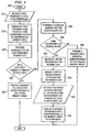
- FIGURE 4 The process by which the repair solution and map of failing memory locations can be generated is depicted in FIGURE 4 .
- the process starts (405) by first identifying three memory blocks in the embedded memory site that contain no failures (410). After this, the program generates a repair solution based upon the locations of the memory failures in the rest of the memory site (415). This repair solution is then stored in the first memory block that was identified as having no failures (420). In order to generate a shorthand notation of the location of the failing memory sites within the memory array, the program performs the following steps for each repairable memory block (425). First, the repairable memory block is copied into the third memory block that was identified as having no memory failures (430).
- This "image" of the repairable memory block is then used to generate the shorthand notation for the location of the specific memory failures.
- the following steps are performed (435). First, a new row tag is initialized in the second memory block that was identified as having no memory failures (440). Next, a word is read from the current row in the third memory site (a.k.a. the "image") (445). If there is not a failure within the word (450) then the process proceeds to the next word in the row (455). If, however, a failure is detected in the word, a bit in a subgroup ID corresponding to the location of the memory failure in the second memory block will be activated (460). After this, the process proceeds to the next word in the row (455).
- the process determines if any failures were found in the row that was just processed (470). If failures were found in the current row, then the process proceeds to the operations depicted in FIGURE 4A (475). If failures were not found in the current row, then the current row tag is removed from the second memory block (480) and the process proceeds to the next row in the memory block 485.
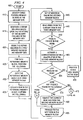
- the process will utilize the steps depicted in FIGURE 4A .
- the process begins by reading a bit from the subgroup ID (487). If the bit indicates a memory failure (489), then a corresponding word from the third memory block (i.e. the "image") will be retrieved (491). After this, the retrieved word is written into the second memory block (493). If, however, the bit does not indicate a memory failure (489) then these steps (491, 493) are bypassed. After this, the process proceeds to the next bit in the subgroup ID (495). Upon reaching the last bit in the subgroup ID (497) the process returns to step 485 depicted in Figure 4 .
Landscapes
- Techniques For Improving Reliability Of Storages (AREA)
- Tests Of Electronic Circuits (AREA)
- For Increasing The Reliability Of Semiconductor Memories (AREA)
- Test And Diagnosis Of Digital Computers (AREA)
- Microcomputers (AREA)
- Semiconductor Memories (AREA)
Claims (10)
- Ein Verfahren für die Selbstprüfung einer Vielzahl von eingebetteten Speicherorten (110-113), die auf einen Computerchip (100) gehaust werden, wobei jeder der eingebetteten Speicherorten sich mit einem Computerprozessor (105-108) assoziiert wird, der auch auf dem Computerchip gehaust wird, das Verfahren bestehend aus:dem Empfang (310) eines Programms zum Prüfen von einem außenen Prüfungsgerät bei einem Datenfluss-Steuergerät (115), das auf dem Computerchip (100) gehaust wird, das Datenfluss-Steuergerät verbundet mit jedem der eingebetteten Speicherorten (110-113);der Sendung (315) des Programms zum Prüfen von dem Datenfluss-Steuergerät zu jeder der Vielzahl von eingebetteten Speicherortern (110-113) auf dem Computerchip (100);der Ausführung gleichzeitig eines Programms zum Prüfen bei jedem der Computerprozessoren (105-108), wobei der Programm zum Prüfen einen Bestehen-, Versager- oder Reparaturzustand eines Speicherortes bestimmt, und erzeugt eine Reparaturlösung für jeden der reparierbaren Speicherorten, der Reparaturzustand zeigt einen reparierbaren versagten Speicherort;der Lieferung (330, 345, 365) eines Speicherzustandanzeigeteils, der jedem der Speicherorten entspricht, wobei der Speicherzustandanzeigeteil einen Bestehen-, Versager- oder Reparaturzustand des Speicherortes zeigt, der Reparaturzustand zeigt einen reparierbaren versagten Speicherort;dem Speichern (420) einer Reparaturlösung in einem ersten Block von bestehenden Speicher mit keinen Speicherorten mit einem Versagerzustand;für jeden der Speicherorten, der einen Reparaturzustand zeigt, die Abholung des ersten Blocks von Speicher, der der Reparaturlösung für die Speicherorten entspricht; und der Lieferung jede der abgeholten Reparaturlösungen von dem Datenfluss-Steuergerät zum außenen Prüfungsgerät.
- Ein Verfahren nach Anspruch 1, wobei die Ausführung eines Programms zum Prüfen dazu aus der Erzeugung (355) einer Karte von versagten Speicherorten für jeden der Speicherorten besteht, welcher Ort einen Versager- oder Reparaturzustand zeigt, das Verfahren dazu bestehend aus:für jeden der Speicherorten, der einen Reparatur-oder Versagerzustand zeigt, die Abholung eines zweiten Blocks von Speicher entsprechend der Karte von versagten Speicherorten; undder Bereitsstellung zu jeder der abgeholten Karten von versagten Speicheroten zu einem außenen Gerät zum Prüfen.
- Ein Verfahren nach Ansprüchen 1 oder 2, wobei das Verfahren von der Ausführung des Programms zum Prüfen besteht aus:der Ausführung eines ersten Teil des Programms zum Prüfen bei jedem der Computerprozessoren (105-108), wobei der ersten Teil des Programms zum Prüfen einen Funktionstest auf jedem der Speicherblocks in einem entsprechenden eingebetteten Speicherort ausführt;wenn mindestens drei Speicherblocks (410) den Funktionstest bei einem eingebetteten Speicherort bestehen, so wird die Folgende bei einem entsprechenden Speicherort ausgeführt:die Ausführung eines zweiten Teils des Programms zum Prüfen bei einem entsprechenden Computerprozessor, wobei der zweite Teil des Programms zum Prüfen einen Bestehen-, Versager- oder Reparaturzustand eines entpsrechenden Speicherortes bestimmt;wenn der Speicherort einen Reparaturzustand zeigt, dann wird einen dritten Teil des Programms zum Prüfen bei einem entsprechenden Computerprozessor ausgeführt, wobei der dritten Teil des Programms zum Prüfen eine Reparaturlösung eines entsprechenden eingebetteten Speicherort erzeugt (350; 415) und speichert (420) die Reparaturlösung in einem ersten Block von bestehenden Speicher; undwenn der Speicherort einen Reparatur-oder Versagerzustand zeigt, dann wird einen vierten Teil des Programms zum Prüfen bei einem entsprechenden Computerprozessor ausgeführt, wobei der vierte Teil des Programms zum Prüfen den dritten Block von bestehenden Speicher benutzt, um eine Karte der versagten Speicherorten zu erzeugen (355) und speichert die Karte in einem zweiten Block von bestehenden Speicher.
- Ein Verfahren nach Anspruch 3, wobei der Funktionstest aus der Folgenden besteht:wenn die ersten zwei Speicherblocks in einem entsprechenden eingebetteten Speicherort Versagern einschließen, dann wird einen Versagerzustand für den entsprechenden eingebetteten Speicherort gezeigt.
- Ein Verfahren nach allen vorhergehenden Ansprüchen, dazu bestehend aus:für jeden der Speicherorten, die einen Reparaturzustand zeigen, wird eine entsprechende Reparaturlösung ausgeführt, wobei bestimmten entlassenden Speicherzellen aktiviert werden und die Fehlerspeicherzellen deaktiviert werden.
- Ein Verfahren nach Anspruch 5, wobei die Aktivierung und Deaktivierung von Speicherzellen ein Fusionsverfahren benutzt.
- Eine integrierte Schaltung (100) betriebsfähig die Selbstprüfung einer Vielzahl von eingebetteten Speicherorten gleichzeitig auszuführen, die integrierte Schaltung bestehend aus:einer Vielzahl von eingebetteten Prozessoren (105-108) betriebsfähig um ein Speicherprüfensprogramm gleichzeitig auszuführen; und gekennzeichnet durcheine Vielzahl von eingebetteten Speicherorten (110-113), jeder davon entspricht einem der eingebetteten Prozessoren (105-108);einer Datenfluss-Steuereinheit (115) verbundet mit jedem der eingebetteten Speicherorten (110-113) und betriebsfähig, ein Speicherprüfensprogramm von einem außenen Testgerät zu empfangen und ein Speicherprüfensprogramm zu jedem der eingebetteten Speicherorten zu liefern;einer Vielzahl von Speicherzustandszeigeteilen (125-128), jeder davon entspricht einem der eingebetteten Speicherorten (110-113), wobei jeder der Speicherzustandszeigeteilen (125-128) betriebsfähig ist, einen Bestehen-, Versager- oder Reparaturzustand eines entsprechenden eingebetteten Speicherortes nach den Resultaten der Ausführung eines Teils des Speicherprüfensprogramms zu liefern, der Reparaturzustand zeigt einen reparierbaren versagten Speicherort,wobei das Datenfluss-Steuergerät (115) betriebsfähig ist, um eine von dem Speicherprüfensprogramms erzeugten Reparaturlösung für jeden der eingebetteten Speicherorten abzuholen, die einen Reparaturzustand zeigen, und eine Reparaturlösung zum außenen Testgerät zu liefern.
- Eine integrierte Schaltung nach Anspruch 7, wobei das Datenfluss-Steuergerät (115) dazu betriebsfähig ist, eine Karte der versagten Speicherorten abzuholen, die von dem Speicherprüfensprogramm von jedem der eingebetteten Speicherorten (110-113) erzeugt werden, die einen Reparatur-oder Versagerzustand zeigen, und die Karte von versagten Speicherorten zum außenen Testgerät zu liefern.
- Eine integrierte Schaltung nach Ansprüchen 7 oder 8, wobei die Datenfluss-Steuereinheit (115) dazu aus einem Hostportinterface besteht, das das außene Testgerät die Kommunikation mit jedem der eingebetteten Prozessoren (105-108) erlaubt.
- Eine integrierte Schaltung nach Ansprüchen 7-9, wobei die Datenfluss-Steuereinheit (115) dazu aus einem Strobegenerator und einem Strobeausgang (150) besteht, um Datentransfer von einem der eingebetteten Speicherorten (110-113) zum außenen Testgerät zu synchronisieren.
Applications Claiming Priority (4)
| Application Number | Priority Date | Filing Date | Title |
|---|---|---|---|
| US44394603P | 2003-01-31 | 2003-01-31 | |
| US443946P | 2003-01-31 | ||
| US10/425,410 US7155637B2 (en) | 2003-01-31 | 2003-04-29 | Method and apparatus for testing embedded memory on devices with multiple processor cores |
| US425410 | 2003-04-29 |
Publications (2)
| Publication Number | Publication Date |
|---|---|
| EP1447814A1 EP1447814A1 (de) | 2004-08-18 |
| EP1447814B1 true EP1447814B1 (de) | 2013-01-09 |
Family
ID=32685173
Family Applications (1)
| Application Number | Title | Priority Date | Filing Date |
|---|---|---|---|
| EP04100367A Expired - Lifetime EP1447814B1 (de) | 2003-01-31 | 2004-02-02 | Verfahren und Gerät zum Test eingebetteter Speicher von Geräten mit mehreren Prozessoren |
Country Status (3)
| Country | Link |
|---|---|
| US (1) | US7155637B2 (de) |
| EP (1) | EP1447814B1 (de) |
| JP (1) | JP2004233350A (de) |
Families Citing this family (35)
| Publication number | Priority date | Publication date | Assignee | Title |
|---|---|---|---|---|
| KR100543932B1 (ko) * | 2003-04-30 | 2006-01-23 | 주식회사 하이닉스반도체 | 초기화 동작시간이 감소된 태그블럭을 구비하는 반도체 메모리 장치 및 그의 구동방법 |
| DE10335708B4 (de) * | 2003-08-05 | 2009-02-26 | Qimonda Ag | Hub-Baustein zum Anschließen von einem oder mehreren Speicherbausteinen |
| US8516179B2 (en) * | 2003-12-03 | 2013-08-20 | Digital Rna, Llc | Integrated circuit with coupled processing cores |
| US7360130B2 (en) * | 2004-05-24 | 2008-04-15 | Jed Margolin | Memory with integrated programmable controller |
| US7380180B2 (en) * | 2004-07-16 | 2008-05-27 | Intel Corporation | Method, system, and apparatus for tracking defective cache lines |
| DE102004041822A1 (de) * | 2004-08-27 | 2006-03-02 | Robert Bosch Gmbh | Funktionseinheit zur Ausführung von logischen Testfällen auf einem an eine zu prüfende Einheit angekoppelten Testsystem und entsprechendes Verfahren |
| JP2006099232A (ja) * | 2004-09-28 | 2006-04-13 | Renesas Technology Corp | 半導体信号処理装置 |
| US20060117133A1 (en) * | 2004-11-30 | 2006-06-01 | Crowdsystems Corp | Processing system |
| US7603582B2 (en) * | 2005-02-18 | 2009-10-13 | Hewlett-Packard Development Company, L.P. | Systems and methods for CPU repair |
| US8667324B2 (en) * | 2005-02-18 | 2014-03-04 | Hewlett-Packard Development Company, L.P. | Systems and methods for CPU repair |
| US7917804B2 (en) * | 2005-02-18 | 2011-03-29 | Hewlett-Packard Development Company, L.P. | Systems and methods for CPU repair |
| US7523346B2 (en) * | 2005-02-18 | 2009-04-21 | Hewlett-Packard Development Company, L.P. | Systems and methods for CPU repair |
| US7607038B2 (en) | 2005-02-18 | 2009-10-20 | Hewlett-Packard Development Company, L.P. | Systems and methods for CPU repair |
| US7607040B2 (en) | 2005-02-18 | 2009-10-20 | Hewlett-Packard Development Company, L.P. | Methods and systems for conducting processor health-checks |
| US7694175B2 (en) * | 2005-02-18 | 2010-04-06 | Hewlett-Packard Development Company, L.P. | Methods and systems for conducting processor health-checks |
| US8661289B2 (en) * | 2005-02-18 | 2014-02-25 | Hewlett-Packard Development Company, L.P. | Systems and methods for CPU repair |
| US7673171B2 (en) | 2005-02-18 | 2010-03-02 | Hewlett-Packard Development Company, L.P. | Systems and methods for CPU repair |
| US7694174B2 (en) * | 2005-02-18 | 2010-04-06 | Hewlett-Packard Development Company, L.P. | Systems and methods for CPU repair |
| KR100691007B1 (ko) * | 2005-05-11 | 2007-03-09 | 주식회사 하이닉스반도체 | 메모리 장치의 테스트 방법 |
| US7818625B2 (en) * | 2005-08-17 | 2010-10-19 | Microsoft Corporation | Techniques for performing memory diagnostics |
| US7263642B1 (en) * | 2005-09-15 | 2007-08-28 | Azul Systems, Inc | Testing replicated sub-systems in a yield-enhancing chip-test environment using on-chip compare to expected results for parallel scan chains testing critical and repairable sections of each sub-system |
| US7401270B2 (en) * | 2005-10-20 | 2008-07-15 | Infineon Technologies Ag | Repair of semiconductor memory device via external command |
| US7647476B2 (en) * | 2006-03-14 | 2010-01-12 | Intel Corporation | Common analog interface for multiple processor cores |
| US9195628B2 (en) * | 2008-08-15 | 2015-11-24 | Intel Deutschland Gmbh | Partitioned bluetooth system |
| US8140902B2 (en) * | 2008-11-12 | 2012-03-20 | International Business Machines Corporation | Internally controlling and enhancing advanced test and characterization in a multiple core microprocessor |
| US8122312B2 (en) * | 2009-04-14 | 2012-02-21 | International Business Machines Corporation | Internally controlling and enhancing logic built-in self test in a multiple core microprocessor |
| NL2004392A (en) * | 2009-04-15 | 2010-10-18 | Asml Netherlands Bv | Lithographic apparatus, control system, multi-core processor, and a method to start tasks on a multi-core processor. |
| US9336105B2 (en) | 2010-09-30 | 2016-05-10 | International Business Machines Corporation | Evaluation of multiple input signature register results |
| KR101088588B1 (ko) * | 2010-12-03 | 2011-12-06 | 삼성전자주식회사 | 멀티 칩 패키지 테스트 장치 및 테스트 방법 |
| CN104461797B (zh) * | 2013-09-18 | 2017-07-21 | 达丰(上海)电脑有限公司 | 测试笔记本电脑外接显示接口的系统及方法 |
| US10198358B2 (en) * | 2014-04-02 | 2019-02-05 | Advanced Micro Devices, Inc. | System and method of testing processor units using cache resident testing |
| TWI569284B (zh) * | 2015-05-27 | 2017-02-01 | 慧榮科技股份有限公司 | 記憶體控制器與記憶體模組 |
| US9484116B1 (en) * | 2015-08-17 | 2016-11-01 | Advantest Corporation | Test system |
| US11211136B2 (en) * | 2019-06-26 | 2021-12-28 | Micron Technology, Inc. | Memory system tester using test pad real time monitoring |
| DE102022203166A1 (de) * | 2022-03-31 | 2023-10-05 | Robert Bosch Gesellschaft mit beschränkter Haftung | Verfahren zum Testen einer auf mehrere Programme verteilten Datenverarbeitung |
Family Cites Families (18)
| Publication number | Priority date | Publication date | Assignee | Title |
|---|---|---|---|---|
| US4191996A (en) * | 1977-07-22 | 1980-03-04 | Chesley Gilman D | Self-configurable computer and memory system |
| DE3728521A1 (de) * | 1987-08-26 | 1989-03-09 | Siemens Ag | Anordnung und verfahren zur feststellung und lokalisierung von fehlerhaften schaltkreisen eines speicherbausteins |
| EP1046994A3 (de) * | 1994-03-22 | 2000-12-06 | Hyperchip Inc. | Direkte Zellenersetzung für fehlertolerante Architektur mit gänzlich integrierten Systemen und mit Mitteln zur direkten Kommunikation mit Systembediener |
| US5748640A (en) * | 1996-09-12 | 1998-05-05 | Advanced Micro Devices | Technique for incorporating a built-in self-test (BIST) of a DRAM block with existing functional test vectors for a microprocessor |
| US5961653A (en) * | 1997-02-19 | 1999-10-05 | International Business Machines Corporation | Processor based BIST for an embedded memory |
| US5991898A (en) * | 1997-03-10 | 1999-11-23 | Mentor Graphics Corporation | Arithmetic built-in self test of multiple scan-based integrated circuits |
| KR100230454B1 (ko) | 1997-05-28 | 1999-11-15 | 윤종용 | 다중처리 시스템의 캐시메모리 검사방법 |
| US5995731A (en) | 1997-12-29 | 1999-11-30 | Motorola, Inc. | Multiple BIST controllers for testing multiple embedded memory arrays |
| KR20000009123A (ko) | 1998-07-21 | 2000-02-15 | 윤종용 | 초고속 구동용 슬롯리스 모터 |
| JP4587500B2 (ja) * | 1998-11-11 | 2010-11-24 | ルネサスエレクトロニクス株式会社 | 半導体集積回路、メモリモジュール、記憶媒体、及び半導体集積回路の救済方法 |
| US6374377B1 (en) | 1998-12-14 | 2002-04-16 | Intel Corporation | Low yield analysis of embedded memory |
| US6560740B1 (en) | 1999-08-03 | 2003-05-06 | Advanced Micro Devices, Inc. | Apparatus and method for programmable built-in self-test and self-repair of embedded memory |
| US6421283B1 (en) * | 2000-09-27 | 2002-07-16 | Conexant Systems, Inc. | Trap and patch system for virtual replacement of defective volatile memory cells |
| KR100374636B1 (ko) * | 2000-10-18 | 2003-03-04 | 삼성전자주식회사 | 결함 테스트 및 분석 회로를 구비하는 반도체 장치 및 결함 분석 방법 |
| JP2003059286A (ja) * | 2001-08-20 | 2003-02-28 | Mitsubishi Electric Corp | 半導体装置 |
| US6907548B2 (en) * | 2002-01-02 | 2005-06-14 | Intel Corporation | Automatic testing for multi-core architecture |
| US6865694B2 (en) * | 2002-04-30 | 2005-03-08 | Texas Instruments Incorporated | CPU-based system and method for testing embedded memory |
| JP2003324155A (ja) * | 2002-04-30 | 2003-11-14 | Mitsubishi Electric Corp | 半導体集積回路装置及びそのテスト方法 |
-
2003
- 2003-04-29 US US10/425,410 patent/US7155637B2/en not_active Expired - Lifetime
-
2004
- 2004-01-23 JP JP2004015692A patent/JP2004233350A/ja active Pending
- 2004-02-02 EP EP04100367A patent/EP1447814B1/de not_active Expired - Lifetime
Also Published As
| Publication number | Publication date |
|---|---|
| JP2004233350A (ja) | 2004-08-19 |
| EP1447814A1 (de) | 2004-08-18 |
| US7155637B2 (en) | 2006-12-26 |
| US20040153793A1 (en) | 2004-08-05 |
Similar Documents
| Publication | Publication Date | Title |
|---|---|---|
| EP1447814B1 (de) | Verfahren und Gerät zum Test eingebetteter Speicher von Geräten mit mehreren Prozessoren | |
| US7149924B1 (en) | Apparatus, method, and system having a pin to activate the self-test and repair instructions | |
| US11651831B2 (en) | Redundancy analysis circuit and memory system including the same | |
| JP2570203B2 (ja) | 半導体記憶装置 | |
| US7237154B1 (en) | Apparatus and method to generate a repair signature | |
| US6259637B1 (en) | Method and apparatus for built-in self-repair of memory storage arrays | |
| US7474575B2 (en) | Apparatus for testing a memory of an integrated circuit | |
| US20030204795A1 (en) | Testing of ECC memories | |
| JPH05205497A (ja) | アレイビルトインセルフテスト(abist)システム、半導体チップのビルトインセルフテストシステム、及びメモリアレイのテスト方法 | |
| US7930592B2 (en) | Enabling memory redundancy during testing | |
| US7137049B2 (en) | Method and apparatus for masking known fails during memory tests readouts | |
| KR19980041868A (ko) | 데이터 프로세싱 시스템 및 그 동작 방법 | |
| US6993692B2 (en) | Method, system and apparatus for aggregating failures across multiple memories and applying a common defect repair solution to all of the multiple memories | |
| US20060179368A1 (en) | Method and apparatus for providing flexible modular redundancy allocation for memory built in self test of SRAM with redundancy | |
| US7149941B2 (en) | Optimized ECC/redundancy fault recovery | |
| US20050066226A1 (en) | Redundant memory self-test | |
| US7016242B2 (en) | Semiconductor memory apparatus and self-repair method | |
| JP2003509804A (ja) | メモリ検査方法 | |
| US7596728B2 (en) | Built-in self repair circuit for a multi-port memory and method thereof | |
| JP4215723B2 (ja) | 集積回路 | |
| US6751762B2 (en) | Systems and methods for testing a memory | |
| US7549098B2 (en) | Redundancy programming for a memory device | |
| JP2002042485A (ja) | 半導体メモリ試験装置 | |
| JP2001101896A (ja) | 冗長回路への置換判定回路およびこれを含む半導体メモリ装置並びに半導体メモリ試験装置 | |
| US20070118778A1 (en) | Method and/or apparatus to detect and handle defects in a memory |
Legal Events
| Date | Code | Title | Description |
|---|---|---|---|
| PUAI | Public reference made under article 153(3) epc to a published international application that has entered the european phase |
Free format text: ORIGINAL CODE: 0009012 |
|
| AK | Designated contracting states |
Kind code of ref document: A1 Designated state(s): AT BE BG CH CY CZ DE DK EE ES FI FR GB GR HU IE IT LI LU MC NL PT RO SE SI SK TR |
|
| AX | Request for extension of the european patent |
Extension state: AL LT LV MK |
|
| 17P | Request for examination filed |
Effective date: 20050218 |
|
| AKX | Designation fees paid |
Designated state(s): DE FR GB |
|
| RBV | Designated contracting states (corrected) |
Designated state(s): DE FR GB |
|
| 17Q | First examination report despatched |
Effective date: 20091028 |
|
| REG | Reference to a national code |
Ref country code: DE Ref legal event code: R079 Ref document number: 602004040701 Country of ref document: DE Free format text: PREVIOUS MAIN CLASS: G11C0029000000 Ipc: G11C0029080000 |
|
| GRAP | Despatch of communication of intention to grant a patent |
Free format text: ORIGINAL CODE: EPIDOSNIGR1 |
|
| RIC1 | Information provided on ipc code assigned before grant |
Ipc: G11C 29/08 20060101AFI20120820BHEP |
|
| GRAS | Grant fee paid |
Free format text: ORIGINAL CODE: EPIDOSNIGR3 |
|
| GRAA | (expected) grant |
Free format text: ORIGINAL CODE: 0009210 |
|
| AK | Designated contracting states |
Kind code of ref document: B1 Designated state(s): DE FR GB |
|
| REG | Reference to a national code |
Ref country code: GB Ref legal event code: FG4D |
|
| REG | Reference to a national code |
Ref country code: DE Ref legal event code: R096 Ref document number: 602004040701 Country of ref document: DE Effective date: 20130307 |
|
| PLBE | No opposition filed within time limit |
Free format text: ORIGINAL CODE: 0009261 |
|
| STAA | Information on the status of an ep patent application or granted ep patent |
Free format text: STATUS: NO OPPOSITION FILED WITHIN TIME LIMIT |
|
| 26N | No opposition filed |
Effective date: 20131010 |
|
| REG | Reference to a national code |
Ref country code: DE Ref legal event code: R097 Ref document number: 602004040701 Country of ref document: DE Effective date: 20131010 |
|
| REG | Reference to a national code |
Ref country code: FR Ref legal event code: PLFP Year of fee payment: 13 |
|
| REG | Reference to a national code |
Ref country code: FR Ref legal event code: PLFP Year of fee payment: 14 |
|
| REG | Reference to a national code |
Ref country code: FR Ref legal event code: PLFP Year of fee payment: 15 |
|
| PGFP | Annual fee paid to national office [announced via postgrant information from national office to epo] |
Ref country code: GB Payment date: 20190128 Year of fee payment: 16 Ref country code: DE Payment date: 20190115 Year of fee payment: 16 Ref country code: FR Payment date: 20190117 Year of fee payment: 16 |
|
| REG | Reference to a national code |
Ref country code: DE Ref legal event code: R119 Ref document number: 602004040701 Country of ref document: DE |
|
| GBPC | Gb: european patent ceased through non-payment of renewal fee |
Effective date: 20200202 |
|
| PG25 | Lapsed in a contracting state [announced via postgrant information from national office to epo] |
Ref country code: FR Free format text: LAPSE BECAUSE OF NON-PAYMENT OF DUE FEES Effective date: 20200229 Ref country code: GB Free format text: LAPSE BECAUSE OF NON-PAYMENT OF DUE FEES Effective date: 20200202 Ref country code: DE Free format text: LAPSE BECAUSE OF NON-PAYMENT OF DUE FEES Effective date: 20200901 |