EP1447847A2 - Leiterrahmen für ein Gehäuse eines elektronischen Bauelementes - Google Patents
Leiterrahmen für ein Gehäuse eines elektronischen Bauelementes Download PDFInfo
- Publication number
- EP1447847A2 EP1447847A2 EP04250482A EP04250482A EP1447847A2 EP 1447847 A2 EP1447847 A2 EP 1447847A2 EP 04250482 A EP04250482 A EP 04250482A EP 04250482 A EP04250482 A EP 04250482A EP 1447847 A2 EP1447847 A2 EP 1447847A2
- Authority
- EP
- European Patent Office
- Prior art keywords
- lead
- frame
- rails
- fingers
- partially etched
- Prior art date
- Legal status (The legal status is an assumption and is not a legal conclusion. Google has not performed a legal analysis and makes no representation as to the accuracy of the status listed.)
- Withdrawn
Links
Images

Classifications
-
- H—ELECTRICITY
- H10—SEMICONDUCTOR DEVICES; ELECTRIC SOLID-STATE DEVICES NOT OTHERWISE PROVIDED FOR
- H10W—GENERIC PACKAGES, INTERCONNECTIONS, CONNECTORS OR OTHER CONSTRUCTIONAL DETAILS OF DEVICES COVERED BY CLASS H10
- H10W74/00—Encapsulations, e.g. protective coatings
- H10W74/10—Encapsulations, e.g. protective coatings characterised by their shape or disposition
- H10W74/111—Encapsulations, e.g. protective coatings characterised by their shape or disposition the semiconductor body being completely enclosed
-
- H—ELECTRICITY
- H10—SEMICONDUCTOR DEVICES; ELECTRIC SOLID-STATE DEVICES NOT OTHERWISE PROVIDED FOR
- H10W—GENERIC PACKAGES, INTERCONNECTIONS, CONNECTORS OR OTHER CONSTRUCTIONAL DETAILS OF DEVICES COVERED BY CLASS H10
- H10W70/00—Package substrates; Interposers; Redistribution layers [RDL]
- H10W70/40—Leadframes
- H10W70/421—Shapes or dispositions
- H10W70/424—Cross-sectional shapes
-
- H—ELECTRICITY
- H10—SEMICONDUCTOR DEVICES; ELECTRIC SOLID-STATE DEVICES NOT OTHERWISE PROVIDED FOR
- H10W—GENERIC PACKAGES, INTERCONNECTIONS, CONNECTORS OR OTHER CONSTRUCTIONAL DETAILS OF DEVICES COVERED BY CLASS H10
- H10W74/00—Encapsulations, e.g. protective coatings
- H10W74/01—Manufacture or treatment
- H10W74/016—Manufacture or treatment using moulds
-
- H—ELECTRICITY
- H10—SEMICONDUCTOR DEVICES; ELECTRIC SOLID-STATE DEVICES NOT OTHERWISE PROVIDED FOR
- H10W—GENERIC PACKAGES, INTERCONNECTIONS, CONNECTORS OR OTHER CONSTRUCTIONAL DETAILS OF DEVICES COVERED BY CLASS H10
- H10W72/00—Interconnections or connectors in packages
- H10W72/01—Manufacture or treatment
- H10W72/0198—Manufacture or treatment batch processes
-
- H—ELECTRICITY
- H10—SEMICONDUCTOR DEVICES; ELECTRIC SOLID-STATE DEVICES NOT OTHERWISE PROVIDED FOR
- H10W—GENERIC PACKAGES, INTERCONNECTIONS, CONNECTORS OR OTHER CONSTRUCTIONAL DETAILS OF DEVICES COVERED BY CLASS H10
- H10W72/00—Interconnections or connectors in packages
- H10W72/071—Connecting or disconnecting
- H10W72/075—Connecting or disconnecting of bond wires
-
- H—ELECTRICITY
- H10—SEMICONDUCTOR DEVICES; ELECTRIC SOLID-STATE DEVICES NOT OTHERWISE PROVIDED FOR
- H10W—GENERIC PACKAGES, INTERCONNECTIONS, CONNECTORS OR OTHER CONSTRUCTIONAL DETAILS OF DEVICES COVERED BY CLASS H10
- H10W72/00—Interconnections or connectors in packages
- H10W72/50—Bond wires
- H10W72/551—Materials of bond wires
-
- H—ELECTRICITY
- H10—SEMICONDUCTOR DEVICES; ELECTRIC SOLID-STATE DEVICES NOT OTHERWISE PROVIDED FOR
- H10W—GENERIC PACKAGES, INTERCONNECTIONS, CONNECTORS OR OTHER CONSTRUCTIONAL DETAILS OF DEVICES COVERED BY CLASS H10
- H10W72/00—Interconnections or connectors in packages
- H10W72/90—Bond pads, in general
- H10W72/951—Materials of bond pads
-
- H—ELECTRICITY
- H10—SEMICONDUCTOR DEVICES; ELECTRIC SOLID-STATE DEVICES NOT OTHERWISE PROVIDED FOR
- H10W—GENERIC PACKAGES, INTERCONNECTIONS, CONNECTORS OR OTHER CONSTRUCTIONAL DETAILS OF DEVICES COVERED BY CLASS H10
- H10W74/00—Encapsulations, e.g. protective coatings
-
- H—ELECTRICITY
- H10—SEMICONDUCTOR DEVICES; ELECTRIC SOLID-STATE DEVICES NOT OTHERWISE PROVIDED FOR
- H10W—GENERIC PACKAGES, INTERCONNECTIONS, CONNECTORS OR OTHER CONSTRUCTIONAL DETAILS OF DEVICES COVERED BY CLASS H10
- H10W74/00—Encapsulations, e.g. protective coatings
- H10W74/10—Encapsulations, e.g. protective coatings characterised by their shape or disposition
- H10W74/111—Encapsulations, e.g. protective coatings characterised by their shape or disposition the semiconductor body being completely enclosed
- H10W74/127—Encapsulations, e.g. protective coatings characterised by their shape or disposition the semiconductor body being completely enclosed characterised by arrangements for sealing or adhesion
-
- H—ELECTRICITY
- H10—SEMICONDUCTOR DEVICES; ELECTRIC SOLID-STATE DEVICES NOT OTHERWISE PROVIDED FOR
- H10W—GENERIC PACKAGES, INTERCONNECTIONS, CONNECTORS OR OTHER CONSTRUCTIONAL DETAILS OF DEVICES COVERED BY CLASS H10
- H10W90/00—Package configurations
- H10W90/701—Package configurations characterised by the relative positions of pads or connectors relative to package parts
- H10W90/751—Package configurations characterised by the relative positions of pads or connectors relative to package parts of bond wires
- H10W90/756—Package configurations characterised by the relative positions of pads or connectors relative to package parts of bond wires between a chip and a stacked lead frame, conducting package substrate or heat sink
Definitions
- This invention relates to the packaging of electronic components and more particularly but not solely to the packaging of semiconductor components.
- Traditional electronic components comprise a body which houses the active or passive electronic device and a plurality of projecting leads for connecting the device to relevant terminals on a printed circuit board.
- quad flat non-leaded component packages in which the projecting leads are replaced by conductive pads formed on the underside of the body of the component. It will be appreciated that the lack of projecting leads reduces the overall size of the component.
- Leadless electronic components are formed by die bonding the component device on a die pad of a metal lead-frame and then connecting the device with wire to terminals formed integrally on the frame by a process known as wire bonding.
- the upper surface of the lead-frame is then encapsulated to form a solid block that protects the device and wires, and has the conductive terminals exposed on its underside.
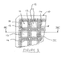
- a typical lead-frame assembly for a quad flat non-leaded package comprises a one-piece lead-frame 10 formed of a sheet of copper having an array of sites 11 for respectively receiving the individual component devices 15.
- a grid of rails 12 is formed on the lead-frame 10, with each site 11 occupying one space within the grid.
- Each site 11 comprises a central die pad 13 surrounded on its four sides by radially extending terminals or so-called lead-fingers 14, which are solely connected to the rails 12 of the lead-frame 10 at their radially outer ends.
- the individual component devices 15 are die-bonded to the upper surface of the die pads 13 of respective sites 11 and then the contact pads on the devices 15 are wired to respective lead-fingers 14 of the site 11 by a thermosonic bonding apparatus, which is programmed to bond one end of a fine wire 16 to a conductive pad on the component device 15 and then to draw the wire 16 out through a ceramic capillary to a lead-finger 14 on the lead-frame 10, where it is again bonded. This process is then repeated for each connection to be made between the conductive pads on the component device 15 and the lead-fingers 14 of the lead-frame 10.
- the upper surface of the assembly is then encapsulated in block of resin 17, which extends through the openings 18 in the lead-frame 10 and comprises an undersurface lying in the same plane as the undersurface of the lead-frame 10.
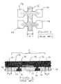
- the lead-frame assembly is singulated to form individual electronic components C by cutting along the rails 12 using a saw of a width W which is slightly wider than the width of the rails 12, as shown in Figures 2 and 3. In this manner, the adjacent lead-fingers 14 of each singulated component C are electrically isolated from each other.
- a disadvantage of the aforementioned method of singulation is that the saw causes undesirable burrs along the cut edges of the lead-fingers 14.
- a disadvantage of the above-mentioned solution to the problem of burring is that it substantially weakens the rails 12, with the result that difficulties are encountered when wire bonding the connecting wires 16 to the lead-fingers 14:
- the pressure with which the wire 16 is bonded to the lead-fingers 14 is crucial, since an over pressure can damage the lead-fingers 14 and an under pressure can result in an unsatisfactory bond.
- the thermal and electrical conductivity of the lead-fingers 14 and the supporting rails 12 affects the reliability of the bond.
- the bond parameters of the apparatus are difficult and time consuming to set up and can vary greatly between each lead-frame.
- a lead-frame formed of a sheet of metal, the lead-frame comprising an array of sites for receiving respective electronic component devices on the upper surface of the frame, a plurality of rails arranged in a grid, with each site being disposed in respective regions within of the grid, at least some of the rails carrying lead-fingers which project into respective sites, wherein the lower surface of the frame is partially etched over regions disposed at the points where the lead-fingers meet the rails, a strengthening region extending medially along each rail and having a thickness which is greater than the thickness of the partially etched regions.
- the lead-frame assembly is singulated to form individual electronic components by cutting along the rails using a saw which is slightly wider than the width of the rails. In this manner, the edges of the saw cut through partially etched regions at the points where the lead-fingers meet the rails. These partially etched regions are bounded on both their upper and lower sides by the resin encapsulation material and thus burring of the cut lead-fingers is avoided: Burring only occurs if you cut through an area of full thickness copper. When it is half etched, the edge that would burr is surrounded by the resin encapsulation material, which stops the burr occurring as the exit of the saw blade from the component is through compound and not copper.
- the strengthening region extending medially along each rail strengthens the rail and thus prevent the rail from flexing unduly under the applied pressure during wire bonding.
- the bond parameters of the apparatus are therefore not as difficult and time consuming to set up.
- the strengthening region on each rail is unetched.
- the lower surface of the lead-frame is partially etched over regions extending along lateral edges of the rails from which the lead-fingers extend, said partially etched regions extending partially into the lead-fingers.
- An advantage of half-etching the underside of the lateral side edges of the rails is that the saw is less prone to wear, since the saw has to cut through less metal as it passes along the rails.
- lead-fingers are provided on opposite sides of rails bounding adjacent sites, said bounding rails being partially etched along opposite lateral side edges, an unetched medial portion extending longitudinally along said bounding rails.
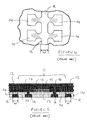
- the underside of the rails 12 carrying lead-fingers 14 are partially etched in regions R1, R2 extending along their lateral side edges, with the partially etched regions R1, R2 extending partially into the lead-fingers 14.
- the unetched medial portion M of the partially etched rails 12 has an undersurface which lies in the same plane as the undersurface of the lead-frame 10, as represented by the shading in Figure 6.
- the unetched medial portion M extending along each rail acts to strengthen the rail and thus prevents the rail from flexing unduly under the applied pressure during wire bonding.
- the bond parameters of the apparatus are therefore not as difficult and time consuming to set up as conventional partially etched lead-frames.
Landscapes
- Lead Frames For Integrated Circuits (AREA)
Applications Claiming Priority (2)
| Application Number | Priority Date | Filing Date | Title |
|---|---|---|---|
| GB0303285 | 2003-02-13 | ||
| GBGB0303285.1A GB0303285D0 (en) | 2003-02-13 | 2003-02-13 | Electronic component packaging |
Publications (2)
| Publication Number | Publication Date |
|---|---|
| EP1447847A2 true EP1447847A2 (de) | 2004-08-18 |
| EP1447847A3 EP1447847A3 (de) | 2004-09-29 |
Family
ID=9952939
Family Applications (1)
| Application Number | Title | Priority Date | Filing Date |
|---|---|---|---|
| EP04250482A Withdrawn EP1447847A3 (de) | 2003-02-13 | 2004-01-29 | Leiterrahmen für ein Gehäuse eines elektronischen Bauelementes |
Country Status (2)
| Country | Link |
|---|---|
| EP (1) | EP1447847A3 (de) |
| GB (1) | GB0303285D0 (de) |
Cited By (3)
| Publication number | Priority date | Publication date | Assignee | Title |
|---|---|---|---|---|
| JP2007258590A (ja) * | 2006-03-24 | 2007-10-04 | Disco Abrasive Syst Ltd | パッケージ基板の分割方法 |
| CN115547969A (zh) * | 2021-06-30 | 2022-12-30 | 意法半导体股份有限公司 | 制造半导体器件的方法、对应的基板和半导体器件 |
| US12557669B2 (en) | 2021-06-30 | 2026-02-17 | Stmicroelectronics S.R.L. | Method of manufacturing semiconductor devices, corresponding substrate and semiconductor device |
Family Cites Families (6)
| Publication number | Priority date | Publication date | Assignee | Title |
|---|---|---|---|---|
| US5202577A (en) * | 1990-02-06 | 1993-04-13 | Dai Nippon Printing Co., Ltd. | Leadframe having a particular dam bar |
| JP2001077287A (ja) * | 1999-09-06 | 2001-03-23 | Mitsubishi Electric Corp | 半導体装置用リードフレーム |
| JP2001320007A (ja) * | 2000-05-09 | 2001-11-16 | Dainippon Printing Co Ltd | 樹脂封止型半導体装置用フレーム |
| JP3443799B2 (ja) * | 2000-07-04 | 2003-09-08 | 株式会社三井ハイテック | 半導体装置の切出し方法及び装置 |
| JP2003086750A (ja) * | 2001-09-11 | 2003-03-20 | Rohm Co Ltd | 電子部品の製造方法 |
| JP2004023007A (ja) * | 2002-06-20 | 2004-01-22 | Sony Corp | 半導体パッケージ用リードフレーム及び半導体パッケージ並びに半導体パッケージの製造方法。 |
-
2003
- 2003-02-13 GB GBGB0303285.1A patent/GB0303285D0/en not_active Ceased
-
2004
- 2004-01-29 EP EP04250482A patent/EP1447847A3/de not_active Withdrawn
Cited By (3)
| Publication number | Priority date | Publication date | Assignee | Title |
|---|---|---|---|---|
| JP2007258590A (ja) * | 2006-03-24 | 2007-10-04 | Disco Abrasive Syst Ltd | パッケージ基板の分割方法 |
| CN115547969A (zh) * | 2021-06-30 | 2022-12-30 | 意法半导体股份有限公司 | 制造半导体器件的方法、对应的基板和半导体器件 |
| US12557669B2 (en) | 2021-06-30 | 2026-02-17 | Stmicroelectronics S.R.L. | Method of manufacturing semiconductor devices, corresponding substrate and semiconductor device |
Also Published As
| Publication number | Publication date |
|---|---|
| EP1447847A3 (de) | 2004-09-29 |
| GB0303285D0 (en) | 2003-03-19 |
Similar Documents
| Publication | Publication Date | Title |
|---|---|---|
| US8058104B2 (en) | Reversible leadless package and methods of making and using same | |
| US6927483B1 (en) | Semiconductor package exhibiting efficient lead placement | |
| US6818973B1 (en) | Exposed lead QFP package fabricated through the use of a partial saw process | |
| US7579674B2 (en) | Semiconductor package configuration with improved lead portion arrangement | |
| US8441110B1 (en) | Side leaded, bottom exposed pad and bottom exposed lead fusion quad flat semiconductor package | |
| US8575742B1 (en) | Semiconductor device with increased I/O leadframe including power bars | |
| US8432023B1 (en) | Increased I/O leadframe and semiconductor device including same | |
| US20100013069A1 (en) | Semiconductor device, lead frame and method of manufacturing semiconductor device | |
| US20080283980A1 (en) | Lead frame for semiconductor package | |
| US9363901B2 (en) | Making a plurality of integrated circuit packages | |
| CN111312682B (zh) | 紧凑型引线框封装件 | |
| US10090228B1 (en) | Semiconductor device with leadframe configured to facilitate reduced burr formation | |
| KR20160006608A (ko) | 리드 프레임, 반도체 장치, 및 리드 프레임의 제조 방법 | |
| US7410835B2 (en) | Method for fabricating semiconductor package with short-prevented lead frame | |
| US6692991B2 (en) | Resin-encapsulated semiconductor device and method for manufacturing the same | |
| CN100541748C (zh) | 引线框架、半导体芯片封装、及该封装的制造方法 | |
| US6696749B1 (en) | Package structure having tapering support bars and leads | |
| US20090206459A1 (en) | Quad flat non-leaded package structure | |
| USRE43818E1 (en) | Fabrication of an integrated circuit package | |
| EP1447847A2 (de) | Leiterrahmen für ein Gehäuse eines elektronischen Bauelementes | |
| EP1856738A1 (de) | Integrierte schaltungseinrichtungskapselung mit zusätzlicher kontaktstelle, anschlusskamm und elektronische einrichtung | |
| WO2007018473A1 (en) | Leadframe and semiconductor package | |
| KR20020093250A (ko) | 리드 노출형 리드 프레임 및 그를 이용한 리드 노출형반도체 패키지 | |
| US20240055327A1 (en) | Pre-plated lead tip for wettable flank leadframe | |
| KR100819794B1 (ko) | 리드프레임 및, 그것을 이용한 반도체 패키지 제조 방법 |
Legal Events
| Date | Code | Title | Description |
|---|---|---|---|
| PUAI | Public reference made under article 153(3) epc to a published international application that has entered the european phase |
Free format text: ORIGINAL CODE: 0009012 |
|
| PUAL | Search report despatched |
Free format text: ORIGINAL CODE: 0009013 |
|
| AK | Designated contracting states |
Kind code of ref document: A2 Designated state(s): AT BE BG CH CY CZ DE DK EE ES FI FR GB GR HU IE IT LI LU MC NL PT RO SE SI SK TR |
|
| AX | Request for extension of the european patent |
Extension state: AL LT LV MK |
|
| AK | Designated contracting states |
Kind code of ref document: A3 Designated state(s): AT BE BG CH CY CZ DE DK EE ES FI FR GB GR HU IE IT LI LU MC NL PT RO SE SI SK TR |
|
| AX | Request for extension of the european patent |
Extension state: AL LT LV MK |
|
| 17P | Request for examination filed |
Effective date: 20050115 |
|
| AKX | Designation fees paid |
Designated state(s): AT BE BG CH CY CZ DE DK EE ES FI FR GB GR HU IE IT LI LU MC NL PT RO SE SI SK TR |
|
| 17Q | First examination report despatched |
Effective date: 20060208 |
|
| STAA | Information on the status of an ep patent application or granted ep patent |
Free format text: STATUS: THE APPLICATION IS DEEMED TO BE WITHDRAWN |
|
| 18D | Application deemed to be withdrawn |
Effective date: 20080801 |