EP1447904A2 - Méthode et appareil puor la suppression de surtensions dans un onduleur à modulation de largeur d'impulsion - Google Patents
Méthode et appareil puor la suppression de surtensions dans un onduleur à modulation de largeur d'impulsion Download PDFInfo
- Publication number
- EP1447904A2 EP1447904A2 EP04002804A EP04002804A EP1447904A2 EP 1447904 A2 EP1447904 A2 EP 1447904A2 EP 04002804 A EP04002804 A EP 04002804A EP 04002804 A EP04002804 A EP 04002804A EP 1447904 A2 EP1447904 A2 EP 1447904A2
- Authority
- EP
- European Patent Office
- Prior art keywords
- pulse
- duration
- firing
- initial
- firing pulse
- Prior art date
- Legal status (The legal status is an assumption and is not a legal conclusion. Google has not performed a legal analysis and makes no representation as to the accuracy of the status listed.)
- Granted
Links
- 238000000034 method Methods 0.000 title claims abstract description 74
- 230000001629 suppression Effects 0.000 title 1
- 238000010304 firing Methods 0.000 claims abstract description 307
- 239000002131 composite material Substances 0.000 claims abstract description 53
- 239000003607 modifier Substances 0.000 claims description 34
- 230000008569 process Effects 0.000 abstract description 10
- 238000001228 spectrum Methods 0.000 description 7
- 230000000694 effects Effects 0.000 description 4
- 238000012986 modification Methods 0.000 description 4
- 230000004048 modification Effects 0.000 description 4
- 238000004804 winding Methods 0.000 description 4
- 238000013461 design Methods 0.000 description 3
- 230000002411 adverse Effects 0.000 description 2
- 230000004075 alteration Effects 0.000 description 2
- 238000010586 diagram Methods 0.000 description 2
- 238000010438 heat treatment Methods 0.000 description 2
- 238000012545 processing Methods 0.000 description 2
- 238000009825 accumulation Methods 0.000 description 1
- 238000004364 calculation method Methods 0.000 description 1
- 238000012937 correction Methods 0.000 description 1
- 230000001419 dependent effect Effects 0.000 description 1
- 230000008030 elimination Effects 0.000 description 1
- 238000003379 elimination reaction Methods 0.000 description 1
- 238000003475 lamination Methods 0.000 description 1
- 230000007246 mechanism Effects 0.000 description 1
- 238000005096 rolling process Methods 0.000 description 1
- 239000004065 semiconductor Substances 0.000 description 1
Images


Classifications
-
- H—ELECTRICITY
- H02—GENERATION; CONVERSION OR DISTRIBUTION OF ELECTRIC POWER
- H02M—APPARATUS FOR CONVERSION BETWEEN AC AND AC, BETWEEN AC AND DC, OR BETWEEN DC AND DC, AND FOR USE WITH MAINS OR SIMILAR POWER SUPPLY SYSTEMS; CONVERSION OF DC OR AC INPUT POWER INTO SURGE OUTPUT POWER; CONTROL OR REGULATION THEREOF
- H02M1/00—Details of apparatus for conversion
- H02M1/32—Means for protecting converters other than automatic disconnection
-
- H—ELECTRICITY
- H02—GENERATION; CONVERSION OR DISTRIBUTION OF ELECTRIC POWER
- H02M—APPARATUS FOR CONVERSION BETWEEN AC AND AC, BETWEEN AC AND DC, OR BETWEEN DC AND DC, AND FOR USE WITH MAINS OR SIMILAR POWER SUPPLY SYSTEMS; CONVERSION OF DC OR AC INPUT POWER INTO SURGE OUTPUT POWER; CONTROL OR REGULATION THEREOF
- H02M7/00—Conversion of AC power input into DC power output; Conversion of DC power input into AC power output
- H02M7/42—Conversion of DC power input into AC power output without possibility of reversal
- H02M7/44—Conversion of DC power input into AC power output without possibility of reversal by static converters
- H02M7/48—Conversion of DC power input into AC power output without possibility of reversal by static converters using discharge tubes with control electrode or semiconductor devices with control electrode
- H02M7/53—Conversion of DC power input into AC power output without possibility of reversal by static converters using discharge tubes with control electrode or semiconductor devices with control electrode using devices of a triode or transistor type requiring continuous application of a control signal
- H02M7/537—Conversion of DC power input into AC power output without possibility of reversal by static converters using discharge tubes with control electrode or semiconductor devices with control electrode using devices of a triode or transistor type requiring continuous application of a control signal using semiconductor devices only, e.g. single switched pulse inverters
- H02M7/5387—Conversion of DC power input into AC power output without possibility of reversal by static converters using discharge tubes with control electrode or semiconductor devices with control electrode using devices of a triode or transistor type requiring continuous application of a control signal using semiconductor devices only, e.g. single switched pulse inverters in a bridge configuration
- H02M7/53871—Conversion of DC power input into AC power output without possibility of reversal by static converters using discharge tubes with control electrode or semiconductor devices with control electrode using devices of a triode or transistor type requiring continuous application of a control signal using semiconductor devices only, e.g. single switched pulse inverters in a bridge configuration with automatic control of output voltage or current
- H02M7/53875—Conversion of DC power input into AC power output without possibility of reversal by static converters using discharge tubes with control electrode or semiconductor devices with control electrode using devices of a triode or transistor type requiring continuous application of a control signal using semiconductor devices only, e.g. single switched pulse inverters in a bridge configuration with automatic control of output voltage or current with analogue control of three-phase output
Definitions
- the present invention relates to motor controllers and more particularly, to a method and an apparatus for altering stator winding voltages to eliminate greater than twice over voltage.
- ASD Adjustable Speed Drive
- PWM Pulse Width Modulated
- a three-phase PWM controller receives three reference or modulating signals and a triangle carrier signal, compares each modulating signal to the carrier signal and generates firing signals consisting of a plurality of pulses corresponding to each modulating signal.
- a modulating signal has a greater instantaneous amplitude than the carrier signal, a corresponding firing signal is high producing a pulse on-time.
- a modulating signal has an instantaneous amplitude that is less than the carrier signal, a corresponding firing signal is low producing a pulse off-time.
- a three-phase PWM inverter consists of three pairs of switches, each switch pair including series arranged upper and lower switches configured between positive and negative DC power supplies. Each pair of switches is linked to a unique motor terminal by a unique supply line, each supply line is connected to a node between an associated pair of switches. Each firing signal controls an associated switch pair to alternately connect a stator winding between the positive and negative DC power supplies to produce a series of high frequency voltage pulses that resemble the firing signals.
- a changing average of the high frequency voltage pulses over a period defines a fundamental low frequency alternating line-to-line voltage between motor terminals that drives the motor.
- IGBTs Insulated Gate Bipolar Transistors
- PWM inverter PWM inverter
- IGBTs have fast rise times and associated switching speeds (e.g. 50-400 ns) that are at least an order of magnitude faster than BJTs and other similar devices.
- switching speeds switching frequency and efficiency, and the quality of terminal voltages, are all appreciably improved.
- the faster switching speeds reduce harmonic heating of the motor winding as well as reduce audible motor lamination noise.
- IGBT PWMs are advantageous for all of the reasons identified above, when combined with certain switch modulating techniques (i.e. certain on/off switching sequences), IGBT fast dv/dt or rise times can reduce the useful life of motor components and/or drive to motor voltage supply lines.
- switch modulating techniques i.e. certain on/off switching sequences
- IGBT fast dv/dt or rise times can reduce the useful life of motor components and/or drive to motor voltage supply lines.
- fast switch rise times causes overvoltages that exceed design levels.
- twice overvoltage i.e. twice the PWM inverter DC power supply level
- twice overvoltage levels are caused by various combinations of line voltage rise time and magnitude, imperfect matches between line-to-line supply cable and motor surge impedances, and cable length. Line voltage frequency and switch modulating techniques have little effect on twice overvoltage levels.
- the second overvoltage problem is referred to herein as greater than twice overvoltage. Unlike twice overvoltage, greater than twice overvoltage is caused by faster IGBT switching frequencies and faster IGBT dv/dt rise times interacting with two different common switch modulating techniques, that result in overvoltage problems referred to as "double pulsing" and "polarity reversal".
- One other solution to mitigate the adverse effects of rise time induced motor overvoltages has been to modify modulation and commutation software.
- Some of the more sophisticated techniques of this type include providing a motor controller that modifies firing pulses that are provided to an inverter in a manner calculated to eliminate greater than twice overvoltage switching sequences. When the period between two voltage changes is less than the period required for a substantially steady state voltage near zero to be reached, the period between the two voltage changes is increased. Where switching sequence results in greater than twice overvoltage due to polarity reversal, the switching sequence is altered to eliminate the possibility of greater than twice overvoltage.
- MMPT Maximum-Minimum Pulse Technique
- PET Pulse Elimination Technique
- some of the pulses having characteristics which could generate greater than twice overvoltage are eliminated.
- some of the positive pulse durations during positive half cycles are increased and set equal to the carrier period and some of the negative pulse durations during negative half cycles are increased and set equal to the carrier period.
- the result is a terminal voltage magnitude which is essentially unaffected by pulse alterations.
- the terminal voltage magnitude is noticeably reduced as some positive pulse durations during positive half cycles and some negative pulse durations during negative half cycles are reduced.
- the terminal voltage magnitude is noticeably increased as some positive pulse durations during positive half cycles and some negative pulse durations during negative half cycles are increased.
- One way to deal with errors caused by MMPT and PET methods is to provide feedback loops in the control system.
- one control system including a feedback loop has been operated with an 18 microsecond dwell time and a carrier frequency of between 1 and 12 kHz with insignificant distortion.
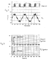
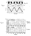
- Fig. 1 a U-phase to positive bus voltage signal and resulting U-phase current waveform are illustrated that were generated using a controller employing a two phase discontinuous modulating waveform at 55 Hz with a 630 V bus, a carrier frequency of 4 kHz and a dwell time of ten microseconds.
- Fig. 1 clearly shows that the current waveform is distorted despite the fact that the corrective code for dealing with the reflected wave phenomenon has been activated.
- Fig. 2 illustrates the frequency spectra for voltage U-phase to positive bus voltage and the U-phase current. Flattening of the current peak in Fig. 1 is consistent with the current spectrum of Fig. 2 where the 5th harmonic is approximately 0.5 Arms and he 7th harmonic is approximately 0.25 Arms.
- the voltage spectrum in Fig. 2 includes voltage components at the 5th and 7th harmonics and a common mode component - the 2nd harmonic component illustrated.
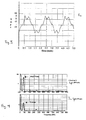
- Fig. 3 includes a current waveform l u similar to the current waveform of Fig. 1, except that the carrier frequency and dwell time used to generate the waveform of Fig. 3 where 8 kHz and 8 microseconds, respectively (the decrease in dwell time was necessary because of stability and distortion requirements).
- the current distortion is appreciably increased.
- the primary cause of the increased distortion is that the dwell time percent voltage increases as carrier frequency is increased.
- Fig. 4 is similar to Fig. 2 except that the spectrum of Fig. 4 correspond to a U-phase to positive bus voltage signal (not illustrated) generated with a carrier frequency and a dwell time of 8 kHz and 8 micro seconds, respectively, and the U-phase current waveform of Fig. 3.
- the magnitudes of the distorting harmonics are increased appreciably.
- controller designers are confronted with selecting among different control options and accepting various tradeoffs.
- tradeoffs are current distortion vs. execution time and voltage feedback/speed range vs. cost.
- the invention includes a method to be used with a motor controller generating firing pulses to control an inverter, the inverter providing exciting voltage to a motor corresponding to the firing pulses, the voltage having a maximum intended amplitude, the method for substantially eliminating exciting voltage overvoltage by modifying the firing pulses, the method comprising the steps of (a)identifying characteristics of an initial firing pulse, (b)comparing the initial pulse characteristics to an overvoltage characteristic set known to cause overvoltage, (c)where the initial pulse characteristics match the overvoltage characteristic set, altering the initial firing pulse such that the altered firing pulse does not cause overvoltage, (d)identifying an accumulated error corresponding to the modified firing pulse, (e)modifying the firing pulse following the altered firing pulse as a function of the accumulated error to generate a composite firing pulse; and (f) repeating steps (a) through (e) with the composite firing pulse as the initial firing pulse.
- the step of identifying the accumulated error includes identifying the difference between the initial firing pulse and the altered firing pulse. In some embodiments the step of modifying the firing pulse includes adding the accumulated error to the pulse following the altered firing pulse.
- the controller includes a comparator that compares a reference signal to a carrier signal to provide the following firing pulses, one following firing pulse provided during each carrier period, each following firing pulse characterized by an on-time having a duration that is between zero and the duration of the carrier period, the step of comparing including comparing the duration to the initial firing pulse to zero, when the initial firing pulse duration is less than zero, the step of identifying an accumulated error including setting the accumulated error equal to the duration of the initial firing period and the step of altering the initial firing pulse including setting the duration of the altered firing pulse to zero.
- the step of comparing further includes comparing the duration of the initial firing pulse to the carrier period duration, when the initial firing pulse duration is greater than the carrier period duration, the step of identifying an accumulated error including mathematically combining the initial firing pulse duration and the carrier period duration and the step of altering the initial firing pulse including setting the duration of the altered firing pulse to the carrier period duration.
- the step of mathematically combining the initial firing pulse duration and the carrier period duration may include subtracting the carrier period duration from the initial firing pulse duration.
- the overvoltage characteristic set includes a minimum pulse time corresponding to the minimum pulse durations that can occur without causing overvoltage to occur and, wherein, the step of comparing further includes, when the initial firing pulse duration is between zero and the carrier period duration, comparing the initial firing pulse duration to the minimum pulse time and, when the initial firing pulse duration is less than the minimum pulse time, the step of identifying an accumulated error including mathematically combining the initial firing pulse duration and the minimum pulse time and the step of altering the initial firing pulse including setting the duration of the altered firing pulse to the minimum pulse time.
- the step of mathematically combining the initial firing pulse duration and the minimum pulse time may include subtracting the minimum pulse time from the initial firing pulse duration.
- the overvoltage characteristic set may include a maximum pulse time corresponding to the maximum pulse durations that can occur without causing overvoltage to occur and, the step of comparing may further include, when the initial firing pulse duration is between zero and the carrier period duration, comparing the initial firing pulse duration to the maximum pulse time and, when the initial firing pulse duration is greater than the maximum pulse time, the step of identifying an accumulated error including mathematically combining the initial firing pulse duration and the maximum pulse time and the step of altering the initial firing pulse including setting the duration of the altered firing pulse to the maximum pulse time.
- the step of mathematically combining the initial firing pulse duration and the maximum pulse time includes subtracting the maximum pulse time from the initial firing pulse duration.
- the controller includes a comparator that compares a reference signal to a carrier signal to provide the following firing pulses, each following firing pulse characterized by an on-time having a duration that is between zero and the duration of the carrier period, the overvoltage characteristic set including a minimum pulse time corresponding to the minimum pulse durations that can occur without causing overvoltage to occur and, wherein, the step of comparing includes the step of comparing the initial firing pulse duration to the minimum pulse time and, when the initial firing pulse duration is less than the minimum pulse time, the step of identifying an accumulated error including mathematically combining the initial firing pulse duration and the minimum pulse time and the step of altering the initial firing pulse including setting the duration of the altered firing pulse to the minimum pulse time.
- the overvoltage characteristic set includes a maximum pulse time corresponding to the maximum pulse durations that can occur without causing overvoltage to occur and, wherein, the step of comparing further includes comparing the initial firing pulse duration to the maximum pulse time and, when the initial firing pulse duration is greater than the maximum pulse time, the step of identifying an accumulated error including mathematically combining the initial firing pulse duration and the maximum pulse time and the step of altering the initial firing pulse including setting the duration of the altered firing pulse to the maximum pulse time.
- the controller includes a comparator that compares a reference signal to a carrier signal to provide the following firing pulses, each following firing pulse characterized by an on-time having a duration that is between zero and the duration of the carrier period, the overvoltage characteristic set including minimum and maximum pulse times corresponding to the minimum pulse durations and the maximum pulse durations that can occur without causing overvoltage and, wherein, the step of comparing includes comparing the initial firing pulse duration to the minimum pulse time and the maximum pulse time, when the initial firing pulse duration is less than the minimum pulse time, the step of identifying an accumulated error including setting the accumulated error equal to the initial firing pulse duration minus the minimum pulse time and the step of altering the initial firing pulse including setting the duration of the altered firing pulse to zero and, when the initial firing pulse duration is greater than the maximum pulse time, the step of identifying an accumulated error including setting the accumulated error equal to the initial firing pulse duration minus the maximum pulse time and the step of altering the initial firing pulse including setting the duration of the altered firing pulse to the carrier cycle duration.
- the invention also includes a method to be used with a motor controller generating firing pulses to control an inverter, the inverter providing exciting voltage to a motor corresponding to the firing pulses, the voltage having a maximum intended amplitude, the controller including a comparator that compares a reference signal to a carrier signal to provide following firing pulses, one following firing pulse provided during each carrier period, each following firing pulse characterized by an on-time having a duration that is between zero and the duration of the carrier period, an overvoltage characteristic set including a minimum pulse time corresponding to the minimum pulse durations that can occur without causing overvoltage, the method for substantially eliminating exciting voltage overvoltage by modifying the firing pulses, the method comprising the steps of (a)identifying the duration of an initial firing pulse; (b)comparing the initial firing pulse duration to zero, (c)when the initial firing pulse duration is less than zero, setting an accumulated error equal to the duration of the initial firing period and setting the duration of an altered firing pulse to zero and skipping to step (k), (d)comparing the initial firing pulse
- the step of mathematically combining the initial firing pulse duration and the carrier period duration may include subtracting the carrier period duration from the initial firing period duration
- the step of mathematically combining the initial firing pulse duration and the minimum pulse time may include subtracting the minimum pulse time from the initial firing period duration
- the step of mathematically combining the initial firing pulse duration and the maximum pulse time may include subtracting the maximum pulse time from the initial firing period duration
- the invention includes an apparatus to be used with a motor controller generating firing pulses to control an inverter, the inverter providing exciting voltage to a motor corresponding to the firing pulses, the voltage having a maximum intended amplitude, the apparatus for substantially eliminating exciting voltage overvoltage by modifying the firing pulses, the apparatus comprising (a)a processor for identifying characteristics of an initial firing pulse, (b)a comparator for comparing the initial pulse characteristics to an overvoltage characteristic set known to cause overvoltage, (c)a first pulse modifier for, where the initial pulse characteristics match the overvoltage characteristic set, altering the initial firing pulse such that the altered firing pulse does not cause overvoltage and providing the altered firing pulse for inverter control, (d)an error identifier for identifying an accumulated error corresponding to the altered firing pulse and (e)a second pulse modifier for modifying the firing pulse following the altered firing pulse as a function of the accumulated error to generate a composite firing pulse, the composite firing pulse provided to the processor as the next initial firing pulse.
- a processor for identifying characteristics of
- the error identifier identifies the accumulated error by subtracting the altered firing pulse duration from the initial firing pulse duration.
- the second pulse modifier modifies the firing pulse by adding the accumulated error to the pulse following the altered firing pulse.
- the controller includes a comparator that compares a reference signal to a carrier signal to provide the following firing pulses, each following firing pulse characterized by an on-time having a duration that is between zero and the duration of the carrier period, the overvoltage characteristic set including a minimum pulse time and a maximum pulse time corresponding to the minimum and maximum pulse durations that can occur without causing overvoltage to occur and, wherein, the comparator compares the initial firing pulse duration to at least a subset of a zero value, the carrier period duration, the minimum pulse time and the maximum pulse time and when the initial pulse duration is greater than the maximum pulse time or less than the minimum pulse time, the first pulse modifier alters the initial pulse duration by subtracting one of the zero value, the carrier period duration, the minimum pulse time and the maximum pulse time from the initial pulse duration and wherein the error identifier identifies the accumulated error by, when the first pulse modifier alters the initial pulse duration by subtracting the zero value, the carrier period duration, the minimum pulse time or the maximum pulse time from the initial pulse duration, setting the
- the first pulse modifier when the initial pulse duration is less than zero, sets the altered pulse equal to the zero value, when the initial pulse duration is greater than the carrier period duration, the first pulse modifier sets the altered pulse equal to the carrier period duration, when the initial pulse duration is less than the minimum pulse time and greater than zero, the first pulse modifier sets the altered pulse equal to the minimum pulse time and when the initial pulse duration is greater than the maximum pulse time and less than the carrier period duration, the first pulse modifier sets the altered pulse equal to the maximum pulse time.
- the invention includes an apparatus to be used with a motor controller generating firing pulses to control an inverter, the inverter providing exciting voltage to a motor corresponding to the firing pulses, the voltage having a maximum intended amplitude, the apparatus for substantially eliminating exciting voltage overvoltage by modifying the firing pulses, the apparatus comprising a processor running a program to perform the steps of (a)identifying characteristics of an initial firing pulse, (b)comparing the initial pulse characteristics to an overvoltage characteristic set known to cause overvoltage, (c)where the initial pulse characteristics match the overvoltage characteristic set, altering the initial firing pulse such that the altered firing pulse does not cause overvoltage, (d)identifying an accumulated error corresponding to the altered firing pulse, (e)modifying the firing pulse following the altered firing pulse as a function of the accumulated error to generate a composite firing pulse and (f)repeating steps (a) through (e) with the composite firing pulse as the initial firing pulse.
- Fig. 1 is a graph illustrating a positive voltage bus to U-phase voltage and corresponding U-phase current that were generated without application of the inventive method
- Fig. 2 includes graphs illustrating voltage and current spectrum corresponding to the waveforms of Fig. 1;
- Fig. 3 illustrates a U-phase current like the current illustrated in Fig. 1, albeit generated with different operating parameters;
- Fig. 4 is similar to Fig. 2 albeit corresponding to the current waveform of Fig. 3 and a positive voltage bus to U-phase waveform that is not illustrated;
- Fig. 5 is a schematic diagram illustrating an exemplary motor control system according to the present invention.
- Fig. 6 is a graph illustrating an exemplary carrier signal and an exemplary modulating waveform and also illustrating an exemplary reference signal or pulse;
- Fig. 7 is a schematic diagram illustrating various components of the overvoltage compensator of Fig. 5;
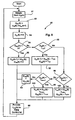
- Fig. 8 is a flow chart illustrating one method according to the present invention.
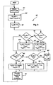
- Fig. 9 is a flow chart illustrating a second method according to the present invention.
- Fig 10 is a third flow chart illustrating a simplified method according to the present invention.
- Fig 11 is similar to Fig 1, albeit illustrating waveforms generated using the method of Fig 8;
- Fig. 12 is similar to Fig. 2, albeit illustrating spectrum corresponding to the waveforms of Fig. 11.
- a motor control system 50 including an inverter 52, a three phase motor 54, a pulse width modifier (PWM) controller 57, an overvoltage compensator 58, a comparator module 60, a modulating waveform generator 62 and a carrier signal generator 64.
- Inverter 52 receives positive and negative DC voltages provided on positive and negative DC buses and, as well known in the art, converts the DC voltage to three phase alternating voltage on three motor supply lines collectively identified by numeral 55.
- the supply lines 55 as their label implies, supply the AC voltages to separate phases of three phase motor 54.
- carrier signal generator 64 generates a saw tooth high frequency (e.g., 4-20 kHz) carrier signal C and provides the carrier signal to comparator module 60.
- the carrier signal C has a period Tc from signal peak to peak and has a half cycle period Tc/2 from each peak to a consecutively following valley.
- the carrier signal C actually comprises a counter value which counts from a high number value (e.g., 10,000) corresponding to a carrier signal peak to a zero value corresponding to a carrier signal valley and then back from the zero value up to the high number value at the next consecutive peak.
- a high number value e.g. 10,000
- the present invention will be described in the context of the aforementioned type of configuration where the carrier signal C corresponds to a counter value between zero and the high number value.
- Modulating waveform generator 62 generates three separate low frequency (e.g., 60 Hz) modulating waveforms (only one illustrated in Fig. 8) that may take any of several different forms well known in the art.
- the modulating waveform may be a pure sinusoidal waveform, a space-vector waveform, a third-harmonic waveform, a two-phase discontinuous waveform, etc. While three modulating waveforms are generated (one for each motor phase), in the interest of simplifying this explanation only one waveform and processing associated therewith will be described here. It should suffice to say that the processing described herein is repeated for each of the three waveforms.
- Waveform MW is provided to comparator module 60.
- waveform generator 62 generates a counter value corresponding to the waveform MW where the counter value changes in a fashion consistent with the type of modulating waveform. For example, where the modulating waveform is sinusoidal, the counter value changes in a sinusoidal fashion.
- comparator module 60 compares modulating waveform MW to carrier signal C and generates a trigger signal each time waveform MW and carrier signal C intersect. For example, in Fig 6, during labeled period T c , waveform MW intersects carrier signal C twice at times ⁇ 1 and ⁇ 2 and hence two trigger signals are generated during period T c . Where waveform MW and carrier signal C are counter values, comparator 60 simply compares the counter values to identify intersection points.
- waveform MW "intersects" carrier signal C moving from below to above count C (see ⁇ 1 in Fig. 6) the corresponding trigger signal will be referred to as an "on" trigger signal.
- the corresponding trigger signal will be referred to as an "off" trigger signal.
- the two on and off trigger signals or times that occur during each carrier period T c define a reference signal or firing pulse U rf that begins at the on trigger time ⁇ 1 , ends at the following off trigger time ⁇ 2 and remains high therebetween.
- label U rf will be used to refer to the reference pulse generally and also to the on and off times that occur during a carrier cycle.
- waveform MW may rise above the carrier signal peak T cp or drop below the carrier signal valley values.
- the reference signal Urf remains high during the entire period T c .
- the valley carrier value e.g., below count 0
- Comparator module 60 provides the reference signals U rf (and other signals corresponding to other system phases) to overvoltage compensator 58.
- Compensator 58 is programmed to compare reference signal U rf characteristics to a set of reference signal characteristics known to cause overvoltage conditions and to modify the reference signal U rf so that overvoltage is avoided.
- compensator 58 may or may not modify the on and off trigger times during each carrier cycle as a function of whether or not overvoltage will occur. While compensator 58 does not modify all reference signal pulses and, in fact, under certain operating conditions, does not modify any pulses, to simplify this explanation, the output of compensator 58 will be referred to as an altered reference signal U rfa .
- Altered signal U rfa is provided to PWM controller 57.
- Controller 57 uses the altered reference signals U rfa to generate firing pulses for inverter switches (not separately illustrated). Operation of PWM controllers 57 is well known in the art and therefore will not be explained herein detail.
- each altered reference signal U rfa is used to generate firing pulses for a separate one of three different inverter legs, a separate leg corresponding to each of the three motor phases.
- Each leg is controlled to alternately link the positive and negative DC buses to a corresponding motor supply line 55 thereby generating a series of high frequency voltage pulses on the line.
- the moving average of high frequency pulses generates the AC voltage waveform required to drive motor 54.
- controller 57 may be programmed to provide turn on delay and dead time compensation functionality, each of which is well known in the art.
- controller and inverter operation refer to U.S. Pat. No. 5,625,550 entitled “Apparatus Used With AC Motors For Compensating For Turn On Delay Errors” which issued on Apr. 29, 1997 and which is incorporated herein by reference for its teachings regarding controller and inverter operation.
- overvoltage compensator 58 includes a second pulse modifier 74, a comparator 72, a first pulse modifier 78 and an error identifier 76.
- Reference signal Urf from module 60 is received by second pulse modifier 74.
- an accumulated error U er corresponding to a previous carrier cycle is provided to pulse modifier 74 by error identifier 76.
- accumulated error U er corresponds to a rolling sum of all uncompensated modifications to previous reference signals (i.e., reference signals that occurred during previous carrier cycles). For example, where a reference signal U rf count corresponding to an on trigger time (see ⁇ 1 in Fig. 6) is modified by reducing the count by 100 to avoid overvoltage conditions, 100 is added to (i.e., accumulated) the accumulated error U er . Where the next trigger on time corresponding to the next carrier period is modified by reducing the count by 120 to avoid overvoltage conditions, 120 is added to the accumulated error U er and so on. Modifier 74 adds the accumulated error U er to the reference signal U rf thereby generating a composite reference signal U rfc Composite reference signal U rfc is provided to comparator 72.
- comparator 72 is also provided with four values used to identify overvoltage conditions under which different types of reference signal modifications are needed.
- the four values provided to comparator 72 include a zero value, a carrier signal duration value T c a maximum pulse time value T max and a minimum pulse time value T min .
- the maximum pulse time T max corresponds to the maximum pulse width for a reference signal U ref that can be generated without causing overvoltage conditions to occur.
- the minimum pulse time value T min corresponds to the minimum pulse width or duration that can be generated without causing overvoltage conditions to occur. Algorithms and systems for identifying the maximum and minimum pulse time values T max and T min , respectively, are well known in the art and therefore will not be described here in detail.
- Comparator 72 performs several steps to determine whether or not the composite reference signal U rfc provided by modifier 74 will cause an overvoltage condition to occur.
- An exemplary algorithm performed by comparator 72 is described below with respect to Fig. 8.
- Pulse modifier 78 alters the composite reference signals as a function of the results of the comparisons performed by comparator 72 and then provides altered reference signals to PWM controller 57.
- Modifier 78 also provides an indication to error identifier 76 indicating how the composite reference signal was altered to generate the altered signal. As indicated above identifier 76 accumulates the changes or "errors" so that those changes can be subsequently compensated.
- second pulse modifier 74 receives the most recently generated accumulated error count U er (k-1) from error identifier 76 and also receives an initial reference signal count U rf (k) from comparator module 60 and adds the two received signals to generate a composite reference signal U rfc (k).
- the modifier 74 sets the accumulated error count U er (k) equal to zero.
- comparator 72 compares the composite signal U rfc (k) to zero to determine whether or not the composite signal is less than zero. Where the composite signal is less than zero, control passes to block 88 where first pulse modifier 78 sets an altered reference signal U rfa (k) equal to zero. In addition, at block 88, error identifier 76 identifies the difference between the composite reference signal U rfc (k) and the altered reference U rfa (k) and sets the accumulated reference error signal U er (k-1) equal to the difference. In this case, because the altered reference signal U rfa (k) is zero, the difference amounts to the composite reference signal value U rfc (k).
- error identifier 76 determines the difference between the composite reference signal U rfc (k) and the peak carrier signal value T cp by subtracting the peak carrier signal value T cp from the composite signal U rfc (k) to identify the accumulated reference error signal U er (k-1).
- control again passes to block 95 where the adjusted reference signal U rfa (k) is provided to the PWM controller. After block 95 the cycle is repeated again.
- control passes to block 96.
- comparator 72 compares the composite reference signal U rfc (k) to the minimum pulse time T min . Where the composite signal U rfc (k) is less than the minimum pulse time value T min , control passes from block 96 to block 102.
- first pulse modifier 78 sets the adjusted reference signal U rfa (k) equal to the minimum pulse time value T min .
- error identifier 76 sets the accumulated error signal U er (k) equal to the difference between the composite reference signal U rf (k) and the adjusted reference signal U rfa (k). To this end, identifier 76 subtracts the minimum pulse time value T min from the composite signal U rfc (k) to generate the accumulated error signal U er (k). After block 102, control passes to block 95 and then on to block 81 where the cycle is repeated.
- error identifier 76 identifies the difference between the composite reference signal U rfc (k) and the adjusted reference U rfa (k) as the accumulated error signal U er (k). To this end, error identifier 76 subtracts the maximum pulse value T max from the composite signal U rfc (k) to generate the accumulated error signal U er (k). After block 100, control again passes to block 95 and thereafter up to block 81 where the cycle is repeated.
- Fig. 11 experimental results generated using the inventive algorithm of Fig. 8 with an IGBT inverter are illustrated. To generate the waveforms in Fig. 11, a 10 HP motor was operated at no load and at 55 Hz with a 630v bus, a 4 kHz carrier signal and with a 16 micro-second dwell time.
- Figure 12 illustrates voltage and phase currents spectrum corresponding to the waveforms in Fig. 11. Comparing Figs. 11 and 12 to Figs. 1 and 2 and also to Figs. 3 and 4, it should be appreciated that the new method with extended dwell time produces a far better quality waveform than previous solutions.
- decision block 86 and 90 may be swapped so that the composite reference signal U rfc (k) is first compared to the peak carrier signal value T cp and, thereafter, is compared to the zero value.
- decision blocks 96 and 98 may be swapped so that the comparison process is performed in a different sequence.
- Fig. 9 illustrates an alternate method 80' according to the present invention.
- decision and process blocks that are similar to the decision and process blocks illustrated in Fig. 8 are identified by similar numbers followed by a ""'.
- the functions corresponding to blocks in Fig. 9 are essentially identical to the functions described above with respect to the similarly labeled blocks in Fig 8, the only difference being the order in which the functions are performed. For this reason, the specific functions performed by each block in Fig. 9 will not be described again here in detail. With respect the different order, after block 84' in Fig.
- comparison of the composite reference signal U rfc (k) to the minimum and maximum pulse times T min and T max , respectively, is performed prior to comparison of the composite reference signal U rfc (k) to the zero value and/or the peak carrier signal value T cp .
- the adjusted reference signal U rfa (k) and the accumulated error signal U er (k) may be set at one of blocks 100' and 102', each one of those values may be reset at one of blocks 88' or 92' prior to providing the adjusted reference signal U rfa (k) to the PWM controller at block 95'.
- FIG. 10 yet one other simplified method 80" according to the present invention is illustrated.
- blocks that are similar to the block in Fig. 8 are identified by identical numbers followed a " " " and, similar blocks perform similar functions. Again, in the interest of simplifying this explanation, the operation of each of the blocks in Fig 10 will not be explained again herein detail.
- the process 80" is generally different than process described above with respect to Fig. 8 in that process 80" does not eliminate pulses but instead limits pulses to the maximum and minimum pulse times allowable. In this regard, process 80" does not include functions corresponding to blocks 86, 88, 90 or 92 as illustrated in Fig. 8 above.
- the composite reference signal U rfc (k) is compared to the minimum and maximum pulse times T max and T min , respectively.
- all of the altered reference signals U rfa (k) may be set equal to either a zero value or the peak carrier signal value T cp .
- a method of this type would include blocks 86, 88, 90 and 92 but would not include blocks 96, 98, 100 or 102.
- a method and apparatus are disclosed to be used with a motor controller generating firing pulses to control an inverter, the inverter providing exciting voltage to a motor corresponding to the firing pulses, the voltage having a maximum intended amplitude, the method for substantially eliminating exciting voltage overvoltage by modifying the firing pulses, the method comprising the steps of identifying characteristics of an initial firing pulse, comparing the initial pulse characteristics to an overvoltage characteristic set known to cause overvoltage, where the initial pulse characteristics match the overvoltage characteristic set, altering the initial firing pulse such that the altered firing pulse does not cause overvoltage, identifying an accumulated error corresponding to the altered firing pulse, modifying the firing pulse following the altered firing pulse as a function of the accumulated error to generate a composite firing pulse; and repeating the identifying, comparing, altering, identifying and modifying process with the composite firing pulse as the initial firing pulse.
Landscapes
- Engineering & Computer Science (AREA)
- Power Engineering (AREA)
- Inverter Devices (AREA)
- Control Of Ac Motors In General (AREA)
Applications Claiming Priority (2)
| Application Number | Priority Date | Filing Date | Title |
|---|---|---|---|
| US365268 | 2003-02-12 | ||
| US10/365,268 US6819070B2 (en) | 2003-02-12 | 2003-02-12 | Method and apparatus for controlling reflected voltage using a motor controller |
Publications (3)
| Publication Number | Publication Date |
|---|---|
| EP1447904A2 true EP1447904A2 (fr) | 2004-08-18 |
| EP1447904A3 EP1447904A3 (fr) | 2005-10-12 |
| EP1447904B1 EP1447904B1 (fr) | 2012-01-11 |
Family
ID=32681706
Family Applications (1)
| Application Number | Title | Priority Date | Filing Date |
|---|---|---|---|
| EP04002804A Expired - Lifetime EP1447904B1 (fr) | 2003-02-12 | 2004-02-09 | Méthode et appareil pour la suppression de surtensions dans un onduleur à modulation de largeur d'impulsion |
Country Status (2)
| Country | Link |
|---|---|
| US (1) | US6819070B2 (fr) |
| EP (1) | EP1447904B1 (fr) |
Cited By (1)
| Publication number | Priority date | Publication date | Assignee | Title |
|---|---|---|---|---|
| CN102291083A (zh) * | 2010-06-07 | 2011-12-21 | 洛克威尔自动控制技术股份有限公司 | 共模电压降低设备和用于基于电流源转换器的驱动器的方法 |
Families Citing this family (29)
| Publication number | Priority date | Publication date | Assignee | Title |
|---|---|---|---|---|
| US7145300B2 (en) * | 2003-05-05 | 2006-12-05 | International Rectifier Corporation | Multi-axis AC servo control system and method |
| JP4312760B2 (ja) * | 2003-08-25 | 2009-08-12 | 三菱電機株式会社 | 電力変換装置の制御装置 |
| JP4581574B2 (ja) * | 2004-09-08 | 2010-11-17 | 株式会社ジェイテクト | モータ制御装置及び電動パワーステアリング装置 |
| US20060066274A1 (en) * | 2004-09-30 | 2006-03-30 | Valeo Electrical Systems, Inc. | Overmodulation of electric motor in power steering system |
| US7106025B1 (en) * | 2005-02-28 | 2006-09-12 | Rockwell Automation Technologies, Inc. | Cancellation of dead time effects for reducing common mode voltages |
| US7286375B1 (en) * | 2007-01-23 | 2007-10-23 | Gm Global Technology Operations, Inc. | Dead-time compensation method for electric drives |
| US7738267B1 (en) * | 2009-01-07 | 2010-06-15 | Rockwell Automation Technologies, Inc. | Systems and methods for common-mode voltage reduction in AC drives |
| US7881081B1 (en) | 2010-04-16 | 2011-02-01 | Rockwell Automation Technologies, Inc. | Systems and methods for reducing AC drive common-mode currents |
| WO2011135696A1 (fr) * | 2010-04-28 | 2011-11-03 | 株式会社 日立製作所 | Dispositif de conversion de puissance |
| US8503207B2 (en) | 2010-09-29 | 2013-08-06 | Rockwell Automation Technologies, Inc. | Discontinuous pulse width drive modulation method and apparatus for reduction of common-mode voltage in power conversion systems |
| US8488345B2 (en) | 2010-12-01 | 2013-07-16 | Rockwell Automation Technologies, Inc. | Pulse width modulation control method and system for mitigating reflected wave effects in over-modulation region |
| US9353732B2 (en) * | 2010-12-23 | 2016-05-31 | Vestas Wind Systems A/S | Method of operating a wind turbine as well as a system suitable therefor |
| US9362839B2 (en) | 2011-02-09 | 2016-06-07 | Rockwell Automation Technologies, Inc. | Power converter with common mode voltage reduction |
| US8379417B2 (en) | 2011-07-06 | 2013-02-19 | Rockwell Automation Technologies, Inc. | Power converter and integrated DC choke therefor |
| JP5776496B2 (ja) * | 2011-10-31 | 2015-09-09 | 富士電機株式会社 | 電力変換装置 |
| DE102011118044A1 (de) * | 2011-11-09 | 2013-05-16 | Conti Temic Microelectronic Gmbh | Verfahren zur Steuerung eines Motors mittels Pulsweitenmodulation (PWM) |
| US9054599B2 (en) | 2012-03-15 | 2015-06-09 | Rockwell Automation Technologies, Inc. | Power converter and integrated DC choke therefor |
| US9425705B2 (en) | 2012-08-13 | 2016-08-23 | Rockwell Automation Technologies, Inc. | Method and apparatus for bypassing cascaded H-bridge (CHB) power cells and power sub cell for multilevel inverter |
| US9240731B2 (en) | 2013-03-18 | 2016-01-19 | Rockwell Automation Technologies, Inc. | Power cell bypass method and apparatus for multilevel inverter |
| US9520800B2 (en) | 2014-01-09 | 2016-12-13 | Rockwell Automation Technologies, Inc. | Multilevel converter systems and methods with reduced common mode voltage |
| US9325252B2 (en) | 2014-01-13 | 2016-04-26 | Rockwell Automation Technologies, Inc. | Multilevel converter systems and sinusoidal pulse width modulation methods |
| US9559541B2 (en) | 2015-01-15 | 2017-01-31 | Rockwell Automation Technologies, Inc. | Modular multilevel converter and charging circuit therefor |
| US9748862B2 (en) | 2015-05-13 | 2017-08-29 | Rockwell Automation Technologies, Inc. | Sparse matrix multilevel actively clamped power converter |
| US9812990B1 (en) | 2016-09-26 | 2017-11-07 | Rockwell Automation Technologies, Inc. | Spare on demand power cells for modular multilevel power converter |
| US11303224B2 (en) * | 2018-01-25 | 2022-04-12 | Kabushiki Kaisha Toyota Jidoshokki | Inverter device with high follow-up capability |
| US10158299B1 (en) | 2018-04-18 | 2018-12-18 | Rockwell Automation Technologies, Inc. | Common voltage reduction for active front end drives |
| DE102018121888A1 (de) * | 2018-09-07 | 2020-03-12 | Danfoss Power Electronics A/S | Verfahren zum Einstellen eines Wechselrichters, der über einen du/dt-Filter mit einem Elektromotor verbunden ist |
| US11211879B2 (en) | 2019-09-23 | 2021-12-28 | Rockwell Automation Technologies, Inc. | Capacitor size reduction and lifetime extension for cascaded H-bridge drives |
| US11342878B1 (en) | 2021-04-09 | 2022-05-24 | Rockwell Automation Technologies, Inc. | Regenerative medium voltage drive (Cascaded H Bridge) with reduced number of sensors |
Citations (1)
| Publication number | Priority date | Publication date | Assignee | Title |
|---|---|---|---|---|
| US5671130A (en) | 1996-08-23 | 1997-09-23 | Allen-Bradley Company, Inc. | Method and apparatus for controlling voltage reflections using a motor controller |
Family Cites Families (12)
| Publication number | Priority date | Publication date | Assignee | Title |
|---|---|---|---|---|
| EP0105215B1 (fr) * | 1982-09-07 | 1987-03-04 | Hitachi, Ltd. | Appareil de contrôle pour moteurs à courant alternatif |
| US4904919A (en) * | 1988-06-21 | 1990-02-27 | Allen-Bradley Company, Inc. | Dual mode control of a PWM motor drive for current limiting |
| US5625550A (en) | 1994-09-27 | 1997-04-29 | Allen-Bradley Company, Inc. | Apparatus used with AC motors for compensating for turn on delay errors |
| US5610806A (en) * | 1995-06-19 | 1997-03-11 | Allen-Bradley Company, Inc. | Pulse width modulation method for driving three phase power inverter/converter switches with balanced discontinuous phase commands |
| US5736825A (en) | 1996-06-25 | 1998-04-07 | Allen-Bradley Company, Inc. | Method and apparatus for linearizing pulse width modulation by modifying command voltges |
| US5706186A (en) | 1996-09-23 | 1998-01-06 | Allen-Bradley Company, Inc. | Hybrid pulse width modulation method and apparatus |
| US5811949A (en) | 1997-09-25 | 1998-09-22 | Allen Bradley Company, Llc | Turn-on delay compensator for motor control |
| US5912813A (en) | 1997-10-01 | 1999-06-15 | Allen-Bradley Company, Llc | Method and apparatus for controlling reflected voltage using a motor controller |
| US6014497A (en) | 1997-10-01 | 2000-01-11 | Allen-Bradley Company, Llc | Method and apparatus for determining a critical dwell time for use in motor controls |
| US5990658A (en) | 1998-01-22 | 1999-11-23 | Allen-Bradley Company, Llc | Apparatus for controlling reflected voltage on motor supply lines |
| US6023417A (en) | 1998-02-20 | 2000-02-08 | Allen-Bradley Company, Llc | Generalized discontinuous pulse width modulator |
| US6541933B1 (en) * | 2001-11-20 | 2003-04-01 | Rockwell Automation Technologies, Inc. | Angle control of modulating wave to reduce reflected wave overvoltage transients |
-
2003
- 2003-02-12 US US10/365,268 patent/US6819070B2/en not_active Expired - Lifetime
-
2004
- 2004-02-09 EP EP04002804A patent/EP1447904B1/fr not_active Expired - Lifetime
Patent Citations (1)
| Publication number | Priority date | Publication date | Assignee | Title |
|---|---|---|---|---|
| US5671130A (en) | 1996-08-23 | 1997-09-23 | Allen-Bradley Company, Inc. | Method and apparatus for controlling voltage reflections using a motor controller |
Non-Patent Citations (1)
| Title |
|---|
| KERKMAN R J ET AL.: "PWM inverters and their influence on motor overvoltage", APEC '97, CONFERENCE PROCEEDINGS, vol. 1, 23 February 1997 (1997-02-23), pages 103 - 113, XP010215807, DOI: doi:10.1109/APEC.1997.581440 |
Cited By (2)
| Publication number | Priority date | Publication date | Assignee | Title |
|---|---|---|---|---|
| CN102291083A (zh) * | 2010-06-07 | 2011-12-21 | 洛克威尔自动控制技术股份有限公司 | 共模电压降低设备和用于基于电流源转换器的驱动器的方法 |
| CN102291083B (zh) * | 2010-06-07 | 2014-04-23 | 洛克威尔自动控制技术股份有限公司 | 共模电压降低设备和用于基于电流源转换器的驱动器的方法 |
Also Published As
| Publication number | Publication date |
|---|---|
| EP1447904A3 (fr) | 2005-10-12 |
| US20040160207A1 (en) | 2004-08-19 |
| US6819070B2 (en) | 2004-11-16 |
| EP1447904B1 (fr) | 2012-01-11 |
Similar Documents
| Publication | Publication Date | Title |
|---|---|---|
| US6819070B2 (en) | Method and apparatus for controlling reflected voltage using a motor controller | |
| US6541933B1 (en) | Angle control of modulating wave to reduce reflected wave overvoltage transients | |
| EP2475088B1 (fr) | Procédé de contrôle de modulation de largeur d'impulsion et système pour atténuer les effets d'onde reflétée dans une région de surmodulation | |
| US7106025B1 (en) | Cancellation of dead time effects for reducing common mode voltages | |
| EP2395652B1 (fr) | Systèmes et procédés pour réduire les courants en mode commun d'un entraînement CA | |
| US6617821B2 (en) | Method and apparatus for compensating for device dynamics by adjusting inverter carrier frequency | |
| US8030874B2 (en) | Power converting apparatus | |
| EP2393197A2 (fr) | Appareil de réduction de tension en mode commun et procédé pour entraînement basé sur un convertisseur de source de courant | |
| CN111919375B (zh) | 功率转换装置 | |
| US5610806A (en) | Pulse width modulation method for driving three phase power inverter/converter switches with balanced discontinuous phase commands | |
| EP2214301A1 (fr) | Systèmes de conversion de puissance et procédés pour le contrôle de la distorsion harmonique | |
| US5671130A (en) | Method and apparatus for controlling voltage reflections using a motor controller | |
| US6297613B1 (en) | Control of line harmonics | |
| JPH0851790A (ja) | 誘導性負荷用制御回路 | |
| US6246209B1 (en) | Control device for alternating current motor | |
| US5990658A (en) | Apparatus for controlling reflected voltage on motor supply lines | |
| Patel et al. | Pulse-based dead-time compensation method for self-balancing space vector pulse width-modulated scheme used in a three-level inverter-fed induction motor drive | |
| JP2007252191A (ja) | 低周波数においてacモータ・トルク出力を増大させる方法及び装置 | |
| Materu et al. | Steady-state analysis of the variable-speed switched-reluctance motor drive | |
| Kim et al. | An analytical design strategy and implementation of a dv/dt filter for WBG devices based high speed machine drives | |
| JP2020048381A (ja) | モータ制御装置、モータシステム及びインバータ制御方法 | |
| JP5428744B2 (ja) | 電力変換装置の制御方法 | |
| Rahman et al. | A study of THD minimization of three phase inverter using modified THPWM | |
| EP4304072A1 (fr) | Dispositif de commande d'onduleur | |
| US20250233526A1 (en) | Dc-link voltage ramp-up |
Legal Events
| Date | Code | Title | Description |
|---|---|---|---|
| PUAI | Public reference made under article 153(3) epc to a published international application that has entered the european phase |
Free format text: ORIGINAL CODE: 0009012 |
|
| AK | Designated contracting states |
Kind code of ref document: A2 Designated state(s): AT BE BG CH CY CZ DE DK EE ES FI FR GB GR HU IE IT LI LU MC NL PT RO SE SI SK TR |
|
| AX | Request for extension of the european patent |
Extension state: AL LT LV MK |
|
| PUAL | Search report despatched |
Free format text: ORIGINAL CODE: 0009013 |
|
| AK | Designated contracting states |
Kind code of ref document: A3 Designated state(s): AT BE BG CH CY CZ DE DK EE ES FI FR GB GR HU IE IT LI LU MC NL PT RO SE SI SK TR |
|
| AX | Request for extension of the european patent |
Extension state: AL LT LV MK |
|
| 17P | Request for examination filed |
Effective date: 20060210 |
|
| AKX | Designation fees paid |
Designated state(s): CH DE FR GB IT LI |
|
| 17Q | First examination report despatched |
Effective date: 20091109 |
|
| RIC1 | Information provided on ipc code assigned before grant |
Ipc: H02P 27/08 20060101ALI20110412BHEP Ipc: H02M 7/5387 20070101AFI20110412BHEP Ipc: H02M 1/32 20070101ALI20110412BHEP |
|
| GRAP | Despatch of communication of intention to grant a patent |
Free format text: ORIGINAL CODE: EPIDOSNIGR1 |
|
| GRAS | Grant fee paid |
Free format text: ORIGINAL CODE: EPIDOSNIGR3 |
|
| GRAA | (expected) grant |
Free format text: ORIGINAL CODE: 0009210 |
|
| AK | Designated contracting states |
Kind code of ref document: B1 Designated state(s): CH DE FR GB IT LI |
|
| REG | Reference to a national code |
Ref country code: GB Ref legal event code: FG4D |
|
| REG | Reference to a national code |
Ref country code: CH Ref legal event code: EP |
|
| REG | Reference to a national code |
Ref country code: DE Ref legal event code: R096 Ref document number: 602004036042 Country of ref document: DE Effective date: 20120308 |
|
| PLBE | No opposition filed within time limit |
Free format text: ORIGINAL CODE: 0009261 |
|
| STAA | Information on the status of an ep patent application or granted ep patent |
Free format text: STATUS: NO OPPOSITION FILED WITHIN TIME LIMIT |
|
| PG25 | Lapsed in a contracting state [announced via postgrant information from national office to epo] |
Ref country code: IT Free format text: LAPSE BECAUSE OF FAILURE TO SUBMIT A TRANSLATION OF THE DESCRIPTION OR TO PAY THE FEE WITHIN THE PRESCRIBED TIME-LIMIT Effective date: 20120111 |
|
| 26N | No opposition filed |
Effective date: 20121012 |
|
| REG | Reference to a national code |
Ref country code: DE Ref legal event code: R097 Ref document number: 602004036042 Country of ref document: DE Effective date: 20121012 |
|
| REG | Reference to a national code |
Ref country code: FR Ref legal event code: PLFP Year of fee payment: 13 |
|
| REG | Reference to a national code |
Ref country code: FR Ref legal event code: PLFP Year of fee payment: 14 |
|
| REG | Reference to a national code |
Ref country code: FR Ref legal event code: PLFP Year of fee payment: 15 |
|
| PGFP | Annual fee paid to national office [announced via postgrant information from national office to epo] |
Ref country code: FR Payment date: 20210120 Year of fee payment: 18 Ref country code: CH Payment date: 20210120 Year of fee payment: 18 |
|
| PGFP | Annual fee paid to national office [announced via postgrant information from national office to epo] |
Ref country code: DE Payment date: 20210120 Year of fee payment: 18 Ref country code: GB Payment date: 20210120 Year of fee payment: 18 |
|
| REG | Reference to a national code |
Ref country code: DE Ref legal event code: R119 Ref document number: 602004036042 Country of ref document: DE |
|
| REG | Reference to a national code |
Ref country code: CH Ref legal event code: PL |
|
| GBPC | Gb: european patent ceased through non-payment of renewal fee |
Effective date: 20220209 |
|
| PG25 | Lapsed in a contracting state [announced via postgrant information from national office to epo] |
Ref country code: FR Free format text: LAPSE BECAUSE OF NON-PAYMENT OF DUE FEES Effective date: 20220228 |
|
| PG25 | Lapsed in a contracting state [announced via postgrant information from national office to epo] |
Ref country code: LI Free format text: LAPSE BECAUSE OF NON-PAYMENT OF DUE FEES Effective date: 20220228 Ref country code: GB Free format text: LAPSE BECAUSE OF NON-PAYMENT OF DUE FEES Effective date: 20220209 Ref country code: DE Free format text: LAPSE BECAUSE OF NON-PAYMENT OF DUE FEES Effective date: 20220901 Ref country code: CH Free format text: LAPSE BECAUSE OF NON-PAYMENT OF DUE FEES Effective date: 20220228 |