EP1449810B1 - Verfahren zur Herstellung eines mikroelektromechanischen Systems mit Lötkugeln - Google Patents
Verfahren zur Herstellung eines mikroelektromechanischen Systems mit Lötkugeln Download PDFInfo
- Publication number
- EP1449810B1 EP1449810B1 EP04251014A EP04251014A EP1449810B1 EP 1449810 B1 EP1449810 B1 EP 1449810B1 EP 04251014 A EP04251014 A EP 04251014A EP 04251014 A EP04251014 A EP 04251014A EP 1449810 B1 EP1449810 B1 EP 1449810B1
- Authority
- EP
- European Patent Office
- Prior art keywords
- alloy
- micro electro
- glass substrate
- via hole
- layer
- Prior art date
- Legal status (The legal status is an assumption and is not a legal conclusion. Google has not performed a legal analysis and makes no representation as to the accuracy of the status listed.)
- Expired - Lifetime
Links
Images


Classifications
-
- B—PERFORMING OPERATIONS; TRANSPORTING
- B81—MICROSTRUCTURAL TECHNOLOGY
- B81B—MICROSTRUCTURAL DEVICES OR SYSTEMS, e.g. MICROMECHANICAL DEVICES
- B81B7/00—Microstructural systems ; Auxiliary parts of microstructural devices or systems
- B81B7/0006—Interconnects
-
- H—ELECTRICITY
- H10—SEMICONDUCTOR DEVICES; ELECTRIC SOLID-STATE DEVICES NOT OTHERWISE PROVIDED FOR
- H10W—GENERIC PACKAGES, INTERCONNECTIONS, CONNECTORS OR OTHER CONSTRUCTIONAL DETAILS OF DEVICES COVERED BY CLASS H10
- H10W72/00—Interconnections or connectors in packages
- H10W72/071—Connecting or disconnecting
Definitions
- the present invention relates to a method for manufacturing micro electro-mechanical systems using solder balls. More particularly, the present invention relates to a method for manufacturing micro electro-mechanical systems that achieves efficient electrical connection between an internal structure and external electronic parts, and that protects the internal structure by preventing penetration of external air into a vacuum chamber during manufacture of wafer level packaging elements such as an angular velocity sensor, an acceleration sensor, a gyroscope sensor or a pressure sensor.
- Electronic parts of silicon micro-mechanical technology generally include a silicon substrate and two glass substrates bonded onto upper and lower surfaces of the silicon substrate.
- a structure for detecting angular velocity is formed on the silicon substrate, and the structure and silicon substrate are sealed by the two glass substrates.
- a method is known in the prior art for mounting micro electronic parts onto a surface of a circuit board using such technology.
- a method of manufacturing a micro electronic part has been used in which a via hole penetrates through an upper glass substrate, electrically connecting a structure formed on a semiconductor substrate with an external circuit board, so that electrical signals can be irradiated from the structure through the via hole.
- a conductive material is filled in the via hole enabling electrical connection between the external circuit board and the structure therethrough.
- the via hole may be formed to have a larger diameter because more air bubbles are usually generated in via holes of a smaller diameter.
- sizes of a corresponding part and a mounting surface also need to be increased.
- Another problem in the conventional method occurs because the conductive material filling the via hole differs from the glass substrate in thermal expansion coefficient. Therefore, a crack may be formed in the glass substrate when the electronic parts go through a thermal change.
- a conductive film instead of a conductive material may be provided on an inner wall of the via hole.
- the via hole is formed in the glass substrate by sand blasting, pieces of broken glass may be generated on the surface of the glass substrate and be bonded to the silicon substrate. Accordingly, when the glass substrate is bonded to the surface of the silicon substrate, a step-shaped portion may be formed due to the presence of the glass pieces between the silicon substrate and the via hole. As a result, connection of the conductive film may be hindered by the step-shaped portion causing a decrease in yield.
- FIG. 1 illustrates a main component of the micro electronic part formed by the method, including a silicon substrate 10, a glass substrate 20, a via hole 30 formed through the glass substrate 20, a vacuum chamber 40, micro electronic structure 50 and a micro electronic part having a conductive film.
- the conductive film is provided inside the via hole 30.
- An internal wall of the via hole 30 connects the glass substrate 20 to the silicon substrate 10. Therefore, disconnection due to glass pieces between the glass substrate 20 and the silicon substrate 10 may be avoided, and the structure can be electrically connected to the outside through the conductive film and a signal output portion.
- a soldering bump 60 is provided on a surface of the glass substrate as a part of the conductive film. By bonding the soldering bump 60 to an anodic pad on an external circuit board, the structure can be electrically connected with external devices.
- the conductive film is formed in the via hole by sputtering at a high vacuum of less than 10 -7 Torr using vapor depositing equipment, which my cause damage to an element. Accordingly, if the etching process requires more than several microns of vapor deposition for insulation between neighboring electrodes, problems may arise. Also, it is difficult to form fine pitches, and the elements may be damaged.
- forming a bump is difficult because a separate under bump metalization is required. If silk screen or metal plating is used for the under bump metalization, the conductive film may be damaged or contaminated.
- EP 1,203,748 discloses a micro device having a beam-like structure including a cantilever. An electrically conductive film is formed under the cantilever and protects a recess beneath the cantilever during etching.
- US 6,207,548 discloses a method for fabricating a chip scale package which uses bond pads.
- a method for manufacturing micro electro-mechanical systems including (a) forming an insulation layer on an upper surface of a semiconductor substrate and patterning the insulation layer, (b) forming a structure layer on an upper surface of the patterned insulation layer and etching the structure layer, (c) forming an under bump metal on a predetermined position of an upper surface of the structure layer, (d) forming a via hole in a glass substrate corresponding to the position of the under bump metal of the structure layer and in a shape such that the via hole is larger in diameter at an upper surface of the glass substrate than at a lower surface of the glass substrate, wherein the glass substrate is bonded to the upper surface of the structure layer and creates a vacuum chamber that protects a structure of the structure layer; and (e) arranging a solder ball in the via hole and bonding the solder ball to the under bump metal by melting the solder ball.
- the method of the invention is for manufacturing a micro electro-mechanical system having a small chip, in which a solder ball is arranged on a glass substrate where a via hole is formed to be electrically connected to a semiconductor substrate and an external circuit board, and which is capable of preventing penetration of air through the via hole.
- the structure layer is preferably formed using an inductively coupled plasma-reaction ion etching (ICP-RIE).
- ICP-RIE inductively coupled plasma-reaction ion etching
- the via hole is preferably formed using one of sand blasting, laser ablation and wet etching.
- the glass substrate is preferably bonded to the upper surface of the structure layer using either anodic bonding or soldering.
- (d) may further include removing an oxidation layer that is bonded onto the upper surface of the structure layer. Removing the oxidation layer may be performed by printing a flux or by melting under an inert gas atmosphere without the flux.
- the semiconductor substrate is preferably a silicon substrate.
- the insulation layer is preferably formed of one selected from the group consisting of Cr/Au alloy, Ti/Au alloy and Cr/Ni/Au alloy.
- the under bump metal is preferably formed of one selected from the group consisting of Cr/Au alloy, Ti/Au alloy, Cr/Ni/Au alloy and Cu/Ni/Au alloy.
- the solder ball is preferably formed of one selected from the group consisting of Sn/Pb alloy, In/Sn alloy, Au/Sn alloy, Ag/Cu alloy, In/Ag alloy, In/Bi alloy, Sn/Bi alloy, Sn/Cu alloy, Ag/Sn alloy, Sn/Ag/Cu alloy, Sn/Ag/Cu/Bi alloy, Sn/Ag/Bi alloy and Sn/Zn alloy.
- a method for manufacturing micro electro-mechanical systems including (a) forming an insulation layer on an upper surface of a semiconductor substrate and patterning the insulation layer, (b) forming a structure layer on an upper surface of the patterned insulation layer and etching the structure layer, (c) forming a via hole in a predetermined position of a glass substrate and in a shape such that the via hole is larger in diameter at an upper portion of the glass substrate than at a lower portion of the glass substrate, wherein the glass substrate is bonded to an upper surface of the structure layer and creates a vacuum chamber that protects a structure of the structure layer, (d) forming an under bump metal in a bottom of the via hole and forming a via side metal on an inner wall of the via hole, and (e) disposing a solder ball in the via hole and bonding the solder ball with the under bump metal and the via side metal by melting the solder ball.
- the structure layer is preferably formed using an inductively coupled plasma-reaction ion etching (ICP-RIE).
- ICP-RIE inductively coupled plasma-reaction ion etching
- the via hole is preferably formed using one of sand blasting, laser ablation and wet etching.
- the glass substrate is preferably bonded to the upper surface of the structure layer using either anodic bonding or soldering.
- (d) may further include removing an oxidation layer that is bonded onto the upper surface of the structure layer. Removing the oxidation layer may be performed by printing a flux or by melting under an inert gas atmosphere without the flux.
- the semiconductor substrate is preferably a silicon substrate.
- the insulation layer is preferably formed of one selected from the group consisting of Cr/Au alloy, Ti/Au alloy, and Cr/Ni/Au alloy.
- the under bump metal and the via side metal are preferably formed of one selected from the group consisting of Cr/Au alloy, Ti/Au alloy, Cr/Ni/Au alloy and Cu/Ni/Au alloy.
- the solder ball is preferably formed of one selected from the group consisting of Sn/Pb alloy, In/Sn alloy, Au/Sn alloy, Ag/Cu alloy, In/Ag alloy, In/Bi alloy, Sn/Bi alloy, Sn/Cu alloy, Ag/Sn alloy, Sn/Ag/Cu alloy, Sn/Ag/Cu/Bi alloy, Sn/Ag/Bi alloy and Sn/Zn alloy.
- FIG. 2 illustrates a micro electro-mechanical system fabricated according to a preferred embodiment of the present invention.
- the micro electro-mechanical system includes a semiconductor substrate 100, an insulation layer 200 formed on an upper surface of the semiconductor substrate 100, a structure layer 300 formed on an upper surface of the insulation layer 200, under bump metals 500a formed in predetermined positions in an upper surface of the structure layer 300, and a glass substrate 400 defining a vacuum chamber 401 that protects a structure on the structure layer 300 and having via holes 600 formed therein corresponding to positions of the under bump metals 500a.
- Solder balls 700 are disposed inside the via holes 600 and are joined with the under bump metals 500a by melting. Accordingly, the via holes 600, having step-shaped walls 601, are closed by the solder balls 70.
- FIG. 3 illustrates the micro electro-mechanical system of FIG. 2, but having a solder paste 900 disposed inside the via holes 500a rather than the solder balls 700 as illustrated in FIG. 2.
- solder paste 900 By the presence of the solder paste 900, the via holes 600 with the step-shaped wall 601 are closed.
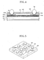
- FIG. 4 illustrates a micro electro-mechanical system fabricated according to another preferred embodiment of the present invention.
- the micro electro-mechanical system includes a semiconductor substrate 100, an insulation layer 200 formed on an upper surface of the semiconductor substrate 100, a structure layer 300 formed on an upper surface of the insulation layer 200, under bump metals 500a formed in predetermined positions of an upper surface of the structure layer 300, and a glass substrate 400 defining a vacuum chamber 401 that protects a structure formed on the structure layer 300 and having via holes 600 formed therein corresponding to positions of the under bump metals 500a.
- Via side metals 500b are formed in inner walls of the via holes 600, and the solder balls 700 are disposed in the via holes 600 and joined with the under bump metals 500a and the via side metals 500b through melting. Accordingly, the via holes 600, having step-shaped walls 601, are closed by the solder balls 70.
- a silicon substrate is preferable for the semiconductor substrate 100, and the insulation layer 200 is preferably formed of one selected from the group consisting of Cr/Au alloy, Ti/Au alloy and Cr/Ni/Au alloy.
- Both the under bump metals 500a and the via side metals 500b are preferably formed of one selected from the group consisting of Cr/Au alloy, Ti/Au alloy, Cr/Ni/Au alloy, and Cu/Ni/Au alloy.
- the solder balls 700 are preferably formed of one selected from the group consisting of Sn/Pb alloy, Au/Sn alloy, Ag/Cu alloy, In/Ag alloy, In/Bi alloy, Sn/Bi alloy, Sn/Cu alloy, Ag/Sn alloy, Sn/Ag/Cu alloy, Sn/Ag/Cu/Bi alloy, Sn/Ag/Bi alloy, and Sn/Zn alloy.
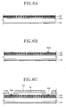
- FIG. 5 illustrates a micro electro-mechanical system fabricated according to a preferred embodiment of the present invention being diced.
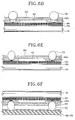
- FIGS. 6A to 6F illustrate in detail a method for manufacturing micro electro-mechanical systems according to preferred embodiments of the present invention.
- the insulation layer 200 which may be a sacrificial layer, is formed on the silicon substrate that is provided as the semiconductor substrate 100.
- the structure layer 300 is formed on an upper surface of the insulation layer 200, and an etching process is performed.
- structures of wafer level packaging such as a gyroscope sensor or an acceleration sensor are formed using inductively coupled plasma-reaction ion etching (ICP-RIE).
- a layer (not shown) of Cr/Au alloy, Ti/Au alloy, Cr/Ni/Au alloy or Cu/Ni/Au alloy is formed on an upper surface of the structure layer 300 by vapor deposition, and the layer is patterned to form the under bump metals 500a on the structure layer 300 in predetermined locations.
- anodic bonding is achieved by connecting an electrode to a glass substrate having a silicon or other oxidizable layer coated thereon, applying a voltage of more than several hundred volts to the glass substrate, and subsequently forming an oxidation layer on a boundary of the glass substrate and the that to which it is being bonded.
- the structure layer 300 and the glass substrate 400 may be joined by soldering rather than anodic bonding.
- soldering is a process using adhesives, in which solder is vapor-deposited, plated or printed and then heated to bond items together. In a case of melting a solder ball, flux is printed or dispensed to remove the oxidation layer. Melting without flux under an inert gas atmosphere is also possible.
- the glass substrate 400 is formed to have a space therein such that a vacuum 401 is created to protect the structure formed on the structure layer 300.
- the via holes 600 are formed in the glass substrate 400 by sand blasting.
- the via holes 600 are formed to have an inverse triangle shape, which is larger in diameter at an upper portion of the glass substrate 400 than at a lower portion thereof, which is a contact area between the glass substrate 400 and the structure layer 300.
- the solder balls 700 are disposed in the via holes 600 using solder ball placement equipment.
- the inverse triangle shape of the via holes 600 allows easy positioning of the solder balls 700 therein.
- the solder balls 700 in the via holes 600 are contacted with the under bump metals 500a either by laser or by applying a predetermined pressure thereto.
- the solder balls 700 and the under bump metals 500a are joined with each other using thermal chemical binding by heating the micro electro-mechanical system under an inert gas atmosphere at a temperature above a melting point of the solder. Because the solder balls 700 are melted in the contact holes 600 to be bonded with the under bump metals 500a, it is not necessary to form a conductive film in the contact holes 600 to provide an electrical connection between the micro electro-mechanical system and an external substrate. Therefore, damage to the substrate due to sputtering is prevented.
- FIG. 5 shows the micro electro-mechanical system according to a preferred embodiment of the present invention after being diced.
- the micro electro-mechanical system fabricated according to the present invention can be bonded to an external printed circuit board (PCB) 800 by a flip-chip method. That is, the micro electro-mechanical system is flipped and the solder balls 700 are placed at predetermined positions on the external PCB 800 and the solder balls 700 are joined to the external PCB 800 by heating the solder balls 700 at a temperature above the melting point of the solder.
- PCB printed circuit board
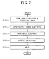
- FIGS. 7 and 8 are flowcharts illustrating a method for manufacturing micro electro-mechanical systems according to preferred embodiments of the present invention.
- step S110 an insulation layer and a structure layer are formed (step S110).
- step S210 under bump metals are deposited on the upper surface of the structure layer by vapor deposition (step S210), and a glass substrate is bonded to the structure layer (step S310).
- Solder balls are positioned in via holes formed in the glass substrate (step S410), and then melted (step S510). As a result, a micro electro-mechanical system according to a preferred embodiment of the present invention is fabricated.
- step S610 an insulation layer (or sacrificial layer) and a structure layer are formed (step S610), and a glass substrate is bonded to an upper surface of the structure layer (step S710).
- step S810 via side metals are vapor-deposited on inner walls of via holes of the glass substrate and under bump metals are vapor deposited in bottoms of the via holes (step S810).
- Solder balls are disposed in the via holes (step S910) and melted (step S1010), and as a result, a micro electro-mechanical system according to another preferred embodiment of the present invention is fabricated.
- an insulation layer is formed on a silicon substrate, which is a semiconductor substrate, and then a structure layer is formed thereon.
- a structure for wafer level packaging such as a gyroscope sensor or an acceleration sensor is formed on the structure layer by an inductively coupled plasma-reaction ion etching (ICP-RIE) process.
- ICP-RIE inductively coupled plasma-reaction ion etching
- a glass substrate is bonded onto the structure layer by anodic bonding.
- Soldering instead of anodic bonding, may be used to bond the structure layer with the glass substrate.
- under bump metals are formed, and via side metals are formed on inner walls of the via holes.
- the under bump metals may be formed of one selected from the group consisting of Cr/Au alloy, Ti/Au alloy, and Cr/Ni/Au alloy through vapor-deposition and patterning
- the via side metals may be formed of one selected from the group consisting of Cr/Au alloy, Ti/Au alloy, Cr/Ni/Au alloy and Cu/Ni/Au alloy also through vapor-deposition and patterning.
- flux is printed or dispensed in order to remove the oxidation layer. Melting is also possible under an inert gas atmosphere such as Ar or N 2 without flux.
- Solder balls are positioned in the via holes using solder ball placement equipment.
- the via holes are shaped to the shape of an inverse triangle, which is larger in diameter at an upper portion of the glass substrate than at the plane where the glass substrate meets the structure layer. Due to the inverse triangular shape of the via holes, the solder balls can be easily positioned in the via holes.
- the solder balls are contacted to the under bump metals and the via side metals either using a laser or by applying a predetermined pressure.
- the solder balls are joined with the under bump metals and the via side metals through thermal chemical bonding by heating the micro electro-mechanical system at a temperature above a melting point of the solder balls under an inert gas atmosphere. Because the solder balls are contacted with the under bump metals and the via side metals as described above, there is no need to form a conductive film in the via holes to electrically connect the micro electro-mechanical system with an external substrate. Accordingly, the present invention can solve the problem of the conventional case in which pieces of broken glass are produced during the formation of the via holes through sand blasting, and the broken glass pieces cause step-shaped portions in inner walls of the via holes between the glass substrate and the silicon substrate contacted with the glass substrate. Furthermore, because the solder balls are joined with the under bump metals and the via side metals, leakage through an empty space below the solder balls and step-shaped portions in the sides of the via holes can be prevented.
- FIG. 5 illustrates a micro electro-mechanical system according to a preferred embodiment of the present invention after the dicing process.
- the micro electro-mechanical system fabricated according to the present invention can be bonded to an external PCB by a flip-chip method. That is, the micro electro-mechanical system is flipped so that solder balls in via holes are aligned with predetermined locations on the external PCB. Then, by heating at a temperature above a melting point of the solder balls, the solder balls are bonded to the external PCB.
- the problem of having pieces of broken glass produced at the lower end of the glass substrate during sand blasting for formation of the via holes, formation of step-shaped portions due to the glass pieces, and subsequent electrical disconnection from the external substrate due to the step-shaped portions, can be prevented. Furthermore, in the micro electro-mechanical systems according to the present invention, because the under bump metals and the via side metals are joined with the solder balls by melting and are electrically connected with each other, there is no need for an additional conductive film in the via holes, and accordingly, damage to the system by sputtering of vapor-deposition equipment under a high vacuum below 10 -7 Torr can be prevented.
- solder balls in the via holes is made easier because of the inverted triangular shape of the via holes, and joining with the external PCB also becomes easier because the solder balls forming bumps on the glass substrate make alignment of the PCB with the glass substrate easier.
- solder balls are joined with under bump metals and/or via side metals and thus allow electrical connection of electrical signals inside the system with external electrical parts. As a result, a defective electrical connection may be prevented, and realization of a flip-chip is enabled. Accordingly, a compact-sized product may be produced.
- wire bonding can be omitted and automatic arrangement of the solder balls in the via holes of the glass substrate is enabled. Because automation is enabled, benefits such as an increase in yield and a decrease in manufacturing costs may be obtained. Also, leakage through step-shaped portions in the via holes of the glass substrate may be prevented by the presence of the solder balls, and performance may therefore be increased.
- the system can be arranged with respect to an external PCB in the form of a flip-chip, a connecting process becomes simplified, and benefits such as high integration and compactness may be obtained. As a result, a number of signal input/output terminals with respect to a unit area may be increased and reduced in size. Finally, since there is no need for a separate die attachment, accuracy in the assembling arrangement may be improved.
Landscapes
- Engineering & Computer Science (AREA)
- Computer Hardware Design (AREA)
- Microelectronics & Electronic Packaging (AREA)
- Micromachines (AREA)
- Wire Bonding (AREA)
Claims (12)
- Verfahren zur Herstellung mikroelektromechanischer Systeme, das Folgendes umfasst:(a) Ausbilden einer Isolationsschicht (200) auf einer Oberseite eines Halbleitersubstrats (100) und Strukturieren der Isolationsschicht;(b) Ausbilden einer Strukturschicht (300) auf einer Oberseite der strukturierten Isolationsschicht (200) und Ätzen der Strukturschicht (300);(c) Ausbilden eines Kontaktlochs (600) in einem Glassubstrat (400) und in einer solchen Gestalt, dass das Kontaktloch einen größeren Durchmesser auf einer Oberseite des Glassubstrats aufweist als auf einer Unterseite des Glassubstrats(400), wobei das Glassubstrat (400) zum Bonden an die Oberseite der Strukturschicht (300) vorgesehen ist, um eine Vakuumkammer (401) zu bilden, die eine Struktur der Strukturschicht (300) schützt, wobei ein Kontakthügel-Untermetall (500a) an einer Position, die dem Kontaktloch (600) entspricht, ausgebildet ist; und(d) Anordnen einer Lötperle (700) in dem Kontaktloch (600) und Bonden der Lötperle (700) an das Kontakthügel-Untermetall (500a) durch Schmelzen der Lötperle (700).
- Verfahren zur Herstellung mikroelektromechanischer Systeme nach Anspruch 1, wobei das Kontakthügel-Untermetall (500a) an einer vorgegebenen Position einer Oberseite der Strukturschicht (300) ausgebildet wird und das Glassubstrat (400) an die Oberseite der Strukturschicht (300) gebondet wird, nachdem die Kontakthügel-Unterschicht ausgebildet wurde.
- Verfahren zur Herstellung mikroelektromechanischer Systeme nach Anspruch 1, wobei das Kontakthügel-Untermetall (500a) an einem Boden des Kontaktlochs (600) ausgebildet wird und ein Kontaktlochseitenmetall (500b) an einer Innenwand des Kontaktlochs (600) bildet, wobei das Glassubstrat (400) an die Oberseite der Strukturschicht (300) gebondet wird, bevor die Kontakthügel-Unterschicht ausgebildet wird, und wobei die Lötperle (700) an das Kontakthügel-Untermetall (500a) und an das Kontaktlochseitenmetall (500b) gebondet wird.
- Verfahren zur Herstellung mikroelektromechanischer Systeme nach einem der vorangehenden Ansprüche, wobei in (b) die Strukturschicht (300) mittels reaktivem Ionenätzen mit induktiv gekoppeltem Plasma (ICP-RIE) ausgebildet wird.
- Verfahren zur Herstellung mikroelektromechanischer Systeme nach einem der vorangehenden Ansprüche, wobei in dem Schritt des Ausbildens eines Kontaktlochs (600) das Kontaktloch (600) mittels einem aus der Gruppe bestehend aus Sandstrahlen, Laserablation und Nassätzen ausgebildet wird.
- Verfahren zur Herstellung mikroelektromechanischer Systeme nach einem der vorangehenden Ansprüche, wobei in dem Schritt des Ausbildens eines Kontaktlochs (600) das Glassubstrat (400) entweder mittels anodischer Bondung oder mittels Löten an die Oberseite der Strukturschicht (300) gebondet.
- Verfahren zur Herstellung mikroelektromechanischer Systeme nach einem der vorangehenden Ansprüche, wobei der Schritt des Ausbildens eines Kontaktlochs (600) des Weiteren das Entfernen einer Oxidationsschicht umfasst, die auf die Oberseite der Strukturschicht (300) gebondet ist.
- Verfahren zur Herstellung mikroelektromechanischer Systeme nach Anspruch 7, wobei die Oxidationsschicht entweder durch Drucken eines Flussmittels oder durch Schmelzen unter einer Inertgasatmosphäre ohne das Flussmittel entfernt wird.
- Verfahren zur Herstellung mikroelektromechanischer Systeme nach einem der vorangehenden Ansprüche, wobei in (a) das Halbleitersubstrat (100) ein Siliziumsubstrat ist.
- Verfahren zur Herstellung mikroelektromechanischer Systeme nach einem der vorangehenden Ansprüche, wobei in (b) die Isolationsschicht (200) aus einem aus der Gruppe bestehend aus Cr/Au-Legierung, Ti/Au-Legierung und Cr/Ni/Au-Legierung ausgebildet wird.
- Verfahren zur Herstellung mikroelektromechanischer Systeme nach einem der vorangehenden Ansprüche, wobei das Kontakthügel-Untermetall (500a) aus einem aus der Gruppe bestehend aus Cr/Au-Legierung, Ti/Au-Legierung, Cr/Ni/Au-Legierung und Cu/Ni/Au-Legierung ausgebildet wird.
- Verfahren zur Herstellung mikroelektromechanischer Systeme nach einem der vorangehenden Ansprüche, wobei in (d) die Lötperle (700) aus einem aus der Gruppe bestehend aus Sn/Pb-Legierung, In/Sn-Legierung, Au/Sn-Legierung, Ag/Cu-Legierung, In/Ag-Legierung, In/Bi-Legierung, Sn/Bi-Legierung, Sn/Cu-Legierung, Ag/Sn-Legierung, Sn/Ag/Cu-Legierung, Sn/Ag/Cu/Bi-Legierung, Sn/Ag/Bi-Legierung und Sn/Zn-Legierung ausgebildet wird.
Applications Claiming Priority (2)
| Application Number | Priority Date | Filing Date | Title |
|---|---|---|---|
| KR10-2003-0011398A KR100512971B1 (ko) | 2003-02-24 | 2003-02-24 | 솔더볼을 이용한 마이크로 전자 기계 시스템의 제조 방법 |
| KR2003011398 | 2003-02-24 |
Publications (3)
| Publication Number | Publication Date |
|---|---|
| EP1449810A2 EP1449810A2 (de) | 2004-08-25 |
| EP1449810A3 EP1449810A3 (de) | 2006-03-15 |
| EP1449810B1 true EP1449810B1 (de) | 2007-10-10 |
Family
ID=32733158
Family Applications (1)
| Application Number | Title | Priority Date | Filing Date |
|---|---|---|---|
| EP04251014A Expired - Lifetime EP1449810B1 (de) | 2003-02-24 | 2004-02-24 | Verfahren zur Herstellung eines mikroelektromechanischen Systems mit Lötkugeln |
Country Status (5)
| Country | Link |
|---|---|
| US (1) | US7008817B2 (de) |
| EP (1) | EP1449810B1 (de) |
| JP (1) | JP4012886B2 (de) |
| KR (1) | KR100512971B1 (de) |
| DE (1) | DE602004009348T2 (de) |
Cited By (1)
| Publication number | Priority date | Publication date | Assignee | Title |
|---|---|---|---|---|
| CN103832964A (zh) * | 2012-11-20 | 2014-06-04 | 苏州敏芯微电子技术有限公司 | 微机电系统器件的制造方法 |
Families Citing this family (30)
| Publication number | Priority date | Publication date | Assignee | Title |
|---|---|---|---|---|
| TWI256940B (en) * | 2004-06-18 | 2006-06-21 | Walsin Lihwa Corp | Integration manufacturing process for MEMS element |
| US7323355B2 (en) * | 2005-03-23 | 2008-01-29 | Freescale Semiconductor, Inc. | Method of forming a microelectronic device |
| KR100750741B1 (ko) * | 2006-09-15 | 2007-08-22 | 삼성전기주식회사 | 캡 웨이퍼, 이를 구비한 반도체 칩, 및 그 제조방법 |
| DE102006058010B9 (de) * | 2006-12-08 | 2009-06-10 | Infineon Technologies Ag | Halbleiterbauelement mit Hohlraumstruktur und Herstellungsverfahren |
| JP4481323B2 (ja) | 2007-07-20 | 2010-06-16 | 日立オートモティブシステムズ株式会社 | 物理量センサ及びその製造方法 |
| US8865522B2 (en) | 2010-07-15 | 2014-10-21 | Infineon Technologies Austria Ag | Method for manufacturing semiconductor devices having a glass substrate |
| US8202786B2 (en) * | 2010-07-15 | 2012-06-19 | Infineon Technologies Austria Ag | Method for manufacturing semiconductor devices having a glass substrate |
| US9029200B2 (en) | 2010-07-15 | 2015-05-12 | Infineon Technologies Austria Ag | Method for manufacturing semiconductor devices having a metallisation layer |
| CN102064120B (zh) | 2010-10-22 | 2012-02-15 | 中国科学院上海微系统与信息技术研究所 | 一种基于铟凸点的无助焊剂回流工艺方法 |
| KR20120071819A (ko) * | 2010-12-23 | 2012-07-03 | 한국전자통신연구원 | 미세가공 소자의 진공 웨이퍼 레벨 패키지 방법 |
| US9586811B2 (en) | 2011-06-10 | 2017-03-07 | Taiwan Semiconductor Manufacturing Company, Ltd. | Semiconductor devices with moving members and methods for making the same |
| CN102862947B (zh) * | 2012-09-18 | 2016-01-27 | 华东光电集成器件研究所 | 一种mems器件及其晶圆级真空封装方法 |
| CN103318838B (zh) * | 2013-05-24 | 2015-10-14 | 厦门大学 | 一种应用于微机电系统器件的真空封装方法 |
| US20160093530A1 (en) * | 2014-09-29 | 2016-03-31 | Innovative Micro Technology | Method for forming through substrate vias |
| FR3030111B1 (fr) | 2014-12-12 | 2017-12-22 | Commissariat Energie Atomique | Procede de realisation d'une connexion electrique dans un via borgne et connexion electrique obtenue |
| CN107810083A (zh) | 2015-04-28 | 2018-03-16 | 康宁股份有限公司 | 使用出口牺牲覆盖层在衬底中激光钻取通孔的工件和方法 |
| CN105562866A (zh) * | 2016-01-26 | 2016-05-11 | 东莞市先飞电子材料有限公司 | 一种用于线路板通孔焊接装置及其方法 |
| JP6832630B2 (ja) | 2016-03-28 | 2021-02-24 | 富士通インターコネクトテクノロジーズ株式会社 | 配線基板の製造方法 |
| US10410883B2 (en) | 2016-06-01 | 2019-09-10 | Corning Incorporated | Articles and methods of forming vias in substrates |
| US10134657B2 (en) | 2016-06-29 | 2018-11-20 | Corning Incorporated | Inorganic wafer having through-holes attached to semiconductor wafer |
| US10794679B2 (en) | 2016-06-29 | 2020-10-06 | Corning Incorporated | Method and system for measuring geometric parameters of through holes |
| US11078112B2 (en) | 2017-05-25 | 2021-08-03 | Corning Incorporated | Silica-containing substrates with vias having an axially variable sidewall taper and methods for forming the same |
| US10580725B2 (en) | 2017-05-25 | 2020-03-03 | Corning Incorporated | Articles having vias with geometry attributes and methods for fabricating the same |
| US12180108B2 (en) | 2017-12-19 | 2024-12-31 | Corning Incorporated | Methods for etching vias in glass-based articles employing positive charge organic molecules |
| KR102107001B1 (ko) | 2017-12-29 | 2020-05-07 | 주식회사 노피온 | 금속전극-마이크로소자 접합방법 |
| US11554984B2 (en) | 2018-02-22 | 2023-01-17 | Corning Incorporated | Alkali-free borosilicate glasses with low post-HF etch roughness |
| CN112259495A (zh) * | 2020-10-22 | 2021-01-22 | 绍兴同芯成集成电路有限公司 | 一种晶圆印刷工艺 |
| US11884536B2 (en) * | 2020-10-23 | 2024-01-30 | AAC Technologies Pte. Ltd. | Electrical interconnection structure, electronic apparatus and manufacturing methods for the same |
| TWI812442B (zh) * | 2022-08-31 | 2023-08-11 | 晶呈科技股份有限公司 | 玻璃通孔載板的填孔方法 |
| CN117727723B (zh) * | 2024-02-15 | 2024-04-26 | 江门市和美精艺电子有限公司 | 一种封装基板中bga防翘曲封装结构及封装工艺 |
Family Cites Families (10)
| Publication number | Priority date | Publication date | Assignee | Title |
|---|---|---|---|---|
| US6072236A (en) * | 1996-03-07 | 2000-06-06 | Micron Technology, Inc. | Micromachined chip scale package |
| JPH10213441A (ja) | 1997-01-29 | 1998-08-11 | Murata Mfg Co Ltd | 外力検出装置およびその製造方法 |
| JP2000186931A (ja) | 1998-12-21 | 2000-07-04 | Murata Mfg Co Ltd | 小型電子部品及びその製造方法並びに該小型電子部品に用いるビアホールの成形方法 |
| US6524346B1 (en) * | 1999-02-26 | 2003-02-25 | Micron Technology, Inc. | Stereolithographic method for applying materials to electronic component substrates and resulting structures |
| US6388335B1 (en) * | 1999-12-14 | 2002-05-14 | Atmel Corporation | Integrated circuit package formed at a wafer level |
| JP4251421B2 (ja) * | 2000-01-13 | 2009-04-08 | 新光電気工業株式会社 | 半導体装置の製造方法 |
| WO2001053194A1 (fr) * | 2000-01-19 | 2001-07-26 | Mitsubishi Denki Kabushiki Kaisha | Microdispositif et son procede de production |
| JP2002033418A (ja) * | 2000-07-17 | 2002-01-31 | Nec Kyushu Ltd | 半導体装置およびその製造方法 |
| US6801174B2 (en) * | 2000-12-04 | 2004-10-05 | Sony Corporation | Display device, producing method of electronic apparatus and display device |
| US6845901B2 (en) * | 2002-08-22 | 2005-01-25 | Micron Technology, Inc. | Apparatus and method for depositing and reflowing solder paste on a microelectronic workpiece |
-
2003
- 2003-02-24 KR KR10-2003-0011398A patent/KR100512971B1/ko not_active Expired - Fee Related
-
2004
- 2004-02-23 US US10/784,144 patent/US7008817B2/en not_active Expired - Lifetime
- 2004-02-23 JP JP2004046490A patent/JP4012886B2/ja not_active Expired - Fee Related
- 2004-02-24 DE DE602004009348T patent/DE602004009348T2/de not_active Expired - Fee Related
- 2004-02-24 EP EP04251014A patent/EP1449810B1/de not_active Expired - Lifetime
Cited By (1)
| Publication number | Priority date | Publication date | Assignee | Title |
|---|---|---|---|---|
| CN103832964A (zh) * | 2012-11-20 | 2014-06-04 | 苏州敏芯微电子技术有限公司 | 微机电系统器件的制造方法 |
Also Published As
| Publication number | Publication date |
|---|---|
| EP1449810A2 (de) | 2004-08-25 |
| EP1449810A3 (de) | 2006-03-15 |
| JP4012886B2 (ja) | 2007-11-21 |
| KR20040076069A (ko) | 2004-08-31 |
| DE602004009348T2 (de) | 2008-02-07 |
| JP2004255562A (ja) | 2004-09-16 |
| US7008817B2 (en) | 2006-03-07 |
| KR100512971B1 (ko) | 2005-09-07 |
| DE602004009348D1 (de) | 2007-11-22 |
| US20050009315A1 (en) | 2005-01-13 |
Similar Documents
| Publication | Publication Date | Title |
|---|---|---|
| EP1449810B1 (de) | Verfahren zur Herstellung eines mikroelektromechanischen Systems mit Lötkugeln | |
| KR100943370B1 (ko) | 기능 소자 패키지 | |
| US7224056B2 (en) | Back-face and edge interconnects for lidded package | |
| EP2121511B1 (de) | Verpackungsverfahren eines elektronischen oder micromechanischen bauteils | |
| CN101903286B (zh) | 用于制造传感器用的罩形晶片的方法 | |
| US20060278997A1 (en) | Soldered assemblies and methods of making the same | |
| KR20010004529A (ko) | 웨이퍼 레벨 패키지 및 그의 제조 방법 | |
| CN1938846A (zh) | 传感器器件、传感器系统及其制造方法 | |
| EP1612859B1 (de) | Herstellung einer Durchgangselektrode | |
| US20090186447A1 (en) | Process for sealing and connecting parts of electromechanical, fluid and optical microsystems and device obtained thereby | |
| KR100620810B1 (ko) | Mems 소자 패키지 및 그 제조방법 | |
| JP2005262382A (ja) | 電子装置およびその製造方法 | |
| JP2005072419A (ja) | 電子部品封止用基板およびそれを用いた電子装置の製造方法 | |
| JP5227834B2 (ja) | 機能素子パッケージの製造方法 | |
| KR100872404B1 (ko) | 웨이퍼 본딩 패키징 방법 | |
| US20090315169A1 (en) | Frame and method of manufacturing assembly | |
| US7038321B1 (en) | Method of attaching a flip chip device and circuit assembly formed thereby | |
| JP2004202604A (ja) | パッケージ構造および製造方法 | |
| JP2006093173A (ja) | 半導体装置およびその製造方法 | |
| JP2008135594A (ja) | 微小電子機械部品封止用基板及び複数個取り形態の微小電子機械部品封止用基板、並びに微小電子機械装置及び微小電子機械装置の製造方法 |
Legal Events
| Date | Code | Title | Description |
|---|---|---|---|
| PUAI | Public reference made under article 153(3) epc to a published international application that has entered the european phase |
Free format text: ORIGINAL CODE: 0009012 |
|
| AK | Designated contracting states |
Kind code of ref document: A2 Designated state(s): AT BE BG CH CY CZ DE DK EE ES FI FR GB GR HU IE IT LI LU MC NL PT RO SE SI SK TR |
|
| AX | Request for extension of the european patent |
Extension state: AL HR LT LV MK |
|
| PUAL | Search report despatched |
Free format text: ORIGINAL CODE: 0009013 |
|
| AK | Designated contracting states |
Kind code of ref document: A3 Designated state(s): AT BE BG CH CY CZ DE DK EE ES FI FR GB GR HU IE IT LI LU MC NL PT RO SE SI SK TR |
|
| AX | Request for extension of the european patent |
Extension state: AL LT LV MK |
|
| 17P | Request for examination filed |
Effective date: 20060426 |
|
| 17Q | First examination report despatched |
Effective date: 20060707 |
|
| AKX | Designation fees paid |
Designated state(s): DE FR GB |
|
| GRAP | Despatch of communication of intention to grant a patent |
Free format text: ORIGINAL CODE: EPIDOSNIGR1 |
|
| GRAS | Grant fee paid |
Free format text: ORIGINAL CODE: EPIDOSNIGR3 |
|
| GRAA | (expected) grant |
Free format text: ORIGINAL CODE: 0009210 |
|
| AK | Designated contracting states |
Kind code of ref document: B1 Designated state(s): DE FR GB |
|
| REG | Reference to a national code |
Ref country code: GB Ref legal event code: FG4D |
|
| REF | Corresponds to: |
Ref document number: 602004009348 Country of ref document: DE Date of ref document: 20071122 Kind code of ref document: P |
|
| ET | Fr: translation filed | ||
| PLBE | No opposition filed within time limit |
Free format text: ORIGINAL CODE: 0009261 |
|
| STAA | Information on the status of an ep patent application or granted ep patent |
Free format text: STATUS: NO OPPOSITION FILED WITHIN TIME LIMIT |
|
| 26N | No opposition filed |
Effective date: 20080711 |
|
| PGFP | Annual fee paid to national office [announced via postgrant information from national office to epo] |
Ref country code: DE Payment date: 20090123 Year of fee payment: 6 |
|
| PGFP | Annual fee paid to national office [announced via postgrant information from national office to epo] |
Ref country code: GB Payment date: 20090217 Year of fee payment: 6 |
|
| PGFP | Annual fee paid to national office [announced via postgrant information from national office to epo] |
Ref country code: FR Payment date: 20090213 Year of fee payment: 6 |
|
| GBPC | Gb: european patent ceased through non-payment of renewal fee |
Effective date: 20100224 |
|
| REG | Reference to a national code |
Ref country code: FR Ref legal event code: ST Effective date: 20101029 |
|
| PG25 | Lapsed in a contracting state [announced via postgrant information from national office to epo] |
Ref country code: FR Free format text: LAPSE BECAUSE OF NON-PAYMENT OF DUE FEES Effective date: 20100301 |
|
| PG25 | Lapsed in a contracting state [announced via postgrant information from national office to epo] |
Ref country code: DE Free format text: LAPSE BECAUSE OF NON-PAYMENT OF DUE FEES Effective date: 20100901 |
|
| PG25 | Lapsed in a contracting state [announced via postgrant information from national office to epo] |
Ref country code: GB Free format text: LAPSE BECAUSE OF NON-PAYMENT OF DUE FEES Effective date: 20100224 |