EP1452998A2 - Steuerschaltung zur Spannungsversorgung - Google Patents
Steuerschaltung zur Spannungsversorgung Download PDFInfo
- Publication number
- EP1452998A2 EP1452998A2 EP04100781A EP04100781A EP1452998A2 EP 1452998 A2 EP1452998 A2 EP 1452998A2 EP 04100781 A EP04100781 A EP 04100781A EP 04100781 A EP04100781 A EP 04100781A EP 1452998 A2 EP1452998 A2 EP 1452998A2
- Authority
- EP
- European Patent Office
- Prior art keywords
- voltage
- circuit
- power management
- management circuit
- power
- Prior art date
- Legal status (The legal status is an assumption and is not a legal conclusion. Google has not performed a legal analysis and makes no representation as to the accuracy of the status listed.)
- Granted
Links
Images


Classifications
-
- H—ELECTRICITY
- H02—GENERATION; CONVERSION OR DISTRIBUTION OF ELECTRIC POWER
- H02J—ELECTRIC POWER NETWORKS; CIRCUIT ARRANGEMENTS OR SYSTEMS FOR SUPPLYING OR DISTRIBUTING ELECTRIC POWER; SYSTEMS FOR STORING ELECTRIC ENERGY
- H02J7/00—Circuit arrangements for charging or discharging batteries or for supplying loads from batteries
- H02J7/34—Parallel operation in networks using both storage and other DC sources, e.g. providing buffering
-
- H—ELECTRICITY
- H02—GENERATION; CONVERSION OR DISTRIBUTION OF ELECTRIC POWER
- H02J—ELECTRIC POWER NETWORKS; CIRCUIT ARRANGEMENTS OR SYSTEMS FOR SUPPLYING OR DISTRIBUTING ELECTRIC POWER; SYSTEMS FOR STORING ELECTRIC ENERGY
- H02J50/00—Circuit arrangements or systems for wireless supply or distribution of electric power
- H02J50/10—Circuit arrangements or systems for wireless supply or distribution of electric power using inductive coupling
- H02J50/12—Circuit arrangements or systems for wireless supply or distribution of electric power using inductive coupling of the resonant type
-
- H—ELECTRICITY
- H02—GENERATION; CONVERSION OR DISTRIBUTION OF ELECTRIC POWER
- H02J—ELECTRIC POWER NETWORKS; CIRCUIT ARRANGEMENTS OR SYSTEMS FOR SUPPLYING OR DISTRIBUTING ELECTRIC POWER; SYSTEMS FOR STORING ELECTRIC ENERGY
- H02J50/00—Circuit arrangements or systems for wireless supply or distribution of electric power
- H02J50/80—Circuit arrangements or systems for wireless supply or distribution of electric power involving the exchange of data, concerning supply or distribution of electric power, between transmitting devices and receiving devices
Definitions
- the present invention relates to a power management circuit and, in particular, to a power management circuit for use with a system that has combined power supplies from an inductively coupled circuit and from a battery.
- Transponders are typical systems that use inductive coupling for data transfer and also for energy transfer.
- the inductive interface includes an antenna coil and a capacitor forming a resonant circuit, and a rectifier with a storage capacitor. Since a transponder is supplied from inductively transmitted energy, it may be battery-less.
- An example of a battery-less transponder is a vehicle immobilizer.
- a vehicle immobilizer is a portable device that may include a physical key fitting into a lock, in addition to a transponder. While the basic function of such a device is that of a reliable key, other features may be added. For example, remote control functionality is among the features that respond to the ongoing demands for comfort. Remote control generally involves a RF transceiver, which needs to be powered from a battery.
- the present invention provides an intelligent power management circuit that allows an optimum use of energy from two different power supplies, one of which has an inductive interface and the other of which has a battery.
- the invention provides a power management circuit for a system that has combined power supplies from an inductively coupled circuit and from a battery.
- the power management circuit comprises voltage sensing circuitry for sensing the voltage of each of the power supplies.
- a switching arrangement selectively connects one of the power supplies with a user or with plural users. The switching arrangement is controlled by appropriate control circuitry in response to outputs from the voltage sensing circuitry.
- the power management circuit allows particular circuit parts, such as the immobilizer analog circuits, to be supplied from the inductively coupled circuit independent of the battery supply.
- Other digital and shared circuit parts may be supplied through voltage regulators near the minimum required voltage level to reduce current consumption.
- the digital and shared circuit parts may be alternately supplied from the inductive interface, also in case of an empty battery, or from the battery supply in response to the results of a voltage comparison. If both supplies are available, a preference is given to the supply from the inductive interface to preserve battery lifetime.
- circuit parts that have a relatively high current consumption such as a RF transmitter may be supplied from the inductive interface.
- a voltage drop below the minimum required for operation of other essential circuit parts is avoided by monitoring the voltage level and inserting a voltage regulator.
- the preferred embodiment of the invention permits excess energy received over the inductive interface to be used for the purpose of charging the battery.
- a separate controller may be used to control the charging process if the supply voltage is sufficient for operation of the controller. Below the voltage level required for operation of the controller, a voltage regulator in combination with a switch protects the power supply from being heavily loaded by an empty battery, thereby avoiding a voltage drop below the minimum level required for operation of essential circuit parts.
- Another option is to provide a backup supply from the inductive interface to permit battery replacement.
- FIG. 1 the sketch schematically depicts a safety system behind a vehicle dashboard 10 with a key-lock cylinder 12 mounted therein.
- An air coil 14 surrounds the key-lock cylinder 12.
- a portable device 16 i.e. a physical key that fits into the key-lock cylinder 12, is equipped with an electronic identification device 18.
- a RF transceiver 20 is connected to the air coil 14.
- the RF transceiver 20 is connected to a controller 22, which is also connected to a vehicle immobilizer 24.
- the electronic identification device 18 includes a transponder that co-operates with transceiver 20. Specifically, the transponder within device 18 is inductively coupled with air coil 14 by means of an internal antenna coil 18a. In operation, the RF transceiver 20, under control of controller 22, drives air coil 14 with RF interrogation signals. The interrogation signals convey both data and electromagnetic energy and are received by the internal antenna coil 18a within device 18. Since the device 18 is inductively coupled with the safety system installed within the vehicle, it may be battery-less.
- Fig. 1 the system depicted in Fig. 1 is conventional; it may be found in modern vehicles.
- More sophisticated systems require the portable device 16 to support comfort functions such as remote control and remote keyless entry. These functions by necessity involve a RF transmitter that must be supplied from a battery. To preserve battery lifetime, an intelligent power management is required.
- the stationary safety system behind dashboard 10 may function as a charge station. It may receive battery condition indication signals from the portable device 16 and, in response, initiate a battery charge process.
- a power management circuit 30 for use in an electronic identification device 18 of Fig. 1 has an inductive interface formed by a parallel resonant circuit that includes an inductivity LR (materialized by antenna coil 18a) and a capacitor CR.
- a storage capacitor CL is connected between a ground terminal GND and one of the nodes, referred to as terminal VCL, of the parallel resonant circuit including LR and CR.
- the other node, referred to as terminal RF1 of the parallel resonant circuit including LR and CR is connected to the cathode of a rectifier diode D the anode of which is connected to the ground terminal GND.
- Diode D may be a substrate diode if the power management circuit 30 of Fig. 2 is implemented in a CMOS technology.
- Diode D and storage capacitor CL form a rectifier circuit.
- terminal VCL constitutes a first power supply terminal referenced to ground terminal GND.
- the voltage level of terminal VCL may vary between zero and a maximum of less than 8 volt. Accordingly, a first power supply is formed by an inductively coupled circuit.
- a second power supply is formed by a rechargeable battery BAT connected between ground terminal GND and terminal VBAT of circuit 30.
- a buffer capacitor CBAT may be connected across battery BAT.
- the power management circuit 30 has at least three different supply outputs.
- a first supply output is directly taken from terminal VCL.
- this is a supply for the vehicle immobilizer analog circuits.
- a second supply at a terminal referred to as VCCPCU is selectively taken either from terminal VCL, or from terminal VBAT. In both cases, a voltage regulator and a switch are inserted, as will be disclosed more in detail. In the particular embodiment disclosed, the second supply is a supply for shared digital circuits.
- a voltage sensing circuit 32 which has an input connected to terminal VCL and an input connected to terminal VBAT.
- the voltage sensing circuit 32 also has two control outputs, each for controlling one of two switches SW 1 and SW 2 in the supply paths from terminals VCL and VBAT, respectively.
- the supply path from terminal VCL includes a voltage regulator 34 in series with switch SW 1.
- the supply path from terminal VBAT includes a voltage regulator 36 in series with switch SW 2.
- a third supply output at a terminal VBATI is also taken from terminal VCL, but through a threshold circuit 38 and a voltage regulator 40, as will be disclosed more in detail.
- the third supply is for a remote keyless entry controller.
- a fourth supply may be taken directly from terminal VBAT, for a transmitter of a remote control system, for example.
- the voltage sensing circuit 32 has a first supply from terminal VCL and a second supply from terminal VBAT, both referenced to the common ground terminal GND.
- a resistor R1 is connected in series with a Zener diode ZD1 between VCL and GND.
- the common node between R1 and ZD1 is connected to the gate of a PMOS transistor MP1, which has its source connected to VCL and its drain connected to GND through a current source.
- the drain of MP1 drives the gate of a NMOS transistor MN1, the source of which is connected to GND and the drain of which is connected to VBAT through a current source.
- the drain of MN1 drives the gate of another NMOS transistor MN2, the source of which is connected to GND and the drain of which is connected to VCL through a current source.
- a first buffer B1 is driven by the drain of MN2 and supplied from VCL.
- a second buffer B2 is driven by the drain of MN1 and supplied from VBAT.
- Buffer B1 has an output at a terminal YESVCL, and buffer B2 has an output at terminal NOVCL.
- a latch circuit L incorporating a level-shifter has an enable input connected to terminal YESVCL and a reset input connected to terminal NOVCL. Output Q of latch circuit L operates switch SW 1, and the inverted output nQ operates switch SW 2.
- the Zener voltage of ZD1 is selected to correspond to the minimum required voltage level for proper operation of the logic circuitry intended to be supplied from VCL.
- the voltage sensing circuit as disclosed has several important aspects.
- VCL The signal indicating the existence of VCL (YESVCL) is derived from VCL itself. This means that SW 1 is closed even without the existence of VBAT.
- VCL is the dominant supply to preserve battery lifetime.
- Voltage regulators 34 and 36 ensure that the connected user at terminal VCCPCU is supplied at the minimum required voltage level for proper operation to reduce the total current consumption.
- the preferred embodiment of the power management circuit includes a battery charge feature and a battery backup feature for battery replacement.
- threshold circuit 38 also referred to as a pre-regulator in Fig 2, includes a series connection of a resistor R2, a Zener diode ZD2 and an NMOS transistor MN3 between VCL and GND.
- the node between Resistor R2 and Zener diode ZD2 is connected to the gate of a pass transistor PCH1, the source of which is connected to VCL and the drain of which is connected to an input VVC_IN of voltage regulator 40.
- An enable input is applied to the gate of transistor MN3 and to voltage regulator 40 from the output of an OR gate (Fig. 2) that has inputs ENVBUP and ENCHRG.
- pass transistor PCH1 remains blocked until VCL reaches the Zener voltage of diode ZD2 and an enable signal is received.
- voltage regulator 40 receives a supply at input VCL_IN and provides a regulated output V_Regulated if an enable input is received. It should be understood that the output V_Regulated is equivalent to supply output VBATI in Fig. 2. This prevents VCL from dropping below a sufficient voltage level, independent of loads at VBAT1.
- a switch SW 3 is provided to connect supply terminal VBATI to terminal VBAT in response to a battery charge command (issued by a charge station, see Fig. 1).
- Switch SW 3 is controlled by an output of a gate circuit that receives input ENCHRG and inverted input ENVBUP, i.e. NENVBUP.
- Terminals VBAT and VBATI may be provided with buffer capacitors CBAT and CBATI, respectively, as seen in Fig. 2.
- FIG. 2 Another feature apparent from Fig. 2 is a switch SW 5 that connects terminals VCL and VBAT with each other in response to a command VBATON.
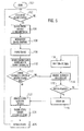
- a battery charge process is started at step 100. If an identification device 18 is detected in step 102, the charge station (Fig. 1) switches its LF transmitter on in step 104 to drive air coil 14. In step 106, a battery charge command is sent. In step 108, charge is enabled. In step 110, the charge station sends charge information to the charge controller within device 18. If the charge controller in step 112 determines that the charge information was supplied and received, a battery charge loop is entered at step 114. In step 114, the charge controller measures the battery voltage VBAT. As long as the battery voltage is below the rated maximum, as determined in step 116, the charge process is continued with waiting step 118. Otherwise, the charge loop is exited at step 120 with Charge disabled.
- step 112 determines that no charge information was received, or if step 120 returned with Charge disabled, step 122 continues with a several minutes waiting period for the charge station. Thereafter, step 124, the LF transmitter in the charge station is switched off. A "Disable Charge" command is then issued in step 126, and the loop returns to step 102.
Landscapes
- Engineering & Computer Science (AREA)
- Power Engineering (AREA)
- Computer Networks & Wireless Communication (AREA)
- Charge And Discharge Circuits For Batteries Or The Like (AREA)
- Lock And Its Accessories (AREA)
Applications Claiming Priority (2)
| Application Number | Priority Date | Filing Date | Title |
|---|---|---|---|
| DE20303301U | 2003-02-28 | ||
| DE20303301U DE20303301U1 (de) | 2003-02-28 | 2003-02-28 | Stromversorgung von elektronischen Systemen, die sowohl induktiv als auch aus einer wiederaufladbaren Batterie gespeist werden |
Publications (3)
| Publication Number | Publication Date |
|---|---|
| EP1452998A2 true EP1452998A2 (de) | 2004-09-01 |
| EP1452998A3 EP1452998A3 (de) | 2005-08-10 |
| EP1452998B1 EP1452998B1 (de) | 2007-12-19 |
Family
ID=27618958
Family Applications (1)
| Application Number | Title | Priority Date | Filing Date |
|---|---|---|---|
| EP20040100781 Expired - Lifetime EP1452998B1 (de) | 2003-02-28 | 2004-02-27 | Steuerschaltung zur Spannungsversorgung |
Country Status (4)
| Country | Link |
|---|---|
| US (1) | US7380150B2 (de) |
| EP (1) | EP1452998B1 (de) |
| JP (1) | JP2004266997A (de) |
| DE (2) | DE20303301U1 (de) |
Cited By (1)
| Publication number | Priority date | Publication date | Assignee | Title |
|---|---|---|---|---|
| US9660703B1 (en) | 2016-05-04 | 2017-05-23 | Dialog Semiconductor (Uk) Limited | Electronic circuit and system for wireless charging |
Families Citing this family (27)
| Publication number | Priority date | Publication date | Assignee | Title |
|---|---|---|---|---|
| US9130602B2 (en) * | 2006-01-18 | 2015-09-08 | Qualcomm Incorporated | Method and apparatus for delivering energy to an electrical or electronic device via a wireless link |
| US8447234B2 (en) | 2006-01-18 | 2013-05-21 | Qualcomm Incorporated | Method and system for powering an electronic device via a wireless link |
| DE112007001222B4 (de) * | 2006-05-26 | 2017-10-05 | Murata Manufacturing Co., Ltd. | Datenkoppler |
| US9652709B2 (en) | 2006-10-31 | 2017-05-16 | Fiber Mountain, Inc. | Communications between multiple radio frequency identification (RFID) connected tags and one or more devices, and related systems and methods |
| US9652708B2 (en) | 2006-10-31 | 2017-05-16 | Fiber Mountain, Inc. | Protocol for communications between a radio frequency identification (RFID) tag and a connected device, and related systems and methods |
| US9652707B2 (en) | 2006-10-31 | 2017-05-16 | Fiber Mountain, Inc. | Radio frequency identification (RFID) connected tag communications protocol and related systems and methods |
| US10032102B2 (en) * | 2006-10-31 | 2018-07-24 | Fiber Mountain, Inc. | Excess radio-frequency (RF) power storage in RF identification (RFID) tags, and related systems and methods |
| US9774086B2 (en) | 2007-03-02 | 2017-09-26 | Qualcomm Incorporated | Wireless power apparatus and methods |
| US9124120B2 (en) | 2007-06-11 | 2015-09-01 | Qualcomm Incorporated | Wireless power system and proximity effects |
| CN101842962B (zh) * | 2007-08-09 | 2014-10-08 | 高通股份有限公司 | 增加谐振器的q因数 |
| EP2188863A1 (de) | 2007-09-13 | 2010-05-26 | QUALCOMM Incorporated | Maximierung des pulverertrags aus drahtlosen leistungsmagnetresonatoren |
| EP2201641A1 (de) | 2007-09-17 | 2010-06-30 | Qualcomm Incorporated | Sender und empfänger für drahtlosen energietransfer |
| EP2208279A4 (de) * | 2007-10-11 | 2016-11-30 | Qualcomm Inc | Drahtloser stromtransfer unter verwendung von magnetomechanischen systemen |
| US8629576B2 (en) | 2008-03-28 | 2014-01-14 | Qualcomm Incorporated | Tuning and gain control in electro-magnetic power systems |
| DE102009021329B4 (de) * | 2009-05-14 | 2018-02-01 | Texas Instruments Deutschland Gmbh | Halbduplex-RFID-Transponder und Verfahren zum Betreiben eines Halbduplex-RFID-Transponders |
| DE102011100095B4 (de) * | 2011-04-29 | 2014-12-24 | Gottfried Wilhelm Leibniz Universität Hannover | Transpondereinheit |
| US9533230B2 (en) | 2011-05-16 | 2017-01-03 | Disney Enterprises, Inc. | Ghost expressions based on ghost data augmented by user-provided information |
| KR20140144174A (ko) * | 2012-01-05 | 2014-12-18 | 아닥 플라스틱스 인코포레이티드 | 차량 접근 시스템 |
| US20130249301A1 (en) * | 2012-03-21 | 2013-09-26 | Disney Enterprises, Inc., A Delaware Corporation | System And Method For Powering An RFID Module Using An Energy Harvesting Element |
| US9563832B2 (en) | 2012-10-08 | 2017-02-07 | Corning Incorporated | Excess radio-frequency (RF) power storage and power sharing RF identification (RFID) tags, and related connection systems and methods |
| US9069959B2 (en) * | 2012-12-21 | 2015-06-30 | Nxp B.V. | Cryptographic circuit protection from differential power analysis |
| US9601267B2 (en) | 2013-07-03 | 2017-03-21 | Qualcomm Incorporated | Wireless power transmitter with a plurality of magnetic oscillators |
| US9760747B2 (en) * | 2014-03-11 | 2017-09-12 | Canon Kabushiki Kaisha | Communication apparatus and method for controlling the same |
| JP6438245B2 (ja) * | 2014-09-05 | 2018-12-12 | キヤノン株式会社 | 通信装置およびその制御方法、プログラム |
| CN106541850B (zh) * | 2015-09-18 | 2020-05-22 | 比亚迪股份有限公司 | 用于电动车远程锁止的控制器、控制方法和控制系统 |
| EP3866292A1 (de) * | 2020-02-14 | 2021-08-18 | Soltec Innovations, S.L. | Sonnenfolgerleistungsverwaltung |
| DE102025125691A1 (de) | 2025-07-02 | 2026-04-02 | Mercedes-Benz Group AG | Verfahren zum Betreiben eines Schließsystems eines Kraftwagens sowie Schließsystem und Kommunikationseinheit |
Family Cites Families (10)
| Publication number | Priority date | Publication date | Assignee | Title |
|---|---|---|---|---|
| US4401894A (en) * | 1980-12-24 | 1983-08-30 | Professional Products, Inc. | Automatic uninterrupted D.C. power source switch |
| JPS58500820A (ja) * | 1981-05-27 | 1983-05-19 | マステク、コ−パレイシヤン | 集積回路作動方法および集積回路作動電力制御回路 |
| US4692604A (en) * | 1984-10-25 | 1987-09-08 | American Telephone And Telegraph Company, At&T Bell Laboratories | Flexible inductor |
| US5285779A (en) * | 1992-03-27 | 1994-02-15 | Hewlett-Packard Company | Method and apparatus for a cardiac defibrillator high voltage charging circuit |
| JPH0869513A (ja) | 1994-08-30 | 1996-03-12 | Mitsubishi Denki Semiconductor Software Kk | 非接触icカード |
| US6489883B1 (en) | 1997-04-30 | 2002-12-03 | Matsushita Electric Industrial Co., Ltd. | Non-contact data carrier system |
| US6188309B1 (en) * | 1998-01-07 | 2001-02-13 | At&T Corp | Method and apparatus for minimizing credit card fraud |
| US6275681B1 (en) * | 1998-04-16 | 2001-08-14 | Motorola, Inc. | Wireless electrostatic charging and communicating system |
| US7065658B1 (en) * | 2001-05-18 | 2006-06-20 | Palm, Incorporated | Method and apparatus for synchronizing and recharging a connector-less portable computer system |
| US20030019942A1 (en) * | 2001-07-24 | 2003-01-30 | Blossom George W. | System and method for electronically readable card having power source |
-
2003
- 2003-02-28 DE DE20303301U patent/DE20303301U1/de not_active Expired - Lifetime
-
2004
- 2004-02-25 US US10/787,611 patent/US7380150B2/en not_active Expired - Lifetime
- 2004-02-27 EP EP20040100781 patent/EP1452998B1/de not_active Expired - Lifetime
- 2004-02-27 DE DE200460010730 patent/DE602004010730T2/de not_active Expired - Lifetime
- 2004-02-27 JP JP2004053747A patent/JP2004266997A/ja active Pending
Cited By (1)
| Publication number | Priority date | Publication date | Assignee | Title |
|---|---|---|---|---|
| US9660703B1 (en) | 2016-05-04 | 2017-05-23 | Dialog Semiconductor (Uk) Limited | Electronic circuit and system for wireless charging |
Also Published As
| Publication number | Publication date |
|---|---|
| EP1452998A3 (de) | 2005-08-10 |
| DE602004010730D1 (de) | 2008-01-31 |
| DE20303301U1 (de) | 2003-07-17 |
| DE602004010730T2 (de) | 2008-12-24 |
| JP2004266997A (ja) | 2004-09-24 |
| US7380150B2 (en) | 2008-05-27 |
| EP1452998B1 (de) | 2007-12-19 |
| US20040189263A1 (en) | 2004-09-30 |
Similar Documents
| Publication | Publication Date | Title |
|---|---|---|
| US7380150B2 (en) | Method for selecting an inductive or battery power supply based on the voltage sensed therefrom for a transponder system | |
| US8774714B2 (en) | External power supply system for a lock comprising NFC-type contactless communication means | |
| US10036182B2 (en) | Electronic locking system | |
| US8222990B2 (en) | Hybrid access control system and method for controlling the same | |
| US20040080299A1 (en) | Energy source recharging device and method | |
| JP3564636B2 (ja) | トランスポンダ装置 | |
| CN100458841C (zh) | 一种支持无线充电的半有源射频识别标签 | |
| US6400255B1 (en) | Vehicle lock apparatus | |
| US20040227619A1 (en) | Electronic circuit for contactless tag, and contactless tag | |
| KR20100017735A (ko) | 축전지를 모니터링하기 위한 장치 | |
| TW201448320A (zh) | 電池裝置 | |
| US7692529B2 (en) | Passive entry and immobilizer at different frequencies using same antenna coil | |
| EP3889917B1 (de) | System und verfahren zur optimierten backup-funktionalität für elektronischen steuerschlüssel | |
| US20090127934A1 (en) | Emergency capacitor for a contactless device | |
| EP2700531B1 (de) | Ladesystem mit Diebstahlschutz | |
| CN110944884B (zh) | 移动标识发射器 | |
| CN102270314A (zh) | 非接触式控制方法及其装置 | |
| JP2002158041A (ja) | スライドドア内蔵用バッテリーに対する充電方法 | |
| US8471547B2 (en) | Circuit arrangement and method for inductive energy transfer | |
| JP2016197964A (ja) | 電子機器 | |
| CN108334920B (zh) | 一种用于车辆收费的复合智能卡及其供电管理方法 | |
| CN113965513B (zh) | 用于激活nfc设备的电路和方法 | |
| KR20050081503A (ko) | 절전형 알에프 아이디 태그 | |
| EP0778183A1 (de) | Vorrichtung zur Stromversorgung einer Fernbedienungseinheit | |
| US7317297B1 (en) | Battery temperature sensor pin used as communication channel |
Legal Events
| Date | Code | Title | Description |
|---|---|---|---|
| PUAI | Public reference made under article 153(3) epc to a published international application that has entered the european phase |
Free format text: ORIGINAL CODE: 0009012 |
|
| AK | Designated contracting states |
Kind code of ref document: A2 Designated state(s): AT BE BG CH CY CZ DE DK EE ES FI FR GB GR HU IE IT LI LU MC NL PT RO SE SI SK TR |
|
| AX | Request for extension of the european patent |
Extension state: AL LT LV MK |
|
| PUAL | Search report despatched |
Free format text: ORIGINAL CODE: 0009013 |
|
| AK | Designated contracting states |
Kind code of ref document: A3 Designated state(s): AT BE BG CH CY CZ DE DK EE ES FI FR GB GR HU IE IT LI LU MC NL PT RO SE SI SK TR |
|
| AX | Request for extension of the european patent |
Extension state: AL LT LV MK |
|
| RIC1 | Information provided on ipc code assigned before grant |
Ipc: 7G 06K 19/07 A Ipc: 7B 60R 25/04 B |
|
| 17P | Request for examination filed |
Effective date: 20060210 |
|
| AKX | Designation fees paid |
Designated state(s): DE FR GB |
|
| GRAP | Despatch of communication of intention to grant a patent |
Free format text: ORIGINAL CODE: EPIDOSNIGR1 |
|
| GRAS | Grant fee paid |
Free format text: ORIGINAL CODE: EPIDOSNIGR3 |
|
| GRAA | (expected) grant |
Free format text: ORIGINAL CODE: 0009210 |
|
| AK | Designated contracting states |
Kind code of ref document: B1 Designated state(s): DE FR GB |
|
| REG | Reference to a national code |
Ref country code: GB Ref legal event code: FG4D |
|
| REF | Corresponds to: |
Ref document number: 602004010730 Country of ref document: DE Date of ref document: 20080131 Kind code of ref document: P |
|
| ET | Fr: translation filed | ||
| PLBE | No opposition filed within time limit |
Free format text: ORIGINAL CODE: 0009261 |
|
| STAA | Information on the status of an ep patent application or granted ep patent |
Free format text: STATUS: NO OPPOSITION FILED WITHIN TIME LIMIT |
|
| 26N | No opposition filed |
Effective date: 20080922 |
|
| REG | Reference to a national code |
Ref country code: FR Ref legal event code: PLFP Year of fee payment: 13 |
|
| REG | Reference to a national code |
Ref country code: FR Ref legal event code: PLFP Year of fee payment: 14 |
|
| REG | Reference to a national code |
Ref country code: FR Ref legal event code: PLFP Year of fee payment: 15 |
|
| REG | Reference to a national code |
Ref country code: DE Ref legal event code: R082 Ref document number: 602004010730 Country of ref document: DE Representative=s name: ZELLER, ANDREAS, DE |
|
| PGFP | Annual fee paid to national office [announced via postgrant information from national office to epo] |
Ref country code: FR Payment date: 20230119 Year of fee payment: 20 |
|
| PGFP | Annual fee paid to national office [announced via postgrant information from national office to epo] |
Ref country code: GB Payment date: 20230121 Year of fee payment: 20 Ref country code: DE Payment date: 20230119 Year of fee payment: 20 |
|
| P01 | Opt-out of the competence of the unified patent court (upc) registered |
Effective date: 20230523 |
|
| REG | Reference to a national code |
Ref country code: DE Ref legal event code: R071 Ref document number: 602004010730 Country of ref document: DE |
|
| REG | Reference to a national code |
Ref country code: GB Ref legal event code: PE20 Expiry date: 20240226 |
|
| PG25 | Lapsed in a contracting state [announced via postgrant information from national office to epo] |
Ref country code: GB Free format text: LAPSE BECAUSE OF EXPIRATION OF PROTECTION Effective date: 20240226 |