EP1453227A2 - Dynamische Steuerung des Qualitätsverlustes von optischen Signalen in einem transparenten optischen Kommunikationsnetzwerk - Google Patents
Dynamische Steuerung des Qualitätsverlustes von optischen Signalen in einem transparenten optischen Kommunikationsnetzwerk Download PDFInfo
- Publication number
- EP1453227A2 EP1453227A2 EP03293295A EP03293295A EP1453227A2 EP 1453227 A2 EP1453227 A2 EP 1453227A2 EP 03293295 A EP03293295 A EP 03293295A EP 03293295 A EP03293295 A EP 03293295A EP 1453227 A2 EP1453227 A2 EP 1453227A2
- Authority
- EP
- European Patent Office
- Prior art keywords
- channels
- signals
- degradation
- line
- node
- Prior art date
- Legal status (The legal status is an assumption and is not a legal conclusion. Google has not performed a legal analysis and makes no representation as to the accuracy of the status listed.)
- Granted
Links
Images


Classifications
-
- H—ELECTRICITY
- H04—ELECTRIC COMMUNICATION TECHNIQUE
- H04B—TRANSMISSION
- H04B10/00—Transmission systems employing electromagnetic waves other than radio-waves, e.g. infrared, visible or ultraviolet light, or employing corpuscular radiation, e.g. quantum communication
- H04B10/07—Arrangements for monitoring or testing transmission systems; Arrangements for fault measurement of transmission systems
- H04B10/075—Arrangements for monitoring or testing transmission systems; Arrangements for fault measurement of transmission systems using an in-service signal
- H04B10/079—Arrangements for monitoring or testing transmission systems; Arrangements for fault measurement of transmission systems using an in-service signal using measurements of the data signal
- H04B10/0795—Performance monitoring; Measurement of transmission parameters
- H04B10/07953—Monitoring or measuring OSNR, BER or Q
-
- H—ELECTRICITY
- H04—ELECTRIC COMMUNICATION TECHNIQUE
- H04B—TRANSMISSION
- H04B10/00—Transmission systems employing electromagnetic waves other than radio-waves, e.g. infrared, visible or ultraviolet light, or employing corpuscular radiation, e.g. quantum communication
- H04B10/07—Arrangements for monitoring or testing transmission systems; Arrangements for fault measurement of transmission systems
- H04B10/075—Arrangements for monitoring or testing transmission systems; Arrangements for fault measurement of transmission systems using an in-service signal
- H04B10/079—Arrangements for monitoring or testing transmission systems; Arrangements for fault measurement of transmission systems using an in-service signal using measurements of the data signal
- H04B10/0793—Network aspects, e.g. central monitoring of transmission parameters
-
- H—ELECTRICITY
- H04—ELECTRIC COMMUNICATION TECHNIQUE
- H04J—MULTIPLEX COMMUNICATION
- H04J14/00—Optical multiplex systems
- H04J14/02—Wavelength-division multiplex systems
- H04J14/0221—Power control, e.g. to keep the total optical power constant
- H04J14/02216—Power control, e.g. to keep the total optical power constant by gain equalization
-
- H—ELECTRICITY
- H04—ELECTRIC COMMUNICATION TECHNIQUE
- H04B—TRANSMISSION
- H04B2210/00—Indexing scheme relating to optical transmission systems
- H04B2210/25—Distortion or dispersion compensation
- H04B2210/254—Distortion or dispersion compensation before the transmission line, i.e. pre-compensation
Definitions
- the invention relates to the field of optical transmission of signals within so-called length-switching optical networks "or" wavelength band switching ", also called transparent networks.
- Optimizing channel performance balancing is nevertheless possible, in theory, in this type of transparent network when there are certain parameters associated with the signals of each channel and related to their quality, such as the error rate or the signal ratio optical noise (or OSNR for “Optical Signal to Noise Ratio”) and the power level (or optical power). But this is rarely the case.
- the performance of the channels is optimized on the longest path in the network, when it was designed.
- we determines at the end of the longest path the values of the OSNRs associated with certain selected channels for example using analyzers optical spectrum (or OSAs for “Optical Spectrum Analyzers”) or dedicated equipment, such as optical performance controllers (or OPM for “Optical Performance Monitor”), while maintaining the others channels at predefined power levels taking into account network characteristics.
- the invention therefore aims to improve the situation.
- node means communications equipment responsible for switching and / or routing wavelengths or wavelength bands within a transparent network. He can therefore be a brewer (or “cross-connect”).
- the profile of power in a network node which is placed at an upstream end of the transmission line is preferentially applied not on the received signals which have been the subject determining the value of the degradation parameter, but on the next signals which must circulate in the transmission line.
- the parameter values of degradation in step b) are included in an interval of width (or amplitude tolerance) chosen (possibly zero).
- the network is wavelength band switching, equalizing in each line of transmission the gains of the channels of the different bands as a function of their respective wavelengths, before receiving the signals at the level of the node considered.
- the invention also relates to a device for controlling degradation parameters, such as ⁇ OSNR, associated with channel signals of distinct wavelengths, possibly arranged in channel strips, and transmitted by transmission lines connecting between them the nodes of an optical communications network of the type Trnsprncy
- This device is characterized by the fact that it includes means for loaded processing, if at least two signals are transmitted channels or channel strips by one or more transmission lines, from measure for each of these channels, or each of these channel strips, on the one hand, the value of a parameter (for example ⁇ OSNR) representative of the degradation of the signals in the line, and on the other hand, taking into account the measured values, a power profile to be imposed on the signals so that they have predetermined degradation parameter values.
- a parameter for example ⁇ OSNR
- the processing means are arranged to so as to choose the degradation parameter values so that they are included in a width interval (or amplitude tolerance) chosen (possibly null).
- the means of processing are arranged so as to repeat the determination of values degradation parameter, for example by varying a step of processing, until the degradation parameter values are included in the chosen interval.
- the means of processing include a power control module arranged to so as to impose the determined power profiles on the signals, correspondents, before they are entered into a line of outgoing transmission.
- this control module of power is designed to impose determined power profiles in a network node which is placed at an upstream end of the line transmission considered.
- Such a control device can for example be integrated into a communications equipment of a transparent network, of node type or management server. It can thus act either on a node, locally, or on a multiplicity of nodes, centrally.
- the invention relates to optical communications networks.
- transparent be they of the so-called “wavelength switching type” or “wavelength band switching", for example “wavelength division multiplexing” (or WDM) networks for “Wavelength Division Multiplexing”) and “multiplexing by dense distribution of wavelengths "(or DWDM for" Dense Wavelength Division Multiplexing ”).
- WDM wavelength division multiplexing
- DWDM Dense Wavelength Division Multiplexing
- E servers or brewers or “cross-connects”
- An optical transmission line Lj is generally formed one or more portions of lines, also called “spans", comprising one or more optical fibers coupled to an amplifier optical. Each optical fiber is capable of transmitting signals from C channels to which particular wavelengths are assigned.
- C channels are grouped into bands of substantially constant width, in which they are substantially equidistant from each other.
- the brewers constitute optical nodes Ni responsible for ensuring switching and / or routing of wavelengths or bands wavelengths within the transparent network.
- a brewer can be by example of the so-called "insertion and / or extraction” (or "Add / Drop") type of resources, especially optical.
- a resource can be either a data packet or a wavelength, again a band of wavelengths.
- a transmission line Lj connecting two neighboring nodes Ni can therefore be seen as a cascade of spans that introduces degradation signals between these two nodes and, therefore, inhomogeneities performance between channels when they have passed through different transmission lines.
- the invention aims to allow the optimization of the balancing of performance between channels.
- each node Ni of the transparent network is equipped with a device Di according to the invention, charged to optimize the performance of the channels which reach it from one or several so-called “incoming” lines and which it must retransmit on one or several so-called “outgoing” lines.
- a device D installed, for example, in a server of network management, and responsible for acting on all the nodes of the network so centralized.
- the transparent network is wavelength switching.
- the control device Di includes a PMi processing module loaded, when transmitting signals from at least two channels or bands by a transmission line Lj, at the ends of which are placed an upstream node Ni, in which it is implanted, and a downstream node Ni ', of determine for each of these channels, on the one hand, the value of a parameter representative of the degradation of the signals in the corresponding line, and on the other hand, taking into account the determined values, a power profile to impose on the signals so that they have a value of degradation parameter chosen.
- control device D2 which is installed in the node N2.
- the node N2 is connected, of a first part, at node N1 by the transmission line L1, of a second share, to the server E by the transmission line L2, thirdly, to the node N3 via the transmission line L3, and on the other hand, to the node N4 via the L4 transmission line.
- the node N1 has received on one of its insertion ports three channels C1 of different wavelengths carrying signals which it must transmit to the node N4, via the node N2.
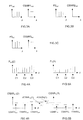
- the signals of these three channels C1 are introduced into line L1, along arrow F1, with powers (P1 out ) and an optical signal to noise ratio or OSNR for "Optical Signal to Noise Ratio" (OSNR1 out ), represented on FIG. 3A as a function of the wavelength ⁇ .
- the signal strengths of the three channels C1 are different, but it could be otherwise.
- the OSNR is the same here for the signals of the three C1 channels, but it could be otherwise.
- the server E wants to transmit to the node N4, via the node N2, signals from three channels C2 of distinct wavelengths.
- the signals of these three channels C2 are introduced into line L2, along arrow F2, with powers (P2 out ) and an OSNR (OSNR2 out ), represented in FIG. 3B as a function of the wavelength ⁇ .
- P2 out powers
- OSNR2 out OSNR
- FIG. 3B the signal strengths of the three C2 channels are different, but it could be otherwise.
- the OSNR is the same here for the signals of the three C2 channels, but it could be otherwise.
- the node N3 has received on one of its insertion ports three channels C3 of distinct wavelengths carrying signals which it must transmit to the node N4, via the node N2.
- the signals of these three channels C3 are introduced into line L3, along arrow F3, with powers (P3 out ) and an OSNR (OSNR3 out ), represented in FIG. 3C as a function of the wavelength ⁇ .
- the signal strengths of the three C3 channels are different, but it could be otherwise.
- the OSNR is here the same for the signals of the three C3 channels, but it could be otherwise.
- the different signals of channels C1, C2 and C3 therefore flow in lines L1, L2 and L3, and reach the input ports of node N2 according to arrows F'1, F'2 and F'3, respectively.
- the channels exhibit inhomogeneous performance because they have taken on different lines.
- the degradation parameter used by the PM2 processing module of the D2 device to optimize the channel performance C is the variation of OSNR ( ⁇ OSNR).
- ⁇ OSNR OSNR
- House could use another parameter, such as the rate variation errors or quality factor (Q) or deformation of the "eye” (superposition of all the frames of 0 and 1 which circulate on a line).
- the powers (P out (2)) and the OSNRs (OSNR out (2)) of the signals of the channels C1, C2 and C3 at the output of the node N2 are respectively grouped in FIGS. 4A and 4B.
- the powers (P in (4)) and OSNRs (OSNR in (4)) of the signals contained in the channels C1, C2 and C3 at the input of the node N4 are respectively grouped in FIGS. 5A and 5B.
- Figures 4A and 5A thus materialize the power variations channels C1, C2 and C3 between the input (fig. 4A) and the output (fig. 5A) of the line L4, before treatment with the device according to the invention.
- the figures 4B and 5B materialize the variations ( ⁇ OSNR (1)) of the OSNRs of the different channels (C1, C2 and C3) induced by the cascade of spans in line L4, before treatment with the device according to the invention.
- the measurement of the degradations introduced by the line considered that is to say, here, the determination of the variations of OSNR ( ⁇ OSNR (1)), also called degradation parameter values, is performed by a first calculation module CM1 which preferably forms part of the processing module PM2 (although this is not compulsory).
- CM1 which preferably forms part of the processing module PM2 (although this is not compulsory).
- Many techniques well known to those skilled in the art, make it possible to determine at the level of a node Ni the OSNRs and the powers associated with the signals (Si out ) contained in the different channels received and transmitted, and deduce the variations of OSNR ( ⁇ OSNR) induced by the transmission lines Lj to which this node Ni is connected. Since these techniques are not the subject of the invention, they are therefore not described here. For example, one can use the technique called optical power control (or OPM for "Optical Performance Monitoring").
- the first calculation module CM1 of node N2 is in possession of the OSNRs of channels C1, C2 and C3 at the output of node N2 (OSNR1 out (2), OSNR2 out (2) and OSNR3 out (2)) and at the input of node N4 (OSNR1 in (4), OSNR2 in (4) and OSNR3 in (4)), it communicates them to a comparison module CM2 of the processing module PM2 of node N2, responsible for comparing them with each other .
- the CM2 comparison module is responsible for compare the values of the input and output OSNRs of each channel, received from the first CM1 calculation module, to determine their deviations ( ⁇ OSNR) and compare these deviations to a chosen width interval (or selected amplitude tolerance). This width (or amplitude) can be chosen as small as desired. It can even be zero.
- the module CM2 comparator communicates them to a second CM3 calculation module, responsible for determining for each channel, taking into account the associated OSNRs, a power profile to be imposed on the signals so that they have an ⁇ OSNR (2) of a chosen value at the exit of line L4.
- the second module of calculation decides not to modify the signal strengths of the C1 channels and C2, but to reduce the signal strength of the channels by a value ⁇ P3 C3.
- this variation ⁇ P3 reinforces the relative value of the signals of channels C1 and C3, which results in a slight increase in noise added to C3 channels and a significant reduction of noise added to channels C1 and C2. This translates directly by a variation in degradation of OSNR on line L4.
- the output OSNRs OSNR1 out (2), OSNR2 out (2) and OSNR3 out (2) of channels C1, C2 and C3 are not equal (which is usually the case). However, this does not prevent equalizing the degradation of the OSNR on the L4 line.
- each power profile is preferably applied not to the signals received by the node N4, but on the next signals which must circulate in the line of transmission L4 and which will be received by node N4 later. In in other words, we perform the detection on signals and apply the profile determined at the following signals.
- each CM4 power control module includes an attenuation module, responsible for applying a spectrum to the signals attenuation adapted to the determined power profile, which may have a variable form, any.
- the profiles have been applied to the following signals, in the node N2, they are communicated to the first calculation module CM1 which determines their respective OSNRs, then communicates them to the CM2 comparison, so that it checks that said corresponding ⁇ OSNRs are included in the width range (or amplitude tolerance) chosen.
- the PM2 processing module can be arranged to operate in iterative mode. More precisely, as long as convergence is not obtained, that is, as long as the measured ⁇ OSNRs are not all included in the width interval (or amplitude tolerance) chosen, the PM2 processing performs processing loops (CM2 ⁇ CM3 ⁇ CM4 ⁇ CM1 ⁇ CM2).
- processing loops can adapt the calculation methods of the second CM3 calculation module to the state of system, possibly taking into account its past, using algorithms can be very complex. For example, we can vary each completes the step of the calculation algorithm implemented by the second module of CM3 calculation.
- Each loop is performed on different signals which have the profiles determined on the previous loop have been applied.
- FIGS. 6A and 7A have been placed on the same level in order to facilitate the observation of the variations in the power levels of the different channels (C1, C2 and C3) induced by the cascade of spans of the line L4, after treatment by the device. according to the invention.
- FIGS. 6B and 7B have been placed on the same level in order to facilitate the observation of the variations ( ⁇ OSNR (2)) of the OSNRs of the different channels (C1, C2 and C3) induced by the cascade of spans of the line. L4, after treatment with the device according to the invention.
- P in (4), OSNR in (4) and ⁇ OSNR (2) respectively designate the signal power on the input ports of node N4, the OSNR signals on the input ports of node N4 and the variation in OSNR (or degradation) introduced by line L4, after treatment by the device according to the invention.
- the variation of OSNR ( ⁇ OSNR 1 (2)) undergone by the channels C1 is substantially identical to the variation of OSNR ( ⁇ OSNR 2 (2)) undergone by the channels C2, which is substantially identical to the variation in OSNR ( ⁇ OSNR 3 (2)) undergone by the channels C3.
- the gap which existed at the output of node N2 between the OSNR3 out (2), on the one hand, and the OSNR1 out (2) and OSNR2 out (2) has been substantially maintained (or preserved ) until the entrance to node N4.
- the Di control device implanted in a Ni node it may be advantageous to equalize the gains of channels upstream of said Ni node, according to their wavelengths respectively. This is particularly useful when the network is wavelength band switching.
- This gain equalization is a technique well known to man. art. Therefore it will not be described here. It is preferentially carried out by filters coupled to the relay amplifiers installed on the transmission lines.
- control device D has to process multiplexes comprising several wavelength bands each comprising several equidistant channels, for example 5, the processing is substantially identical. It suffices to consider each band as a channel, and therefore determine the OSNR associated with each band and then the profile of power to be imposed on each band taking into account the associated OSNRs to the different bands received.
- the control device D and more precisely its first CM1 and second CM3 calculation modules, its CM2 comparison module and its CM4 power control module, can be realized in the form of electronic circuits (or “hardware”), software modules or computer (or “software”), or a combination of circuits and software.
- the invention also provides a method for controlling the parameters of degradation, such as ⁇ OSNRs, associated with Si signals circulating in Ck channels of distinct wavelengths, possibly arranged in channel strips, and defined in Lj transmission lines connecting together the nodes Ni of an optical communications network of transparent type.
- ⁇ OSNRs parameters of degradation
- the main and optional functions and sub-functions provided by the steps of this process being substantially identical to those provided by the different means constituting the control device D and / or the network transparent, only the steps implementing the main functions of the method according to the invention.
- step b) the values of degradation parameter so that they are included in an interval width (or amplitude tolerance) chosen (possibly zero).
- an iterative mechanism consisting of repeat steps a) and b), for example by varying a step each time processing, until the degradation parameter values are all included in the interval (or tolerance) chosen.
- the complex problem of optimizing channel performance of a transparent network is segmented and by therefore easier to perform. This segmentation also facilitates optimization of network design, transmission line after line of transmission.
- optimization is now compatible, on the one hand, with the adjustments of the transmission imposed by their aging, and on the other hand, with routing reconfiguration.
- the invention allows the global and simultaneous optimization of all channels.
- control device of the invention in which the n channels using the same transmission line had different powers but the same OSNR.
- control device of the invention is also suitable for the case where the n channels using the same transmission line have different powers and different OSNRs.
- an application of the device according to the invention for power control is not not limited to this parameter. It also concerns other parameters, such as chromatic dispersion, polarization state, wavelength fluctuation (or "chirping"), or phase state.
Landscapes
- Engineering & Computer Science (AREA)
- Computer Networks & Wireless Communication (AREA)
- Signal Processing (AREA)
- Physics & Mathematics (AREA)
- Electromagnetism (AREA)
- Optical Communication System (AREA)
- Glass Compositions (AREA)
Applications Claiming Priority (2)
| Application Number | Priority Date | Filing Date | Title |
|---|---|---|---|
| FR0300214A FR2849971A1 (fr) | 2003-01-10 | 2003-01-10 | Controle dynamique du niveau de degradation de signaux optiques dans un reseau de communication optique de type transparent |
| FR0300214 | 2003-01-10 |
Publications (3)
| Publication Number | Publication Date |
|---|---|
| EP1453227A2 true EP1453227A2 (de) | 2004-09-01 |
| EP1453227A3 EP1453227A3 (de) | 2005-08-31 |
| EP1453227B1 EP1453227B1 (de) | 2010-09-01 |
Family
ID=32524799
Family Applications (1)
| Application Number | Title | Priority Date | Filing Date |
|---|---|---|---|
| EP03293295A Expired - Lifetime EP1453227B1 (de) | 2003-01-10 | 2003-12-23 | Dynamische Steuerung des Qualitätsverlustes von optischen Signalen in einem transparenten optischen Kommunikationsnetzwerk |
Country Status (5)
| Country | Link |
|---|---|
| US (1) | US7574138B2 (de) |
| EP (1) | EP1453227B1 (de) |
| AT (1) | ATE480057T1 (de) |
| DE (1) | DE60333982D1 (de) |
| FR (1) | FR2849971A1 (de) |
Family Cites Families (7)
| Publication number | Priority date | Publication date | Assignee | Title |
|---|---|---|---|---|
| US6317231B1 (en) * | 1998-09-04 | 2001-11-13 | Lucent Technologies Inc. | Optical monitoring apparatus and method for network provisioning and maintenance |
| US20030063343A1 (en) * | 1999-09-03 | 2003-04-03 | Oni Systems Corp. | Optical power management in an optical network |
| US6400479B1 (en) * | 1999-12-20 | 2002-06-04 | Sycamore Networks, Inc. | Optical power balancer for optical amplified WDM networks |
| JP2001203414A (ja) * | 2000-01-18 | 2001-07-27 | Fujitsu Ltd | 光信号対雑音比測定方法、並びに、該測定方法を利用した光信号対雑音比測定装置、プリエンファシス方法、光通信システム、測定回路、および、制御装置 |
| IL141740A (en) * | 2001-03-01 | 2005-12-18 | Eci Telecom Ltd | Method and system for handling optical signals |
| US7081987B2 (en) * | 2002-05-29 | 2006-07-25 | Pts Corporation | Coordinated control of dynamic gain equalization in a wavelength division multiplexed optical system |
| US6668137B1 (en) * | 2002-06-26 | 2003-12-23 | Nortel Networks Limited | Feed forward optical power control |
-
2003
- 2003-01-10 FR FR0300214A patent/FR2849971A1/fr active Pending
- 2003-12-23 EP EP03293295A patent/EP1453227B1/de not_active Expired - Lifetime
- 2003-12-23 DE DE60333982T patent/DE60333982D1/de not_active Expired - Lifetime
- 2003-12-23 AT AT03293295T patent/ATE480057T1/de not_active IP Right Cessation
-
2004
- 2004-01-09 US US10/753,328 patent/US7574138B2/en active Active
Also Published As
| Publication number | Publication date |
|---|---|
| FR2849971A1 (fr) | 2004-07-16 |
| EP1453227A3 (de) | 2005-08-31 |
| US7574138B2 (en) | 2009-08-11 |
| EP1453227B1 (de) | 2010-09-01 |
| US20040179838A1 (en) | 2004-09-16 |
| ATE480057T1 (de) | 2010-09-15 |
| DE60333982D1 (de) | 2010-10-14 |
Similar Documents
| Publication | Publication Date | Title |
|---|---|---|
| FR2957735A1 (fr) | Procede d'optimisation de la capacite des reseaux optiques de communication | |
| CA2276905A1 (fr) | Amplification quasi-distribuee dans un systeme de transmission a fibre optique a signaux solitons | |
| EP3614580A1 (de) | Schaltkreis zum verbinden eines lokalen netzwerks mit einer optischen faser, auf der lichtsignale geleitet werden können, die unterschiedlichen optischen kommunikationsstandards entsprechen | |
| EP1434376B1 (de) | Verfahren und Vorrichtung zur Regelung der Ausgangsleistung eines Knotens in einem optischen Wellenlängenkopplungsneztwerk | |
| EP2070382A1 (de) | Verfahren zur verwaltung von verbindungen in einem optischen zugangsnetzwerk sowie plattform, ersatzteile, netzwerk und computersoftwareprodukt dafür | |
| FR2812988A1 (fr) | Commutateur de signaux optiques | |
| EP0802640B1 (de) | Verfahren und Vorrichtung zur Verstärkung von aus Wellenlängenmultiplex aufbereiteten Kanälen | |
| EP1453227B1 (de) | Dynamische Steuerung des Qualitätsverlustes von optischen Signalen in einem transparenten optischen Kommunikationsnetzwerk | |
| FR2832274A1 (fr) | Procede de controle dynamique d'un module optique | |
| EP1428333B1 (de) | Optisches ringnetzwerk mit doppeltem optischem bus | |
| EP3753259B1 (de) | Steuerungsebene für ein optisches netzwerk zur übertragung von mehrträgerdatenbursts mit dynamischer anpassung der lernsequenz | |
| EP1497939A1 (de) | Optische vorrichtung und verfahren zur umwandlung eines wdm-signals in ein otdm-signal und umgekehrt | |
| EP4233209A1 (de) | Entzerrungsverfahren in einem zugangsnetzwerk vom passiven optischen netzwerktyp, computerprogrammprodukt, optischer leitungsabschluss und entsprechende optische netzwerkeinheit | |
| FR2829629A1 (fr) | Amplificateur optique a faible bruit et systeme de communication optique l'utilisant | |
| Otero-Casado et al. | Impact of Subcarrier-Routing Devices on the Performance of DSCM Coherent Systems Evaluated with Analytical Models | |
| EP3545631B1 (de) | Bestimmung von regenerativen relaisknoten in einer übertragungsleitung eines optischen netzwerks | |
| EP2239874B1 (de) | Vorrichtung zum Empfang von Kämmen mit Zwischenkanalfrequenzabstand | |
| EP1592159A2 (de) | Optisches Übertragungsnetz mit Baumstruktur | |
| WO2009112767A1 (fr) | Dispositif et procédé de gestion de la puissance d'émission d'une source optique en fonction du niveau de pertes optiques d'une liaison optique | |
| FR2782588A1 (fr) | Dispositif d'insertion/extraction de signaux optiques multiplexes en longueur d'onde | |
| FR2935210A1 (fr) | Noeud de commutation de paquets optiques. | |
| EP0994594A1 (de) | Verfahren und Vorrichtung zum herausziehen und einsetzen von einem Kanal für optische WDM Übertragung | |
| EP1455551A2 (de) | Selektionsmodul für optische Schalter und optischer Schalter | |
| Al Zahr | Planification de réseaux WDM translucides avec qualité de transmission garantie | |
| EP0994585A1 (de) | Leistungsausgleich in einem wellenlängenmultiplexierten optischen Übertragungssystem mit mehreren Verstärkern |
Legal Events
| Date | Code | Title | Description |
|---|---|---|---|
| PUAI | Public reference made under article 153(3) epc to a published international application that has entered the european phase |
Free format text: ORIGINAL CODE: 0009012 |
|
| AK | Designated contracting states |
Kind code of ref document: A2 Designated state(s): AT BE BG CH CY CZ DE DK EE ES FI FR GB GR HU IE IT LI LU MC NL PT RO SE SI SK TR |
|
| AX | Request for extension of the european patent |
Extension state: AL LT LV MK |
|
| RTI1 | Title (correction) |
Free format text: DYNAMIC CONTROL OF DEGRADATION LEVEL OF OPTICAL SIGNALS IN A TRANSPARENT OPTICAL COMMUNICATIONS NETWORK |
|
| PUAL | Search report despatched |
Free format text: ORIGINAL CODE: 0009013 |
|
| AK | Designated contracting states |
Kind code of ref document: A3 Designated state(s): AT BE BG CH CY CZ DE DK EE ES FI FR GB GR HU IE IT LI LU MC NL PT RO SE SI SK TR |
|
| AX | Request for extension of the european patent |
Extension state: AL LT LV MK |
|
| RIC1 | Information provided on ipc code assigned before grant |
Ipc: 7H 04B 10/08 A Ipc: 7H 04B 10/17 B |
|
| 17P | Request for examination filed |
Effective date: 20060228 |
|
| AKX | Designation fees paid |
Designated state(s): AT BE BG CH CY CZ DE DK EE ES FI FR GB GR HU IE IT LI LU MC NL PT RO SE SI SK TR |
|
| 17Q | First examination report despatched |
Effective date: 20070213 |
|
| RAP1 | Party data changed (applicant data changed or rights of an application transferred) |
Owner name: ALCATEL LUCENT |
|
| GRAP | Despatch of communication of intention to grant a patent |
Free format text: ORIGINAL CODE: EPIDOSNIGR1 |
|
| GRAS | Grant fee paid |
Free format text: ORIGINAL CODE: EPIDOSNIGR3 |
|
| GRAA | (expected) grant |
Free format text: ORIGINAL CODE: 0009210 |
|
| AK | Designated contracting states |
Kind code of ref document: B1 Designated state(s): AT BE BG CH CY CZ DE DK EE ES FI FR GB GR HU IE IT LI LU MC NL PT RO SE SI SK TR |
|
| REG | Reference to a national code |
Ref country code: GB Ref legal event code: FG4D Free format text: NOT ENGLISH |
|
| REG | Reference to a national code |
Ref country code: CH Ref legal event code: EP |
|
| REG | Reference to a national code |
Ref country code: IE Ref legal event code: FG4D Free format text: LANGUAGE OF EP DOCUMENT: FRENCH |
|
| REF | Corresponds to: |
Ref document number: 60333982 Country of ref document: DE Date of ref document: 20101014 Kind code of ref document: P |
|
| REG | Reference to a national code |
Ref country code: NL Ref legal event code: VDEP Effective date: 20100901 |
|
| PG25 | Lapsed in a contracting state [announced via postgrant information from national office to epo] |
Ref country code: FI Free format text: LAPSE BECAUSE OF FAILURE TO SUBMIT A TRANSLATION OF THE DESCRIPTION OR TO PAY THE FEE WITHIN THE PRESCRIBED TIME-LIMIT Effective date: 20100901 Ref country code: AT Free format text: LAPSE BECAUSE OF FAILURE TO SUBMIT A TRANSLATION OF THE DESCRIPTION OR TO PAY THE FEE WITHIN THE PRESCRIBED TIME-LIMIT Effective date: 20100901 |
|
| PG25 | Lapsed in a contracting state [announced via postgrant information from national office to epo] |
Ref country code: CY Free format text: LAPSE BECAUSE OF FAILURE TO SUBMIT A TRANSLATION OF THE DESCRIPTION OR TO PAY THE FEE WITHIN THE PRESCRIBED TIME-LIMIT Effective date: 20100901 Ref country code: SI Free format text: LAPSE BECAUSE OF FAILURE TO SUBMIT A TRANSLATION OF THE DESCRIPTION OR TO PAY THE FEE WITHIN THE PRESCRIBED TIME-LIMIT Effective date: 20100901 |
|
| REG | Reference to a national code |
Ref country code: IE Ref legal event code: FD4D |
|
| PG25 | Lapsed in a contracting state [announced via postgrant information from national office to epo] |
Ref country code: NL Free format text: LAPSE BECAUSE OF FAILURE TO SUBMIT A TRANSLATION OF THE DESCRIPTION OR TO PAY THE FEE WITHIN THE PRESCRIBED TIME-LIMIT Effective date: 20100901 Ref country code: SE Free format text: LAPSE BECAUSE OF FAILURE TO SUBMIT A TRANSLATION OF THE DESCRIPTION OR TO PAY THE FEE WITHIN THE PRESCRIBED TIME-LIMIT Effective date: 20100901 Ref country code: GR Free format text: LAPSE BECAUSE OF FAILURE TO SUBMIT A TRANSLATION OF THE DESCRIPTION OR TO PAY THE FEE WITHIN THE PRESCRIBED TIME-LIMIT Effective date: 20101202 |
|
| PG25 | Lapsed in a contracting state [announced via postgrant information from national office to epo] |
Ref country code: IE Free format text: LAPSE BECAUSE OF FAILURE TO SUBMIT A TRANSLATION OF THE DESCRIPTION OR TO PAY THE FEE WITHIN THE PRESCRIBED TIME-LIMIT Effective date: 20100901 |
|
| PG25 | Lapsed in a contracting state [announced via postgrant information from national office to epo] |
Ref country code: PT Free format text: LAPSE BECAUSE OF FAILURE TO SUBMIT A TRANSLATION OF THE DESCRIPTION OR TO PAY THE FEE WITHIN THE PRESCRIBED TIME-LIMIT Effective date: 20110103 Ref country code: EE Free format text: LAPSE BECAUSE OF FAILURE TO SUBMIT A TRANSLATION OF THE DESCRIPTION OR TO PAY THE FEE WITHIN THE PRESCRIBED TIME-LIMIT Effective date: 20100901 Ref country code: IT Free format text: LAPSE BECAUSE OF FAILURE TO SUBMIT A TRANSLATION OF THE DESCRIPTION OR TO PAY THE FEE WITHIN THE PRESCRIBED TIME-LIMIT Effective date: 20100901 Ref country code: CZ Free format text: LAPSE BECAUSE OF FAILURE TO SUBMIT A TRANSLATION OF THE DESCRIPTION OR TO PAY THE FEE WITHIN THE PRESCRIBED TIME-LIMIT Effective date: 20100901 Ref country code: RO Free format text: LAPSE BECAUSE OF FAILURE TO SUBMIT A TRANSLATION OF THE DESCRIPTION OR TO PAY THE FEE WITHIN THE PRESCRIBED TIME-LIMIT Effective date: 20100901 Ref country code: SK Free format text: LAPSE BECAUSE OF FAILURE TO SUBMIT A TRANSLATION OF THE DESCRIPTION OR TO PAY THE FEE WITHIN THE PRESCRIBED TIME-LIMIT Effective date: 20100901 |
|
| BERE | Be: lapsed |
Owner name: ALCATEL LUCENT Effective date: 20101231 |
|
| PG25 | Lapsed in a contracting state [announced via postgrant information from national office to epo] |
Ref country code: ES Free format text: LAPSE BECAUSE OF FAILURE TO SUBMIT A TRANSLATION OF THE DESCRIPTION OR TO PAY THE FEE WITHIN THE PRESCRIBED TIME-LIMIT Effective date: 20101212 |
|
| PLBE | No opposition filed within time limit |
Free format text: ORIGINAL CODE: 0009261 |
|
| STAA | Information on the status of an ep patent application or granted ep patent |
Free format text: STATUS: NO OPPOSITION FILED WITHIN TIME LIMIT |
|
| PG25 | Lapsed in a contracting state [announced via postgrant information from national office to epo] |
Ref country code: MC Free format text: LAPSE BECAUSE OF NON-PAYMENT OF DUE FEES Effective date: 20101231 |
|
| REG | Reference to a national code |
Ref country code: CH Ref legal event code: PL |
|
| 26N | No opposition filed |
Effective date: 20110606 |
|
| PG25 | Lapsed in a contracting state [announced via postgrant information from national office to epo] |
Ref country code: DK Free format text: LAPSE BECAUSE OF FAILURE TO SUBMIT A TRANSLATION OF THE DESCRIPTION OR TO PAY THE FEE WITHIN THE PRESCRIBED TIME-LIMIT Effective date: 20100901 |
|
| PG25 | Lapsed in a contracting state [announced via postgrant information from national office to epo] |
Ref country code: BE Free format text: LAPSE BECAUSE OF NON-PAYMENT OF DUE FEES Effective date: 20101231 |
|
| REG | Reference to a national code |
Ref country code: DE Ref legal event code: R097 Ref document number: 60333982 Country of ref document: DE Effective date: 20110606 |
|
| PG25 | Lapsed in a contracting state [announced via postgrant information from national office to epo] |
Ref country code: LI Free format text: LAPSE BECAUSE OF NON-PAYMENT OF DUE FEES Effective date: 20101231 Ref country code: CH Free format text: LAPSE BECAUSE OF NON-PAYMENT OF DUE FEES Effective date: 20101231 |
|
| PG25 | Lapsed in a contracting state [announced via postgrant information from national office to epo] |
Ref country code: LU Free format text: LAPSE BECAUSE OF NON-PAYMENT OF DUE FEES Effective date: 20101223 Ref country code: BG Free format text: LAPSE BECAUSE OF FAILURE TO SUBMIT A TRANSLATION OF THE DESCRIPTION OR TO PAY THE FEE WITHIN THE PRESCRIBED TIME-LIMIT Effective date: 20100901 Ref country code: HU Free format text: LAPSE BECAUSE OF FAILURE TO SUBMIT A TRANSLATION OF THE DESCRIPTION OR TO PAY THE FEE WITHIN THE PRESCRIBED TIME-LIMIT Effective date: 20110302 |
|
| PG25 | Lapsed in a contracting state [announced via postgrant information from national office to epo] |
Ref country code: TR Free format text: LAPSE BECAUSE OF FAILURE TO SUBMIT A TRANSLATION OF THE DESCRIPTION OR TO PAY THE FEE WITHIN THE PRESCRIBED TIME-LIMIT Effective date: 20100901 |
|
| PG25 | Lapsed in a contracting state [announced via postgrant information from national office to epo] |
Ref country code: BG Free format text: LAPSE BECAUSE OF FAILURE TO SUBMIT A TRANSLATION OF THE DESCRIPTION OR TO PAY THE FEE WITHIN THE PRESCRIBED TIME-LIMIT Effective date: 20101201 |
|
| REG | Reference to a national code |
Ref country code: GB Ref legal event code: 732E Free format text: REGISTERED BETWEEN 20130926 AND 20131002 |
|
| REG | Reference to a national code |
Ref country code: FR Ref legal event code: GC Effective date: 20131018 |
|
| REG | Reference to a national code |
Ref country code: FR Ref legal event code: CA Effective date: 20150521 |
|
| REG | Reference to a national code |
Ref country code: FR Ref legal event code: CA Effective date: 20150521 |
|
| REG | Reference to a national code |
Ref country code: FR Ref legal event code: PLFP Year of fee payment: 13 |
|
| REG | Reference to a national code |
Ref country code: FR Ref legal event code: PLFP Year of fee payment: 14 |
|
| PGFP | Annual fee paid to national office [announced via postgrant information from national office to epo] |
Ref country code: FR Payment date: 20161222 Year of fee payment: 14 |
|
| REG | Reference to a national code |
Ref country code: FR Ref legal event code: ST Effective date: 20180831 |
|
| PG25 | Lapsed in a contracting state [announced via postgrant information from national office to epo] |
Ref country code: FR Free format text: LAPSE BECAUSE OF NON-PAYMENT OF DUE FEES Effective date: 20180102 |
|
| REG | Reference to a national code |
Ref country code: GB Ref legal event code: 732E Free format text: REGISTERED BETWEEN 20190429 AND 20190502 |
|
| REG | Reference to a national code |
Ref country code: DE Ref legal event code: R082 Ref document number: 60333982 Country of ref document: DE Representative=s name: MENZIETTI WETZEL, DE Ref country code: DE Ref legal event code: R081 Ref document number: 60333982 Country of ref document: DE Owner name: PROVENANCE ASSET GROUP LLC, PITTSFORD, US Free format text: FORMER OWNER: ALCATEL LUCENT, PARIS, FR |
|
| PGFP | Annual fee paid to national office [announced via postgrant information from national office to epo] |
Ref country code: GB Payment date: 20201029 Year of fee payment: 18 Ref country code: DE Payment date: 20201027 Year of fee payment: 18 |
|
| REG | Reference to a national code |
Ref country code: DE Ref legal event code: R119 Ref document number: 60333982 Country of ref document: DE |
|
| GBPC | Gb: european patent ceased through non-payment of renewal fee |
Effective date: 20211223 |
|
| PG25 | Lapsed in a contracting state [announced via postgrant information from national office to epo] |
Ref country code: GB Free format text: LAPSE BECAUSE OF NON-PAYMENT OF DUE FEES Effective date: 20211223 Ref country code: DE Free format text: LAPSE BECAUSE OF NON-PAYMENT OF DUE FEES Effective date: 20220701 |