EP1456992B1 - Ensemble emetteur permettant la transmission de donnees en continu - Google Patents
Ensemble emetteur permettant la transmission de donnees en continu Download PDFInfo
- Publication number
- EP1456992B1 EP1456992B1 EP02792669A EP02792669A EP1456992B1 EP 1456992 B1 EP1456992 B1 EP 1456992B1 EP 02792669 A EP02792669 A EP 02792669A EP 02792669 A EP02792669 A EP 02792669A EP 1456992 B1 EP1456992 B1 EP 1456992B1
- Authority
- EP
- European Patent Office
- Prior art keywords
- signal
- amplifier
- coupled
- transmission arrangement
- control
- Prior art date
- Legal status (The legal status is an assumption and is not a legal conclusion. Google has not performed a legal analysis and makes no representation as to the accuracy of the status listed.)
- Expired - Lifetime
Links
- 230000005540 biological transmission Effects 0.000 title claims description 64
- 238000012545 processing Methods 0.000 claims description 19
- 238000000034 method Methods 0.000 claims description 5
- 230000001629 suppression Effects 0.000 claims description 5
- 230000009467 reduction Effects 0.000 description 8
- 230000003321 amplification Effects 0.000 description 7
- 238000003199 nucleic acid amplification method Methods 0.000 description 7
- 239000013598 vector Substances 0.000 description 5
- 230000008901 benefit Effects 0.000 description 4
- 238000013461 design Methods 0.000 description 3
- 238000011161 development Methods 0.000 description 3
- 238000004519 manufacturing process Methods 0.000 description 3
- 238000010586 diagram Methods 0.000 description 2
- 230000005611 electricity Effects 0.000 description 2
- 238000010295 mobile communication Methods 0.000 description 2
- 230000001105 regulatory effect Effects 0.000 description 2
- 238000001228 spectrum Methods 0.000 description 2
- 239000000758 substrate Substances 0.000 description 2
- 238000012546 transfer Methods 0.000 description 2
- 230000006978 adaptation Effects 0.000 description 1
- 230000009286 beneficial effect Effects 0.000 description 1
- 230000033228 biological regulation Effects 0.000 description 1
- 230000000295 complement effect Effects 0.000 description 1
- 230000008878 coupling Effects 0.000 description 1
- 238000010168 coupling process Methods 0.000 description 1
- 238000005859 coupling reaction Methods 0.000 description 1
- 238000013016 damping Methods 0.000 description 1
- 230000001419 dependent effect Effects 0.000 description 1
- 230000008030 elimination Effects 0.000 description 1
- 238000003379 elimination reaction Methods 0.000 description 1
- 238000005516 engineering process Methods 0.000 description 1
- 230000007613 environmental effect Effects 0.000 description 1
- 230000005669 field effect Effects 0.000 description 1
- 230000006872 improvement Effects 0.000 description 1
- 230000003993 interaction Effects 0.000 description 1
- 230000013011 mating Effects 0.000 description 1
- 230000004044 response Effects 0.000 description 1
- 230000003595 spectral effect Effects 0.000 description 1
- 230000007704 transition Effects 0.000 description 1
- 238000011144 upstream manufacturing Methods 0.000 description 1
Images

Classifications
-
- H—ELECTRICITY
- H03—ELECTRONIC CIRCUITRY
- H03G—CONTROL OF AMPLIFICATION
- H03G3/00—Gain control in amplifiers or frequency changers
- H03G3/20—Automatic control
- H03G3/30—Automatic control in amplifiers having semiconductor devices
- H03G3/3036—Automatic control in amplifiers having semiconductor devices in high-frequency amplifiers or in frequency-changers
- H03G3/3042—Automatic control in amplifiers having semiconductor devices in high-frequency amplifiers or in frequency-changers in modulators, frequency-changers, transmitters or power amplifiers
-
- H—ELECTRICITY
- H03—ELECTRONIC CIRCUITRY
- H03G—CONTROL OF AMPLIFICATION
- H03G3/00—Gain control in amplifiers or frequency changers
- H03G3/20—Automatic control
- H03G3/30—Automatic control in amplifiers having semiconductor devices
- H03G3/3089—Control of digital or coded signals
Definitions
- the present invention relates to a transmission arrangement for a continuous-time data transmission.
- Bursts While not with second-generation mobile phones time-continuous, but in time windows, so-called Bursts being sent use modern transmission methods, for example, according to Universal Mobile Telecommunications System (UMTS) standard, continuous-time transmission method.
- UMTS Universal Mobile Telecommunications System
- UMTS mobile devices must be capable of transmitting power during a data transmission continuously to the changing Adapt conditions.
- the transmission power can depend on the current receive field strength of the handset or be specified by a base station.
- the object of the present invention is a transmission arrangement for a time-continuous data transmission, which is suitable for UMTS and improved in terms of power consumption is.
- claim 1 thereby distinguishes from US-A-5,708,681 in that an active amplification is performed in front of the quadrature modulator, and in a feedback path means for carrier frequency rejection is provided with an input connected to the output of the quadrature modulator is coupled, and with an output that with the inphase and with the Quadrature signal path is coupled.
- the present principle is to influence the transmission power the transmission arrangement at least one programmable Amplifier used with a discrete-value control signal is controlled.
- AGC automatic gain control
- the invention is further a feedback loop for carrier frequency rejection provided with a feedback path, the output of the quadrature modulator with its inphase and its quadrature signal input.
- Such Feedback loop can, for example, frequency components at the carrier frequency, which as noise at the output of the modulator occur in their amplitude detect and to the feedable at the input of the quadrature modulator Signal components with respect to DC offset between the symmetric components in in-phase branch and / or Quadrature branch act so that the carrier frequency disappears or is as small as possible.
- the present principle for establishing a transmission arrangement for continuous-time data transmission is based on the knowledge that at the time-continuous data transmission at simultaneous fulfillment of specification limits, in particular in terms of high-frequency spectrum and the Size of error vectors, yet on a continuous value controlled, automatic gain control omitted can be.
- the control voltage instead for the gain control digital, that is time and discrete value present, can advantageously with the present principle to dispense with digital / analog converter.
- a voltage signal is in the baseband signal processing unit usually depending on the current reception field strength, the so-called received signal Strength Indicator, RSSI derived.
- RSSI received signal Strength Indicator
- With the D / A converter can also use downstream filters to reconstruct the omitted analog control signal.
- the digital data format of the control signal has the additional Advantage that an improvement in the susceptibility to an analog signal is achieved.
- the accuracy of the transmission power control For example, in a handset in which the transmission arrangement is provided, be increased significantly.
- this control signal is insensitive to Temperature influences, substrate noise, which the D / A converter would affect fluctuations in the operating voltage as well as manufacturing fluctuations.
- One for complex valued Signal processing designed transmitter in which the requirements for mating tolerances in the complementary Signal branches used components very high is an added benefit by inserting a Discrete-value control of the programmable amplifier achieved.
- the first programmable Amplifier implemented programmable amplifier an additional second programmable amplifier provided, one each in the baseband signal processing unit and one arranged in the high-frequency branch is.
- the base band, the first programmable amplifier is of course both in-phase as also provided in the quadrature signal branch.
- the described, programmable amplifiers are each controlled with a discrete-value control signal.
- the distribution of signal amplification on baseband and high frequency branch allows a particularly high flexibility in the design of the amplification stages and in the adaptation of the timing.
- there is the advantage of being able to Baseband ICs and high-frequency ICs of various types To be able to combine types or manufacturers.
- programmable amplifier which is arranged in the baseband, a gain of one Dynamic range of 20 to 30 dB, while the gain in the high-frequency branch preferably a dynamic range from 50 to 60 dB.
- the transmission arrangement may preferably be in the baseband signal processing unit or in the high-frequency branch one passive, programmable amplifier, with a Control input to the control unit to provide a discrete-value signal attenuation is coupled.
- the passive, programmable amplifier can be used as a resistor network be executed.
- the passive, programmable amplifier attenuates the signal to be sent Signal.
- the damping is in discrete-value steps adjustable. With such a passive control is a Reduction of power consumption and a low Substrate noise without reducing the dynamic range of the Transmitter achievable.
- the passive, programmable amplifier is preferably at the output connected to the quadrature modulator.
- the passive, programmable amplifier at the output of the quadrature modulator is preferably an active, programmable Amplifier upstream.
- the passive, programmable amplifier is in Adjustable steps of 6 dB.
- the first, active, programmable Amplifier in the baseband signal processing unit is preferably adjustable in increments of 1 dB.
- the second, active, programmable amplifiers in the high-frequency branch is preferably adjustable in steps of 6 dB.
- the programmable amplifier comprises several, in parallel and independently switched on and off Amplifier branches, wherein the switching on and off of the amplifier branches depending on the value discrete control signal he follows.
- the respectively not required amplifier branches can be switched off, that is, their power sources are disabled, so that the power requirement of the programmable, active amplifier or the programmable amplifier drops.
- a transmission arrangement for example in mobile communications, the majority the operating time does not work with maximum transmission power, is with the described division of the programmable Amplifier on several, independently from each other and switchable branches, a significant reduction in power consumption possible.
- Invention includes the programmable gain Means for adjusting the rise time of the gain on.
- the means for adjusting the rise time allows when switching the programmable amplifier from one Amplifier stage on another amplifier stage no jumpy Changing the gain takes place, but a soft transition is possible. This will cause unwanted, High frequency signal components when switching significantly reduced and also the amplitude of the error vector when switching reduced.
- the control signal for driving such a further developed, Programmable amplifier is still a value discrete Control signal.
- the transmission arrangement is preferred in a mobile radio transmitter intended.
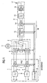
- FIG. 1 shows a transmission arrangement designed for continuous-time transmission Data transfer.
- This comprises a baseband signal processing unit 1, a quadrature modulator 2 and a radio frequency branch 3.
- the baseband signal processing unit 1 is designed for complex-valued signal processing and for this purpose comprises an in-phase branch 4 and a quadrature signal path 5.
- In-phase and quadrature signal paths 4, 5 are respectively designed to transmit symmetrical signals.
- inphase and quadrature signal paths 4, 5 each have a low-pass filter 6, each with a first programmable amplifier 7 is connected downstream.
- the first programmable amplifier 7 each have a control input for supplying a discrete-value control signal to the output of a Control unit 8 via a digital Dreileiterbus according to the 3Wire bus specification is connected.
- the quadrature modulator 2 comprises two Gilbert multipliers 9, with their first input pair with one output each of a first programmable Amplifier 7 are connected and their second input pair via a 0 degree / 90 degree frequency divider 10 to a voltage controlled Oscillator 11 for providing a complex-valued Signal connected to a carrier frequency is.
- the outputs of the two Gilbert multipliers 9 are on depending on an input pair of a summing node 12 connected, whose output forms the output of the quadrature modulator 2.
- the high frequency branch 3 connected, which is a passive, programmable Amplifier 13, a second programmable amplifier 14, a bandpass filter 15 and a power amplifier 16 includes.
- the power amplifier 16 has an output, the same time forms the output of the high-frequency branch 3 and which is coupled to an antenna 17.
- the passive, programmable Amplifier 13 is symmetrical with its input to the trained output of the summing node 12 connected.
- the output of the passive, programmable amplifier 13 is connected to the input of the second programmable Amplifier 14, which is an active amplifier connected.
- a bandpass filter 15 is connected.
- the output of the bandpass filter 15 is connected to an input of the power amplifier 16 coupled.
- Both the passive, programmable amplifier 13, as well as the second programmable amplifier 14 are to their Control with the control unit 8 via the three-wire bus connected.
- the described transmission arrangement for continuous-time data transmission is therefore as a homodyne transmitter or direct converter educated.
- the control of the programmable amplifier 7, 13, 14th by the control unit 8 by means of discrete-value signals.
- the transmission arrangement is for a continuous time Data transmission according to CDMA designed and as a UMTS transmitter educated. In such mobile devices according to UMTS standard is usually in addition to the shown transmission branch in addition a reception branch not shown in FIG Forming a transceiver provided.
- the total, controllable amplification of the transmission arrangement is for Achieve a large dynamic range on two active, programmable Amplifier stages 7, 14 and a passive, programmable Amplifier stage 13 distributed. It is in the Baseband signal processing unit 1 a gain control in the range of about 20 to 30 dB, while in the high-frequency branch 3 a dynamic range of about 50 to 60 dB as Control range is provided. Because at the output of the quadrature modulator advantageously a power level of about -10 dBm must be at the output of the quadrature modulator 2, a gain control range of about +15 to -45 be provided dB.
- a passive, programmable gain stage 13 which in the present embodiment as a controllable resistor network is executed.
- the passive programmable amplifier 13 and the second programmable amplifier 14 in steps adjustable by 6 dB.
- the first programmable amplifier 7 in baseband is adjustable in discrete steps of 1 dB.
- the amplification factors of the amplifiers 7, 13, 14 are thus not, as is usual with continuous data transmission systems provided, value-continuous, but value-discreet adjustable.
- Baseband and high frequency gain control can be total a resolution of the gain control of 1 dB by suitable control amplifier 7, 13, 14 by means of the control unit 8 and discrete-value control signals are achieved.
- the transmission arrangement according to the described embodiment is both in mobile radio systems of the second mobile generation with CDMA, the third generation and also in coming Generations of mobile systems, such as the planned fourth generation.
- FIG. 2 shows a development of the transmission arrangement of FIG 1 with an additional device for carrier frequency suppression 18, the output of the quadrature modulator. 2 coupled with its quadrature inputs. Apart from this Further development corresponds to the transmission arrangement of Figure 2 in their used components, their interconnection, their Functions and the advantageous interaction of the components the transmission arrangement of Figure 1, whose description is therefore to this point is not repeated.
- the additional loop for carrier frequency rejection comprises a feedback path containing the means for carrier frequency rejection 18 and that with its symmetrical trained input to the output of the summing node 12th connected.
- the carrier suppression means 18 two output terminal pairs are provided, the each with the inputs of the Gilbert mixer 9 at the symmetrical Coupled input pairs, such as shown in Figure 2 by means of adding nodes, which to another Inputs with the outputs of the programmable amplifier 7 are connected.
- the means for carrier frequency suppression 18 detects, if necessary translucent at the output of the quadrature modulator 2 Proportions of the carrier frequency provided by the VCO 11, English Carrier Frequency, and influences in theirs Dependence the in-phase and quadrature components of the baseband signals in the signal paths 4 and 5.
- an additional DC offset within the symmetry components of inphase branch 4 or inside the symmetry components of quadrature branch 5 or both be introduced.
- a carrier frequency rejection loop is especially in combination with the programmable amplifiers 7 advantageous, which may be reinforced Occurrence of frequency components at the carrier frequency on Output of the quadrature modulator 2 can lead.
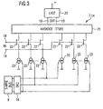
- FIG. 3 shows by way of example the structure of a programmable Amplifier with a variety of independently zuund switchable amplifier branches, the first and / or second programmable amplifier 7, 14 in the transmission arrangements can be used advantageously according to Figures 1 and 2.
- the programmable amplifier according to FIG 3 which is constructed in symmetrical circuit technology, a signal input 18 and a signal output 19 to which a electrical load 20 is connected.
- the amplifier includes three parallel-connected, symmetrical amplifier branches, each of a series circuit of a cascode stage 21, a field effect transistor 22 and a power source 23 are formed.
- the transistors 22 are each in pairs assigned to each other and paired at their control inputs connected to the signal input 18.
- the current sources 23 are also in pairs assigned to each other and each have Control inputs for switching on and off of the power sources 23 in pairs independently, with the control unit 8 are coupled.
- the control unit 8 stops value-discrete, digital signal for gain control via a three-wire bus ready.
- 22, 23 can be provided as many amplifier branches
- 16 amplifier branch pairs 21, 22, 23 already explained at the beginning allows the shutdown for the current transmission power not required amplifier branches a significant power reduction of the transmission arrangement and thus when using the transmission arrangement in portable mobile devices a significantly longer battery life or Talk time.
Landscapes
- Transmitters (AREA)
Claims (5)
- Dispositif d'émission pour la transmission de données en continu dans le temps, comprenant :une unité (1) de traitement de signal en bande de base conçue pour le traitement à valeur complexe d'un signal utile à émettre, ayant un chemin (4) de signal en phase et un chemin (5) de signal en quadrature,un modulateur (2) en quadrature comprenant une première entrée qui est couplée au chemin (4) de signal en phase, une deuxième entrée qui est couplée au chemin (5) de signal en quadrature et une sortie,une branche (3) de haute fréquence, qui est couplée à la sortie du modulateur (2) en quadrature,une unité (8) de commande, qui met à disposition un signal de commande de valeur discrète pour influer sur la puissance d'émission du dispositif d'émission,un premier amplificateur (7) programmable qui est disposé dans l'unité (1) de traitement de signal en bande de base pour amplifier le signal utile à émettre d'un facteur d'amplification réglable, ayant une entrée de commande qui est couplée à l'unité (8) de commande pour la transmission du signal de commande à valeur discrète, comprenant un sous-amplificateur disposé dans le chemin (4) du signal en phase et un sous-amplificateur disposé dans le chemin (5) du signal en quadrature,un deuxième amplificateur (14) programmable qui est disposé dans la branche (3) haute fréquence, comprenant une entrée de commande qui est couplée à l'unité (8) de commande pour la transmission d'un signal de commande à valeur discrète, etun chemin de couplage en retour, comprenant un moyen de suppression (18) de la fréquence porteuse, ayant une entrée qui est couplée à la sortie du modulateur (2) en quadrature et une sortie qui est couplée au chemin (4) de signal en phase et au chemin (5) de signal en quadrature.
- Dispositif d'émission suivant la revendication 1,
caractérisé en ce qu'il est prévu, dans l'unité (1) de traitement du signal en bande de base ou dans la branche (3) en haute fréquence, un amplificateur (13) programmable passif de traitement du signal utile à émettre, ayant une entrée de commande, qui est couplée à l'unité (8) de commande pour mettre à disposition une atténuation du signal à valeur discrète. - Dispositif d'émission suivant la revendication 1 ou 2,
caractérisé en ce que le premier et/ou le deuxième amplificateur (7, 14) programmable comprend plusieurs branches (21, 22, 23) d'amplificateur montées en parallèle et pouvant être branchées et débranchées indépendamment les unes des autres, le branchement et le débranchement des branches (21, 22, 23) d'amplificateur s'effectuant en fonction du signal de commande à valeur discrète. - Dispositif d'émission suivant l'une des revendications 1 à 3,
caractérisé en ce que le deuxième amplificateur (14) programmable comporte un moyen de réglage de la durée de montée du facteur d'amplification. - Dispositif d'émission suivant l'une des revendications 1 à 4,
caractérisé en ce que le dispositif d'émission est un émetteur téléphonique de téléphonie mobile.
Applications Claiming Priority (3)
| Application Number | Priority Date | Filing Date | Title |
|---|---|---|---|
| DE10163466 | 2001-12-21 | ||
| DE10163466A DE10163466A1 (de) | 2001-12-21 | 2001-12-21 | Sendeanordnung für zeitkontinuierliche Datenübertragung |
| PCT/DE2002/004624 WO2003056739A2 (fr) | 2001-12-21 | 2002-12-17 | Ensemble emetteur permettant la transmission de donnees en continu |
Publications (2)
| Publication Number | Publication Date |
|---|---|
| EP1456992A2 EP1456992A2 (fr) | 2004-09-15 |
| EP1456992B1 true EP1456992B1 (fr) | 2005-05-04 |
Family
ID=7710508
Family Applications (1)
| Application Number | Title | Priority Date | Filing Date |
|---|---|---|---|
| EP02792669A Expired - Lifetime EP1456992B1 (fr) | 2001-12-21 | 2002-12-17 | Ensemble emetteur permettant la transmission de donnees en continu |
Country Status (5)
| Country | Link |
|---|---|
| US (1) | US7555272B2 (fr) |
| EP (1) | EP1456992B1 (fr) |
| JP (1) | JP3970845B2 (fr) |
| DE (2) | DE10163466A1 (fr) |
| WO (1) | WO2003056739A2 (fr) |
Families Citing this family (13)
| Publication number | Priority date | Publication date | Assignee | Title |
|---|---|---|---|---|
| TWI260896B (en) * | 2003-04-04 | 2006-08-21 | Mediatek Inc | Wireless communication system with the device that detect transmission mode of communication signal |
| DE602004008769T2 (de) * | 2003-05-09 | 2008-01-24 | Nxp B.V. | Verfahren und Anordnung zur Einstellung der Sendeleistung eines Mobilübertragungsgerätes |
| DE10361651B4 (de) * | 2003-12-30 | 2013-12-05 | Intel Mobile Communications GmbH | Verfahren zum Kalibrieren einer Verstärkeranordnung |
| DE102004024875B4 (de) * | 2004-05-19 | 2006-09-07 | Infineon Technologies Ag | Verstärkeranordnung und Verfahren zur Kompensation eines Signalanteils in einer Verstärkeranordnung |
| US7664520B2 (en) | 2004-06-24 | 2010-02-16 | Nokia Corporation | Low current direct conversion transmitter architecture |
| DE102004039830B4 (de) * | 2004-08-17 | 2007-11-08 | Infineon Technologies Ag | Verstärkerschaltung mit einstellbarer wertdiskreter Verstärkung, Verwendung der Verstärkerschaltung und Verfahren zum Betreiben eines wertdiskret einstellbaren Verstärkers |
| DE102004059985B4 (de) * | 2004-12-13 | 2017-11-16 | Intel Deutschland Gmbh | Funksender mit einstellbaren Verstäkereinheiten im Basisband- und im Hochfrequenzabschnitt des Sendepfads |
| US7596185B2 (en) | 2004-12-13 | 2009-09-29 | Infineon Technologies Ag | Radio transmitter with variable amplifier units in the baseband section and in the radio-frequency section of the transmission path |
| JP4752272B2 (ja) * | 2005-01-05 | 2011-08-17 | ソニー株式会社 | 通信装置 |
| JP5195427B2 (ja) * | 2006-08-08 | 2013-05-08 | 日本電気株式会社 | 信号処理回路および信号処理方法 |
| US8315581B2 (en) | 2008-09-18 | 2012-11-20 | Intel Mobile Communications GmbH | Transmitter with hybrid closed loop power control |
| JP5564111B2 (ja) * | 2010-06-22 | 2014-07-30 | ルネサスエレクトロニクス株式会社 | 半導体装置 |
| JP7176403B2 (ja) * | 2018-12-26 | 2022-11-22 | 東ソー株式会社 | ラテックス接着剤組成物 |
Family Cites Families (16)
| Publication number | Priority date | Publication date | Assignee | Title |
|---|---|---|---|---|
| US5029233A (en) * | 1987-10-09 | 1991-07-02 | Motorola, Inc. | Radio arrangement having two radios sharing circuitry |
| US5066923A (en) * | 1990-10-31 | 1991-11-19 | Motorola, Inc. | Linear transmitter training method and apparatus |
| US5307512A (en) * | 1991-06-03 | 1994-04-26 | Motorola, Inc. | Power control circuitry for achieving wide dynamic range in a transmitter |
| US5333175A (en) * | 1993-01-28 | 1994-07-26 | Bell Communications Research, Inc. | Method and apparatus for dynamic power control in TDMA portable radio systems |
| JPH06303145A (ja) | 1993-04-13 | 1994-10-28 | Fujitsu Ltd | キャリアリーク抑圧回路 |
| GB2297443B (en) * | 1995-01-26 | 1999-09-08 | Sony Uk Ltd | Amplifier |
| JPH098578A (ja) | 1995-06-16 | 1997-01-10 | Sony Corp | 高周波用ステップアッテネータ |
| US5872481A (en) | 1995-12-27 | 1999-02-16 | Qualcomm Incorporated | Efficient parallel-stage power amplifier |
| JP3231992B2 (ja) | 1996-02-20 | 2001-11-26 | モトローラ株式会社 | 送信装置 |
| US5745480A (en) * | 1996-04-03 | 1998-04-28 | Adicom Wireless, Inc. | Multi-rate wireless communications system |
| US5708681A (en) * | 1996-04-23 | 1998-01-13 | Bell Communications Research, Inc. | Hybrid analog/digital method and apparatus for controlling the transmission power level of a radio transceiver |
| US6466628B1 (en) | 1998-04-18 | 2002-10-15 | Lucent Technologies Inc. | Technique for effectively rendering power amplification and control in wireless communications |
| FI105612B (fi) * | 1998-10-23 | 2000-09-15 | Nokia Networks Oy | Menetelmä ja kytkentä vaihevirheen korjaamiseksi tehovahvistimen linearisointisilmukassa |
| US6370203B1 (en) | 1998-11-04 | 2002-04-09 | Ericsson Inc. | Power control for wireless communications system |
| WO2002084935A1 (fr) * | 2001-04-17 | 2002-10-24 | Nokia Corporation | Procedes pour determiner les gains de differentes porteuses, unites de radiotransmission et modules pour ces unites |
| US7164893B2 (en) * | 2001-08-31 | 2007-01-16 | Motorola, Inc. | Method and apparatus for optimizing supply modulation in a transmitter |
-
2001
- 2001-12-21 DE DE10163466A patent/DE10163466A1/de not_active Ceased
-
2002
- 2002-12-17 EP EP02792669A patent/EP1456992B1/fr not_active Expired - Lifetime
- 2002-12-17 JP JP2003557131A patent/JP3970845B2/ja not_active Expired - Fee Related
- 2002-12-17 WO PCT/DE2002/004624 patent/WO2003056739A2/fr not_active Ceased
- 2002-12-17 DE DE50203038T patent/DE50203038D1/de not_active Expired - Lifetime
-
2004
- 2004-06-21 US US10/872,815 patent/US7555272B2/en active Active
Also Published As
| Publication number | Publication date |
|---|---|
| WO2003056739A3 (fr) | 2004-02-26 |
| US20050032489A1 (en) | 2005-02-10 |
| DE10163466A1 (de) | 2003-07-10 |
| JP2005513952A (ja) | 2005-05-12 |
| WO2003056739A2 (fr) | 2003-07-10 |
| US7555272B2 (en) | 2009-06-30 |
| JP3970845B2 (ja) | 2007-09-05 |
| DE50203038D1 (de) | 2005-06-09 |
| EP1456992A2 (fr) | 2004-09-15 |
Similar Documents
| Publication | Publication Date | Title |
|---|---|---|
| DE4193233C2 (de) | Einrichtung und Verfahren zur Gleichstromversatz-Korrektur für einen Empfänger | |
| DE69120891T2 (de) | Leistungsverstärker und mobiles Funkgerät mit einem derartigen Verstärker | |
| DE4291712C1 (de) | Vorrichtung zur Steuerung der Sendeleistung bei einem CDMA-Funkgerät | |
| DE69024096T2 (de) | Schaltung zur Bildung niedriger Leistungspegel in einem Funktelefonsender | |
| EP1211801B1 (fr) | Emetteur utilisant une boucle polaire | |
| DE4291711C2 (de) | Leistungssteuerschaltkreis sowie Verfahren zum Einstellen des Leistungspegels eines Funkfrequenzsignals | |
| DE69727962T2 (de) | Effizienter leistungsverstärker mit parallelen stufen | |
| EP0797312A2 (fr) | Commutateur pour commuter entre réception et émission avec des semi-conducteurs | |
| DE19713101A1 (de) | Mehrstufige Verstaerkerschaltung mit veraenderlicher Verstaerkung | |
| DE102016103666A1 (de) | Vorrichtung mit einer schalteinheit und anwendungen davon | |
| DE10163466A1 (de) | Sendeanordnung für zeitkontinuierliche Datenübertragung | |
| DE4409382C2 (de) | Sendeempfangsgerät | |
| EP0654900B1 (fr) | Appareil de radiocommunication avec commande de puissance d'émission | |
| DE102012006889A1 (de) | Mischerschaltung | |
| EP1407543B1 (fr) | Dispositif d'emission a regulation de puissance | |
| WO2003005582A2 (fr) | Circuit multiplicateur | |
| DE102005008372B4 (de) | Steuerbarer Verstärker und dessen Verwendung | |
| DE102005030349B4 (de) | Empfangsvorrichtung und Verfahren zum Anpassen eines Dynamikbereichs einer Empfangsvorrichtung | |
| DE69829036T2 (de) | Verbesserter linearer vorwärtsgekoppelter Hochfrequenz-Mehrträger-Leistungsverstärker | |
| DE102009029422B4 (de) | Sender mit Hybrid-Leistungsregelung | |
| DE60300716T2 (de) | Funksender | |
| DE102006004227B4 (de) | Verstärkeranordnung mit variablem Verstärkungsfaktor | |
| EP1382111B1 (fr) | Recepteur haute frequence | |
| EP0597534A2 (fr) | Emetteur-récepteur radio | |
| DE102006043902B4 (de) | Stromwandler, Frequenzmischer und Verfahren zur Frequenzmischung |
Legal Events
| Date | Code | Title | Description |
|---|---|---|---|
| PUAI | Public reference made under article 153(3) epc to a published international application that has entered the european phase |
Free format text: ORIGINAL CODE: 0009012 |
|
| 17P | Request for examination filed |
Effective date: 20040629 |
|
| AK | Designated contracting states |
Kind code of ref document: A2 Designated state(s): AT BE BG CH CY CZ DE DK EE ES FI FR GB GR IE IT LI LU MC NL PT SE SI SK TR |
|
| GRAP | Despatch of communication of intention to grant a patent |
Free format text: ORIGINAL CODE: EPIDOSNIGR1 |
|
| RIC1 | Information provided on ipc code assigned before grant |
Ipc: 7H 03G 3/30 B Ipc: 7H 04L 1/00 A |
|
| GRAS | Grant fee paid |
Free format text: ORIGINAL CODE: EPIDOSNIGR3 |
|
| GRAA | (expected) grant |
Free format text: ORIGINAL CODE: 0009210 |
|
| AK | Designated contracting states |
Kind code of ref document: B1 Designated state(s): DE FR GB |
|
| PG25 | Lapsed in a contracting state [announced via postgrant information from national office to epo] |
Ref country code: GB Free format text: LAPSE BECAUSE OF FAILURE TO SUBMIT A TRANSLATION OF THE DESCRIPTION OR TO PAY THE FEE WITHIN THE PRESCRIBED TIME-LIMIT Effective date: 20050504 |
|
| REG | Reference to a national code |
Ref country code: GB Ref legal event code: FG4D Free format text: NOT ENGLISH |
|
| REG | Reference to a national code |
Ref country code: IE Ref legal event code: FG4D Free format text: LANGUAGE OF EP DOCUMENT: GERMAN |
|
| REF | Corresponds to: |
Ref document number: 50203038 Country of ref document: DE Date of ref document: 20050609 Kind code of ref document: P |
|
| GBV | Gb: ep patent (uk) treated as always having been void in accordance with gb section 77(7)/1977 [no translation filed] |
Effective date: 20050504 |
|
| PLBE | No opposition filed within time limit |
Free format text: ORIGINAL CODE: 0009261 |
|
| STAA | Information on the status of an ep patent application or granted ep patent |
Free format text: STATUS: NO OPPOSITION FILED WITHIN TIME LIMIT |
|
| 26N | No opposition filed |
Effective date: 20060207 |
|
| EN | Fr: translation not filed | ||
| PG25 | Lapsed in a contracting state [announced via postgrant information from national office to epo] |
Ref country code: FR Free format text: LAPSE BECAUSE OF NON-PAYMENT OF DUE FEES Effective date: 20051231 |
|
| PG25 | Lapsed in a contracting state [announced via postgrant information from national office to epo] |
Ref country code: FR Free format text: LAPSE BECAUSE OF NON-PAYMENT OF DUE FEES Effective date: 20050504 |
|
| REG | Reference to a national code |
Ref country code: DE Ref legal event code: R081 Ref document number: 50203038 Country of ref document: DE Owner name: INTEL MOBILE COMMUNICATIONS GMBH, DE Free format text: FORMER OWNER: INFINEON TECHNOLOGIES AG, 81669 MUENCHEN, DE Effective date: 20130314 Ref country code: DE Ref legal event code: R081 Ref document number: 50203038 Country of ref document: DE Owner name: INTEL MOBILE COMMUNICATIONS GMBH, DE Free format text: FORMER OWNER: INTEL MOBILE COMMUNICATIONS TECHNOLOGY GMBH, 85579 NEUBIBERG, DE Effective date: 20130326 Ref country code: DE Ref legal event code: R081 Ref document number: 50203038 Country of ref document: DE Owner name: INTEL MOBILE COMMUNICATIONS GMBH, DE Free format text: FORMER OWNER: INTEL MOBILE COMMUNICATIONS GMBH, 85579 NEUBIBERG, DE Effective date: 20130315 Ref country code: DE Ref legal event code: R081 Ref document number: 50203038 Country of ref document: DE Owner name: INTEL MOBILE COMMUNICATIONS GMBH, DE Free format text: FORMER OWNER: INFINEON TECHNOLOGIES AG, 85579 NEUBIBERG, DE Effective date: 20130315 |
|
| PGFP | Annual fee paid to national office [announced via postgrant information from national office to epo] |
Ref country code: DE Payment date: 20171212 Year of fee payment: 16 |
|
| REG | Reference to a national code |
Ref country code: DE Ref legal event code: R119 Ref document number: 50203038 Country of ref document: DE |
|
| PG25 | Lapsed in a contracting state [announced via postgrant information from national office to epo] |
Ref country code: DE Free format text: LAPSE BECAUSE OF NON-PAYMENT OF DUE FEES Effective date: 20190702 |