EP1458018B1 - Elektronisches Bauelement und Verfahren zu seiner Herstellung - Google Patents
Elektronisches Bauelement und Verfahren zu seiner Herstellung Download PDFInfo
- Publication number
- EP1458018B1 EP1458018B1 EP04001572A EP04001572A EP1458018B1 EP 1458018 B1 EP1458018 B1 EP 1458018B1 EP 04001572 A EP04001572 A EP 04001572A EP 04001572 A EP04001572 A EP 04001572A EP 1458018 B1 EP1458018 B1 EP 1458018B1
- Authority
- EP
- European Patent Office
- Prior art keywords
- wiring lines
- board
- electronic component
- ultrasonic vibration
- wiring
- Prior art date
- Legal status (The legal status is an assumption and is not a legal conclusion. Google has not performed a legal analysis and makes no representation as to the accuracy of the status listed.)
- Expired - Lifetime
Links
Images




Classifications
-
- F—MECHANICAL ENGINEERING; LIGHTING; HEATING; WEAPONS; BLASTING
- F04—POSITIVE - DISPLACEMENT MACHINES FOR LIQUIDS; PUMPS FOR LIQUIDS OR ELASTIC FLUIDS
- F04B—POSITIVE-DISPLACEMENT MACHINES FOR LIQUIDS; PUMPS
- F04B39/00—Component parts, details, or accessories, of pumps or pumping systems specially adapted for elastic fluids, not otherwise provided for in, or of interest apart from, groups F04B25/00 - F04B37/00
- F04B39/10—Adaptations or arrangements of distribution members
- F04B39/1066—Valve plates
-
- H—ELECTRICITY
- H05—ELECTRIC TECHNIQUES NOT OTHERWISE PROVIDED FOR
- H05K—PRINTED CIRCUITS; CASINGS OR CONSTRUCTIONAL DETAILS OF ELECTRIC APPARATUS; MANUFACTURE OF ASSEMBLAGES OF ELECTRICAL COMPONENTS
- H05K1/00—Printed circuits
- H05K1/02—Details
- H05K1/0271—Arrangements for reducing stress or warp in rigid printed circuit boards, e.g. caused by loads, vibrations or differences in thermal expansion
-
- F—MECHANICAL ENGINEERING; LIGHTING; HEATING; WEAPONS; BLASTING
- F04—POSITIVE - DISPLACEMENT MACHINES FOR LIQUIDS; PUMPS FOR LIQUIDS OR ELASTIC FLUIDS
- F04B—POSITIVE-DISPLACEMENT MACHINES FOR LIQUIDS; PUMPS
- F04B39/00—Component parts, details, or accessories, of pumps or pumping systems specially adapted for elastic fluids, not otherwise provided for in, or of interest apart from, groups F04B25/00 - F04B37/00
- F04B39/0027—Pulsation and noise damping means
-
- H—ELECTRICITY
- H05—ELECTRIC TECHNIQUES NOT OTHERWISE PROVIDED FOR
- H05K—PRINTED CIRCUITS; CASINGS OR CONSTRUCTIONAL DETAILS OF ELECTRIC APPARATUS; MANUFACTURE OF ASSEMBLAGES OF ELECTRICAL COMPONENTS
- H05K2201/00—Indexing scheme relating to printed circuits covered by H05K1/00
- H05K2201/10—Details of components or other objects attached to or integrated in a printed circuit board
- H05K2201/10227—Other objects, e.g. metallic pieces
- H05K2201/10416—Metallic blocks or heatsinks completely inserted in a PCB
-
- H—ELECTRICITY
- H05—ELECTRIC TECHNIQUES NOT OTHERWISE PROVIDED FOR
- H05K—PRINTED CIRCUITS; CASINGS OR CONSTRUCTIONAL DETAILS OF ELECTRIC APPARATUS; MANUFACTURE OF ASSEMBLAGES OF ELECTRICAL COMPONENTS
- H05K2201/00—Indexing scheme relating to printed circuits covered by H05K1/00
- H05K2201/10—Details of components or other objects attached to or integrated in a printed circuit board
- H05K2201/10613—Details of electrical connections of non-printed components, e.g. special leads
- H05K2201/10621—Components characterised by their electrical contacts
- H05K2201/10674—Flip chip
-
- H—ELECTRICITY
- H05—ELECTRIC TECHNIQUES NOT OTHERWISE PROVIDED FOR
- H05K—PRINTED CIRCUITS; CASINGS OR CONSTRUCTIONAL DETAILS OF ELECTRIC APPARATUS; MANUFACTURE OF ASSEMBLAGES OF ELECTRICAL COMPONENTS
- H05K2201/00—Indexing scheme relating to printed circuits covered by H05K1/00
- H05K2201/20—Details of printed circuits not provided for in H05K2201/01 - H05K2201/10
- H05K2201/2009—Reinforced areas, e.g. for a specific part of a flexible printed circuit
-
- H—ELECTRICITY
- H05—ELECTRIC TECHNIQUES NOT OTHERWISE PROVIDED FOR
- H05K—PRINTED CIRCUITS; CASINGS OR CONSTRUCTIONAL DETAILS OF ELECTRIC APPARATUS; MANUFACTURE OF ASSEMBLAGES OF ELECTRICAL COMPONENTS
- H05K2201/00—Indexing scheme relating to printed circuits covered by H05K1/00
- H05K2201/20—Details of printed circuits not provided for in H05K2201/01 - H05K2201/10
- H05K2201/2045—Protection against vibrations
-
- H—ELECTRICITY
- H05—ELECTRIC TECHNIQUES NOT OTHERWISE PROVIDED FOR
- H05K—PRINTED CIRCUITS; CASINGS OR CONSTRUCTIONAL DETAILS OF ELECTRIC APPARATUS; MANUFACTURE OF ASSEMBLAGES OF ELECTRICAL COMPONENTS
- H05K2203/00—Indexing scheme relating to apparatus or processes for manufacturing printed circuits covered by H05K3/00
- H05K2203/02—Details related to mechanical or acoustic processing, e.g. drilling, punching, cutting, using ultrasound
- H05K2203/0285—Using ultrasound, e.g. for cleaning, soldering or wet treatment
-
- H—ELECTRICITY
- H05—ELECTRIC TECHNIQUES NOT OTHERWISE PROVIDED FOR
- H05K—PRINTED CIRCUITS; CASINGS OR CONSTRUCTIONAL DETAILS OF ELECTRIC APPARATUS; MANUFACTURE OF ASSEMBLAGES OF ELECTRICAL COMPONENTS
- H05K3/00—Apparatus or processes for manufacturing printed circuits
- H05K3/30—Assembling printed circuits with electric components, e.g. with resistors
- H05K3/32—Assembling printed circuits with electric components, e.g. with resistors electrically connecting electric components or wires to printed circuits
- H05K3/328—Assembling printed circuits with electric components, e.g. with resistors electrically connecting electric components or wires to printed circuits by welding
-
- H—ELECTRICITY
- H10—SEMICONDUCTOR DEVICES; ELECTRIC SOLID-STATE DEVICES NOT OTHERWISE PROVIDED FOR
- H10W—GENERIC PACKAGES, INTERCONNECTIONS, CONNECTORS OR OTHER CONSTRUCTIONAL DETAILS OF DEVICES COVERED BY CLASS H10
- H10W72/00—Interconnections or connectors in packages
- H10W72/071—Connecting or disconnecting
- H10W72/072—Connecting or disconnecting of bump connectors
- H10W72/07231—Techniques
- H10W72/07232—Compression bonding, e.g. thermocompression bonding
- H10W72/07233—Ultrasonic bonding, e.g. thermosonic bonding
-
- H—ELECTRICITY
- H10—SEMICONDUCTOR DEVICES; ELECTRIC SOLID-STATE DEVICES NOT OTHERWISE PROVIDED FOR
- H10W—GENERIC PACKAGES, INTERCONNECTIONS, CONNECTORS OR OTHER CONSTRUCTIONAL DETAILS OF DEVICES COVERED BY CLASS H10
- H10W72/00—Interconnections or connectors in packages
- H10W72/071—Connecting or disconnecting
- H10W72/072—Connecting or disconnecting of bump connectors
- H10W72/07231—Techniques
- H10W72/07236—Soldering or alloying
-
- H—ELECTRICITY
- H10—SEMICONDUCTOR DEVICES; ELECTRIC SOLID-STATE DEVICES NOT OTHERWISE PROVIDED FOR
- H10W—GENERIC PACKAGES, INTERCONNECTIONS, CONNECTORS OR OTHER CONSTRUCTIONAL DETAILS OF DEVICES COVERED BY CLASS H10
- H10W72/00—Interconnections or connectors in packages
- H10W72/90—Bond pads, in general
-
- H—ELECTRICITY
- H10—SEMICONDUCTOR DEVICES; ELECTRIC SOLID-STATE DEVICES NOT OTHERWISE PROVIDED FOR
- H10W—GENERIC PACKAGES, INTERCONNECTIONS, CONNECTORS OR OTHER CONSTRUCTIONAL DETAILS OF DEVICES COVERED BY CLASS H10
- H10W72/00—Interconnections or connectors in packages
- H10W72/90—Bond pads, in general
- H10W72/941—Dispositions of bond pads
- H10W72/9415—Dispositions of bond pads relative to the surface, e.g. recessed, protruding
-
- H—ELECTRICITY
- H10—SEMICONDUCTOR DEVICES; ELECTRIC SOLID-STATE DEVICES NOT OTHERWISE PROVIDED FOR
- H10W—GENERIC PACKAGES, INTERCONNECTIONS, CONNECTORS OR OTHER CONSTRUCTIONAL DETAILS OF DEVICES COVERED BY CLASS H10
- H10W90/00—Package configurations
- H10W90/701—Package configurations characterised by the relative positions of pads or connectors relative to package parts
- H10W90/721—Package configurations characterised by the relative positions of pads or connectors relative to package parts of bump connectors
- H10W90/724—Package configurations characterised by the relative positions of pads or connectors relative to package parts of bump connectors between a chip and a stacked insulating package substrate, interposer or RDL
Definitions
- the present invention relates to an electronic component device formed by mounting an electronic component on a board via bumps, and more specifically, the present invention relates to an electronic component device implemented by using a flip chip bonding method.
- Japanese Unexamined Patent Application Publication No. 63-288031 discloses a flip chip bonding method in which bumps formed on respective electrodes of a semiconductor chip are aligned with respective wiring patterns on a board disposed on a heated stage, and in which pressure and ultrasonic vibration are applied to the rear surface of the chip via a tool, thereby bonding the bumps and the respective wiring patterns together.
- Fig. 1 shows an example of an electronic component device.
- Fig. 2 illustrates a bonding method for this electronic component device.
- Fig. 3 shows a board of the electronic component device.
- reference numeral 1 denotes a board
- 2a and 2b each denote a wiring line
- 3 denotes a bump
- 4 denotes an electronic component.
- the wiring lines 2a and 2b are longitudinally and laterally arranged on the board 1, and the bumps 3 are formed in advance on respective electrodes (not shown) of the electronic component 4.
- the top surface of the electronic component 4 is pressed by a bonding tool 5 and is subjected to ultrasonic vibration U along a horizontal direction via the bonding tool 5, whereby the bumps 3 are bonded to the respective wiring lines 2a and 2b.
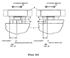
- the perpendicular wiring lines 2a exhibit a small deformation inhibiting effect as compared with the parallel wiring lines 2b, which are arranged along the longitudinal direction with respect to the ultrasonic vibration, so that the perpendicular wiring lines 2a are displaced more than the parallel wiring lines 2b, as shown in Figs. 4A and 4B (here, reference numeral 6 denotes an electrode of the electronic component 4, and a symbol ⁇ denotes a displacement).
- Table 1 shows analysis results using a finite-element method, on a displacement of the wiring line and that of the board surface when a forced displacement of 1 ⁇ m is statically applied to the chip surface as ultrasonic vibration.
- TABLE 1 Parallel wiring line Perpendicular wiring line A Displacement of wiring line [ ⁇ m] 0. 66 0. 75 B Displacement of board surface [ ⁇ m] 0. 48 0. 55 Deformation amount of wiring line (A-B) 0. 18 0. 20 Deformation amount of board (equal to B) 0. 48 0. 55
- the perpendicular wiring line exhibits a larger displacement than the parallel wiring line. While ultrasonic vibration is applied, displacements repeatedly occur, thereby causing a difference in bondability between the perpendicular wiring line and the parallel wiring line.
- Fig. 5 shows the relationship between the displacement of wiring line and the bonding strength. As can be seen from Fig. 5, the larger the displacement, the smaller the bonding strength.
- Japanese Unexamined Patent Application Publication No. 2002-184812 proposes that, in order to make displacements of wiring lines due to ultrasonic vibration substantially uniform, the connecting section of each of the wiring lines of which the angle ⁇ with respect to a direction of ultrasonic vibration is larger, was formed wider than the connecting section of each of the wiring lines of which the angle ⁇ with respect to the direction of ultrasonic vibration is smaller, thereby bringing all wiring lines into a substantially uniform bonding state. More specifically, the width of each of the perpendicular wiring lines was made wider than that of each of the parallel wiring lines.
- each of the perpendicular wiring lines must be formed wider and, therefore, if wiring lines are arranged at a high density, it is difficult to secure a sufficient formation width. This make it difficult to bring all wiring lines into a uniform bonding state.
- JP 2002164643 A relates to a flip-chip bonding structure in which a semiconductor integrated circuit chip is mounted directly on a first surface of a flexible printed circuit board. An opposite second surface of the flexible print circuit board is adhered to a metallic material by an adhesive tape. Below the position where the chip is mounted, the adhesive tape is substituted by a resin in order to obtain a stiffened structure.
- US-A-5,252,519 relates to a multilayered glass-ceramic substrate having electrodes for flip-chip mounting on an external surface and having internal wiring structures overlapping the external electrode.
- US-B-6,265,300 relates to a wire-bonding surface and a bonding method.
- a bonding pad structure for use with compliant dielectric materials and a method for wire bonding is described in which a rigid layer is formed between the bonding pad and the compliant dielectric layer.
- the rigid layer increases the stiffness of the bonding structure such that an effective bond may be achieved by conventional ultrasonic and thermosonic bonding methods.
- bumps are formed on electrodes of an electric component in advance, and these bumps are bonded, using ultrasonic vibration, to respective wiring lines on a board, which face the respective bumps.
- wiring lines of which the angle ⁇ 1 with respect to the direction of ultrasonic vibration is larger, and wiring lines of which the angle ⁇ 2 with respect to the direction of ultrasonic vibration is smaller, become mixed with each other.
- a displacement inhibiting layer having higher rigidity than the material of the board is provided inside the board in a portion below each of the wiring lines of which the angle ⁇ with respect to the direction of ultrasonic vibration is larger, it is possible to make displacements of the wiring lines due to ultrasonic vibration substantially uniform, and to bring all wiring lines into a substantially uniform bonding state irrespective of the magnitude relationship of the angle ⁇ . This inhibits the occurrence of imperfect bonding and cracking.
- the materials of board preferably include resin and ceramic materials.
- the ceramic material which has high rigidity, is low in displacement due to ultrasonic vibration.
- the board made of resin which experiences large displacements due to ultrasonic vibration, is subject to variations in bondability. Therefore, preferred embodiments of the present invention exert a larger effect when a resin board is used.
- first wiring lines extending substantially parallel to the direction of ultrasonic vibration and second wiring lines extending substantially perpendicular to the direction of the ultrasonic vibration be arranged on the board along the directions that are substantially perpendicular to each other, and that the displacement inhibiting layer be provided inside the board in a portion below each of the second wiring lines.
- the direction of ultrasonic vibration and that of wiring lines can be arbitrarily set.
- first wiring lines which extend substantially parallel to the direction of ultrasonic vibration
- second wiring lines which extend substantially perpendicularly to the direction of ultrasonic vibration
- the displacement inhibiting layer is preferably disposed in a portion below the plurality of the second wiring lines so as to be continuous.
- An alternative method for providing the displacement inhibiting layer is to form each of the displacement inhibiting layers in a portion below a respective one of the second wiring lines in an independent manner.
- providing the displacement inhibiting layer in a portion below a plurality of the second wiring lines so as to be continuous as described above allows even the displacement of a board portion situated between the second wiring lines to be inhibited by the displacement inhibiting layer, thereby increasing the displacement inhibiting effect with respect to the second wiring lines.
- the displacement inhibiting layer has only to be continuous with respect to at least two adjacent wiring lines.
- the displacement inhibiting layer be provided in a region within, for example, about 1 mm of the surface of the board.
- the displacement inhibiting layer be provided as close to the board surface having thereon the wiring line as possible.
- the displacement inhibiting layer is preferably provided in a region within, for example, about 1 mm of the board surface. The closer to the board surface, the more effective the displacement inhibiting layer. It is therefore more preferable that the displacement inhibiting layer be provided in a region within, for example, about 10 ⁇ m to about 150 ⁇ m of the board surface.
- the board may be a multilayer printed wiring board
- the displacement inhibiting layer may be a conductor pattern provided in an inner layer of the multilayer printed wiring board.
- a conductor pattern is provided in an inner layer thereof besides wiring patterns on outer layers of both sides of the board, and therefore, by using one of these conductor patterns as a displacement inhibiting layer, it is possible to easily form a displacement inhibiting layer without using a special technique, and also to provide the displacement inhibiting layer with a function as a ground or a shield.
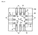
- FIG. 6 is a plan view of this electronic component device.
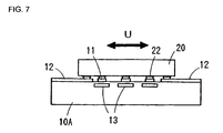
- Fig. 7 is a side view of the electronic component device.
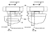
- Figs. 8A and 8B are each an enlarged sectional view of a bonding portion.
- a board 10A preferably includes an organic board made of a material such as glass epoxy resin or bismaleimide triazine (BT) resin, a ceramic board such as alumina, or a crystal board made of silicon or other suitable material.
- a plurality of wiring lines 11 and 12 that extend along directions that substantially perpendicularly intersect each other is formed on the board 10A. As shown in Fig. 6, each of the wiring lines 11 is arranged so as to form an angle ⁇ 1 with respect to a direction of ultrasonic vibration U (described below) that is larger than approximately 45° ( ⁇ 1 > 45°), and each of the wiring lines 12 is arranged to form an angle ⁇ 2 with respect to the direction of ultrasonic vibration U that is smaller than approximately ( ⁇ 2 ⁇ 45°). Thus, the angle ⁇ 1 is greater than the angle ⁇ 2
- each individual displacement inhibiting layer 13 is provided in a portion below a respective one of the substantially perpendicular wiring lines 11.
- the displacement inhibiting layers 13 are provided in a region corresponding to the electronic component mounting portion (indicated by a chain double-dashed line in Fig. 6), of the substantially perpendicular wiring lines 11, that is, in a region including land portions 11 a and 12a.
- a "portion below a wiring line” refers to, for example, "a region within about 1 mm of the surface of the board".
- the displacement inhibiting layer be arranged as close to the board surface as possible.
- the displacement inhibiting layer is provided in a region, for example, within about 10 ⁇ m to about 150 ⁇ m of the board surface.
- the material of the displacement inhibiting layer 13 is preferably a metallic material such as Cu, or a ceramic material, with high rigidity material, such as alumina, or other suitable material.
- An organic board preferably has a rigidity in a range of about 10 GPa to about 60 GPa, whereas a Cu material has rigidity of about 120 GPa or more, although the rigidity changes with temperature. Therefore, when an organic board is used as the board 10A, a Cu material can function effectively as the displacement inhibiting layer 13.
- the shape of the board 10A is not particularly limited.
- the thickness of the board 10A can also be arbitrarily set, for example, to be in a range of about 0.2 mm to about 2 mm.
- the wiring lines 11 and 12 are formed preferably by using a plating method, thin film forming method, or thick film forming method, or other suitable method.
- the thickness of the wiring line is preferably in a range of several micrometers to several tens of micrometers, but is not restricted to this range.
- the wiring lines 11 and 12 used were formed by applying electrolytic plating or electroless plating of Ni (approximately 3 ⁇ m thick) or Au (approximately 0.03 ⁇ m or more thick) to Cu foil with a thickness in a range of about 5 ⁇ m to about 35 ⁇ m.
- the widths of the wiring lines 11 and 12 are preferably made substantially the same. However, the widths as well as the shapes of the wiring lines 11 and 12 may be different from each other. Also, the arrangement may be such that the region corresponding to the electronic component mounting portion (the portion indicated by the chain double-dashed line in Fig. 6), of the wiring lines 11 and 12, that is, the region including the land portions 11 a and 12a, are exclusively exposed to the outside, and that the other region is covered with an insulating material such as resist.
- the electronic component 20 preferably is, for example, a semiconductor chip or a surface acoustic wave (SAW) device.
- electrode pads 21 (see Figs. 8A and 8B) preferably made of Al or AU material of, e.g., about 100 ⁇ m square are formed in positions corresponding to the land portions 11 a and 12a.
- Bumps 22 are formed on the respective electrode pads 21, preferably using a plating method, wire-bonding method, or vapor deposition method, or other suitable method. Au, Ag, Pd, Cu, Al, or solder, or other suitable material, is usable for the bumps 22.
- the bumps 22 are collectively bonded to the respective land portions 11a and 12a of the wiring lines 11 and 12 by applying, to the electronic component 20, ultrasonic vibration, a load, and further heat, if necessary.
- bumps 22 are formed on the respective electrode pads 21 of the electronic component 20.
- a bonding tool (not shown)
- the top surface (rear surface) of the electronic component 20 is attracted, and the electronic component 20 is picked up.
- the bumps 22 are aligned with the respective land portions 11 a and 12a of the wiring lines 11 and 12 of the board 10A, with a high degree of accuracy.
- the bumps 22 of the electronic component 20 and the respective land portions 11a and 12a of the wiring lines 11 and 12 of the board 10A are brought into contact.
- ultrasonic vibration U at a frequency in a range of, e.g., about 20 kHz to about 150 kHz is applied to the top surface of the electronic component 20 in the direction that is substantially parallel to the surface of the board 10A, and simultaneously in the direction that is substantially perpendicular to the substantially perpendicular wire lines 11 (i.e., in the direction that is substantially parallel to the parallel wiring lines 12) via the bonding tool, thereby bonding the bumps 22 and the respective land portions 11a and 12a together.
- a load may be applied between the board 10A and the electronic component 20, and either of the board 10A and the electronic component 20 may be heated.
- the gap between the electronic component 20 and the board 10A may be subjected to resin sealing to mitigate the difference in linear expansion between the electronic component 20 and the board 10A, and to protect the bonding portion.
- the resin sealing may be performed by applying resin after the bonding between the electronic component 20 and the board 10A.
- the resin sealing may be performed such that resin is applied to the wiring lines on the board in advance, and such that the bumps are bonded to the respective wiring lines on the board while breaking through the resin layer. In this case, bonding and resin sealing can be concurrently achieved.
- the substantially perpendicular wiring lines 11 When applying ultrasonic vibration U, the substantially perpendicular wiring lines 11 exhibit low rigidity with respect to the vibration direction compared with the substantially parallel wiring lines 12. However, since the substantially perpendicular wiring lines 11 each have a displacement inhibiting layer 13 formed therebelow, the difference in displacement between the substantially perpendicular wiring lines 11 and the substantially parallel wiring lines 12 decreases, as shown in Figs. 8A and 8B. As a result, the variation in the bondability with respect to the bumps 13 between the substantially perpendicular wiring lines 11 and the substantially parallel wiring lines 12 is reduced, and thereby substantially uniform bonding strength can be achieved. This prevents the occurrence of imperfect bonding and cracking in the electrodes.
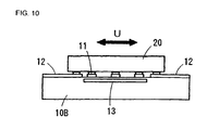
- Figs. 9 and 10 show an electronic component device according to a second preferred embodiment of the present invention.
- the same elements as those in Figs. 6 and 7 are denoted by the same reference numerals.
- a board 10B has thereon a plurality of wiring lines 11 and 12 that are formed along directions that substantially perpendicularly intersect each other.
- Displacement inhibiting layers 13 having higher rigidity than the board material are provided inside the board 10B in portions below the substantially perpendicular wiring lines 11.
- the displacement inhibiting layer 13 in this preferred embodiment is arranged so as to be continuous with respect to a plurality of substantially perpendicular wiring lines 11 (three in this case). More specifically, even portions situated between adjacent substantially perpendicular wiring lines 11 are provided with the displacement inhibiting layer 13.
- the portions of the board 10B that are situated between the substantially perpendicular wiring lines 11 are also prevented from being displaced because of the displacement inhibiting layer 13, the displacement of the substantially perpendicular wiring lines 11 and their peripheries due to ultrasonic vibration is reliably prevented. This further reduces the displacement difference from the substantially parallel wiring lines, resulting in more uniform bonding strength.
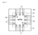
- Fig. 11 shows an electronic component device according to a third preferred embodiment of the present invention.
- the same elements as those in Figs. 6 and 7 are denoted by the same reference numerals.
- a board 10C in this preferred embodiment is arranged so that portions having no displacement inhibiting layer 13 are limited to portions below the substantially parallel wiring lines 12.
- displacement inhibiting layers 13 are provided over substantially the entire region inside the board 10C.
- window holes 13a are provided in portions of the displacement inhibiting layers 13, corresponding to the portions below the substantially parallel wiring lines 12.
- a printed wiring board having three layers or more of conductor patterns is referred to as a "multilayer printed wiring board".
- conductor patterns commonly Cu
- providing the conductor pattern in the inner layer having higher rigidity than the resin layer, as a displacement inhibiting layer allows the advantages of preferred embodiments of the present invention to be easily obtained without using a special technique.
- applying preferred embodiments of the present invention to commodity products including a multilayer printed wiring board allows the advantages of preferred embodiments of the present invention to be achieved without causing an increase in cost.
- the present invention is not limited to the above-described preferred embodiments.
- the bumps are preferably formed on the electronic component.
- wiring lines along the directions that are substantially perpendicular and substantially parallel to the direction of ultrasonic vibration are provided on the surface of the board.
- wiring lines may be provided along directions that are inclined with respect to the direction of ultrasonic vibration.
- the widths of the substantially perpendicular wiring line and the substantially parallel wiring line are preferably substantially equal.
- the width of the substantially perpendicular wiring line, which has a displacement inhibiting layer may be wider than that of the substantially parallel wiring line. This offers the advantage of increasing flexibility in the design of the widths of the displacement inhibiting layer and the substantially perpendicular wiring line.
- the material of the board is not particularly restricted. However, when a resin board is used, and bonding is performed by a combined usage of thermocompression bonding and ultrasonic vibration, preferred embodiments of the present invention provides more advantageous results. This is because, when using a resin board, performing bonding by the combined usage of thermocompression bonding and ultrasonic vibration causes the board to deform, thereby increasing displacement of the wiring lines.
- the electronic component device can be applied to mounting, via bumps, of any chip components as electronic component elements, including a resistor element, capacitor, and piezoelectric component, besides a semiconductor chip, as well as other suitable components and elements.
- a displacement inhibiting layer having higher rigidity than the material of the board is provided inside the board in a portion below each of the wiring lines of which the angle ⁇ with respect to the direction of ultrasonic vibration is larger.
Landscapes
- Engineering & Computer Science (AREA)
- Microelectronics & Electronic Packaging (AREA)
- Mechanical Engineering (AREA)
- General Engineering & Computer Science (AREA)
- Electric Connection Of Electric Components To Printed Circuits (AREA)
- Wire Bonding (AREA)
- Ceramic Capacitors (AREA)
- Fixed Capacitors And Capacitor Manufacturing Machines (AREA)
Claims (7)
- Eine Elektronikkomponentenvorrichtung, die folgende Merkmale aufweist:eine Platine (10A);eine Mehrzahl von Verdrahtungsleitungen (11, 12), die auf der Platine (10A) entlang unterschiedlicher Richtungen angeordnet sind, wobei sich erste Verdrahtungsleitungen in einer ersten Richtung erstrecken und zweite Verdrahtungsleitungen in einer zweiten Richtung erstrecken, die unterschiedlich von der ersten Richtung ist;eine Mehrzahl von Elektroden (21) einer elektronischen Komponente (20), die kollektiv an die entsprechende Mehrzahl von Verdrahtungsleitungen (11, 12) über entsprechende Höcker (22) auf der Platine (10A) gebondet sind;dadurch gekennzeichnet, dassdie Platine (10A) eine Verschiebungs-Sperrschicht (13) umfasst, die eine höhere Steifigkeit aufweist als ein Material der Platine (10A), wobei die Verschiebungs-Sperrschicht (13) innerhalb der Platine (10A) in einem Abschnitt unter jeder der zweiten Verdrahtungsleitungen (11) vorgesehen ist und nicht an Positionen unter jeder der ersten Verdrahtungsleitungen (12) vorgesehen ist.
- Die Elektronikkomponentenvorrichtung gemäß Anspruch 1, bei der die ersten Verdrahtungsleitungen (12) und die zweiten Verdrahtungsleitungen (11) sich im Wesentlichen senkrecht zueinander auf der Platine (10A) erstrecken.
- Die Elektronikkomponentenvorrichtung gemäß Anspruch 1 oder 2, bei der eine Mehrzahl der zweiten Verdrahtungsleitungen (11) benachbart zueinander angeordnet ist, und bei der die Verschiebungs-Sperrschicht (13) in einem Abschnitt unter der Mehrzahl der zweiten Verdrahtungsleitungen (11) vorgesehen ist, um fortlaufend zu sein.
- Die Elektronikkomponentenvorrichtung gemäß einem der Ansprüche 1 bis 3, bei der die Verschiebungs-Sperrschicht (13) in einer Region innerhalb von ungefähr 1 mm von einer externen Oberfläche der Platine (10A) vorgesehen ist.
- Die Elektronikkomponentenvorrichtung gemäß einem der Ansprüche 1 bis 4, bei der die Platine (10A) eine gedruckte Mehrschicht-Verdrahtungsplatine umfasst, und bei der die Verschiebungs-Sperrschicht (13) eine Leiterstruktur umfasst, die in einer inneren Schicht der gedruckten Mehrschicht-Verdrahtungsplatine vorgesehen ist.
- Die Elektronikkomponentenvorrichtung gemäß einem der Ansprüche 1 bis 5, bei der eine Mehrzahl von Verschiebungs-Sperrschichten (13) in einer Region vorgesehen ist, die dem Elektronikkomponentenbefestigungsabschnitt entspricht.
- Ein Verfahren zum Herstellen einer Elektronikkomponentenvorrichtung, wobei das Verfahren folgendes aufweist:einen Schritt zum Vorbereiten einer Platine (10A) mit einer Mehrzahl von Verdrahtungsleitungen (11, 12), die auf einer oberen Oberfläche in unterschiedlichen Richtungen gebildet sind, wobei sich erste Verdrahtungsleitungen in einer ersten Richtung erstrecken und zweite Verdrahtungsleitungen in einer zweiten Richtung erstrecken, die unterschiedlich von der ersten Richtung ist, und wobei eine Verschiebungs-Sperrschicht (13), die eine größere Steifigkeit aufweist als ein Material der Platine (10A), innerhalb der Platine (10A) in einem Abschnitt unter jeder der zweiten Verdrahtungsleitungen (11) vorgesehen ist und nicht in einem Abschnitt unter jeder der ersten Verdrahtungsleitungen (12) vorgesehen ist;einen Schritt zum Vorbereiten einer elektronischen Komponente (20), bei die Höcker (22) auf entsprechenden Elektroden (21) derselben gebildet sind, die auf einer Hauptoberfläche derselben angeordnet sind; undeinen Schritt zum Anordnen der Höcker (22) auf der elektronischen Komponente (20) gegenüberliegend zu den entsprechenden Verdrahtungsleitungen (11, 12) auf der Platine (10A) und zum kollektiven Bonden der Höcker (22) und der Verdrahtungsleitungen (11, 12) miteinander unter Verwendung einer Ultraschallschwingung, wobei die Ultraschallschwingung in einem Zustand angewendet wird, in dem ein Winkel θ1, der zwischen einer Richtung der Ultraschallschwingung und der Richtung der zweiten Verdrahtungsleitungen (11) gebildet ist, größer ist als ein Winkel θ2, der zwischen der Richtung der Ultraschallschwingung und der Richtung der ersten Verdrahtungsleitungen (12) gebildet ist.
Applications Claiming Priority (2)
| Application Number | Priority Date | Filing Date | Title |
|---|---|---|---|
| JP2003062721A JP3855947B2 (ja) | 2003-03-10 | 2003-03-10 | 電子部品装置およびその製造方法 |
| JP2003062721 | 2003-03-10 |
Publications (2)
| Publication Number | Publication Date |
|---|---|
| EP1458018A1 EP1458018A1 (de) | 2004-09-15 |
| EP1458018B1 true EP1458018B1 (de) | 2006-04-19 |
Family
ID=32767884
Family Applications (1)
| Application Number | Title | Priority Date | Filing Date |
|---|---|---|---|
| EP04001572A Expired - Lifetime EP1458018B1 (de) | 2003-03-10 | 2004-01-26 | Elektronisches Bauelement und Verfahren zu seiner Herstellung |
Country Status (7)
| Country | Link |
|---|---|
| US (1) | US6933615B2 (de) |
| EP (1) | EP1458018B1 (de) |
| JP (1) | JP3855947B2 (de) |
| KR (1) | KR100571723B1 (de) |
| CN (1) | CN1312764C (de) |
| AT (1) | ATE323949T1 (de) |
| DE (1) | DE602004000657T2 (de) |
Families Citing this family (15)
| Publication number | Priority date | Publication date | Assignee | Title |
|---|---|---|---|---|
| JP2005332872A (ja) * | 2004-05-18 | 2005-12-02 | Alps Electric Co Ltd | 配線基板への電子部品の取付構造 |
| DE102004047753B4 (de) * | 2004-09-30 | 2009-01-02 | Advanced Micro Devices, Inc., Sunnyvale | Verbesserte Chip-Kontaktierungsanordnung für Chip-Träger für Flip-Chip-Anwendungen |
| US20060091184A1 (en) * | 2004-10-28 | 2006-05-04 | Art Bayot | Method of mitigating voids during solder reflow |
| JP4728782B2 (ja) * | 2005-11-15 | 2011-07-20 | パナソニック株式会社 | 半導体装置およびその製造方法 |
| JP2008060210A (ja) * | 2006-08-30 | 2008-03-13 | Fujitsu Ltd | ワイヤボンディング方法およびワイヤボンディング装置 |
| US8680932B2 (en) * | 2011-02-07 | 2014-03-25 | Nihon Dempa Kogyo Co., Ltd | Oscillator |
| CN104508776A (zh) * | 2012-08-03 | 2015-04-08 | 株式会社村田制作所 | 电子设备的制造方法 |
| JP5594452B1 (ja) * | 2013-03-27 | 2014-09-24 | 株式会社村田製作所 | カメラモジュール |
| WO2014174931A1 (ja) | 2013-04-26 | 2014-10-30 | 株式会社村田製作所 | 電子部品、電子部品の製造方法、および、回路基板 |
| CN208128619U (zh) | 2015-09-01 | 2018-11-20 | 株式会社村田制作所 | 树脂基板以及部件安装树脂基板 |
| JP6593447B2 (ja) | 2015-10-13 | 2019-10-23 | 株式会社村田製作所 | 樹脂基板、部品実装樹脂基板、樹脂基板の製造方法、部品実装樹脂基板の製造方法 |
| JP6593448B2 (ja) | 2015-10-15 | 2019-10-23 | 株式会社村田製作所 | 樹脂基板、部品実装樹脂基板、および、部品実装樹脂基板の製造方法 |
| CN108713351B (zh) * | 2016-03-11 | 2021-01-15 | 本田技研工业株式会社 | 电子电路基板及超声波接合方法 |
| JP2018125394A (ja) * | 2017-01-31 | 2018-08-09 | ソニーセミコンダクタソリューションズ株式会社 | 電子部品及びカメラモジュール |
| KR102059478B1 (ko) * | 2017-09-15 | 2019-12-26 | 스템코 주식회사 | 회로 기판 및 그 제조 방법 |
Family Cites Families (13)
| Publication number | Priority date | Publication date | Assignee | Title |
|---|---|---|---|---|
| JPS63288031A (ja) | 1987-05-20 | 1988-11-25 | Matsushita Electric Ind Co Ltd | フリップチップボンディング方法 |
| JPH04169002A (ja) | 1990-11-01 | 1992-06-17 | Matsushita Electric Ind Co Ltd | 導電性ペーストとそれを用いた多層セラミック配線基板の製造方法 |
| US5567981A (en) | 1993-03-31 | 1996-10-22 | Intel Corporation | Bonding pad structure having an interposed rigid layer |
| KR100261793B1 (ko) * | 1995-09-29 | 2000-07-15 | 니시무로 타이죠 | 고강도 고신뢰성 회로기판 및 그 제조방법 |
| JPH1174403A (ja) * | 1997-08-28 | 1999-03-16 | Mitsubishi Electric Corp | 半導体装置 |
| JP3882500B2 (ja) * | 2000-03-02 | 2007-02-14 | 株式会社村田製作所 | 厚膜絶縁組成物およびそれを用いたセラミック電子部品、ならびに電子装置 |
| JP3609692B2 (ja) * | 2000-05-24 | 2005-01-12 | 松下電器産業株式会社 | 高周波信号増幅装置およびその製造方法 |
| JP3407716B2 (ja) * | 2000-06-08 | 2003-05-19 | 株式会社村田製作所 | 複合積層電子部品 |
| JP2002164643A (ja) | 2000-11-24 | 2002-06-07 | Hitachi Ltd | 電子部品の実装構造体 |
| JP4572465B2 (ja) | 2000-12-15 | 2010-11-04 | 株式会社村田製作所 | 電子部品装置の製造方法 |
| JP2003014819A (ja) * | 2001-07-03 | 2003-01-15 | Matsushita Electric Ind Co Ltd | 半導体配線基板,半導体デバイス,半導体デバイスのテスト方法及びその実装方法 |
| JP2003100803A (ja) | 2001-09-27 | 2003-04-04 | Mitsubishi Electric Corp | 半導体装置及びその製造方法 |
| US6657311B1 (en) * | 2002-05-16 | 2003-12-02 | Texas Instruments Incorporated | Heat dissipating flip-chip ball grid array |
-
2003
- 2003-03-10 JP JP2003062721A patent/JP3855947B2/ja not_active Expired - Fee Related
-
2004
- 2004-01-08 US US10/752,521 patent/US6933615B2/en not_active Expired - Fee Related
- 2004-01-26 EP EP04001572A patent/EP1458018B1/de not_active Expired - Lifetime
- 2004-01-26 AT AT04001572T patent/ATE323949T1/de not_active IP Right Cessation
- 2004-01-26 DE DE602004000657T patent/DE602004000657T2/de not_active Expired - Lifetime
- 2004-03-09 KR KR1020040015763A patent/KR100571723B1/ko not_active Expired - Fee Related
- 2004-03-10 CN CNB2004100399107A patent/CN1312764C/zh not_active Expired - Fee Related
Also Published As
| Publication number | Publication date |
|---|---|
| CN1312764C (zh) | 2007-04-25 |
| ATE323949T1 (de) | 2006-05-15 |
| CN1531070A (zh) | 2004-09-22 |
| JP3855947B2 (ja) | 2006-12-13 |
| EP1458018A1 (de) | 2004-09-15 |
| KR100571723B1 (ko) | 2006-04-18 |
| US20040178486A1 (en) | 2004-09-16 |
| DE602004000657T2 (de) | 2006-09-07 |
| KR20040081307A (ko) | 2004-09-21 |
| JP2004273777A (ja) | 2004-09-30 |
| DE602004000657D1 (de) | 2006-05-24 |
| US6933615B2 (en) | 2005-08-23 |
Similar Documents
| Publication | Publication Date | Title |
|---|---|---|
| US6492194B1 (en) | Method for the packaging of electronic components | |
| US6985362B2 (en) | Printed circuit board and electronic package using same | |
| US6525414B2 (en) | Semiconductor device including a wiring board and semiconductor elements mounted thereon | |
| US7550833B2 (en) | Semiconductor device having a second semiconductor construction mounted on a first semiconductor construction and a manufacturing method thereof | |
| US6905911B2 (en) | Semiconductor device, method for manufacturing an electronic equipment, electronic equipment, and portable information terminal | |
| KR100194130B1 (ko) | 반도체 패키지 | |
| US6406942B2 (en) | Flip chip type semiconductor device and method for manufacturing the same | |
| US6933615B2 (en) | Electronic component device and manufacturing method therefor | |
| US20030109078A1 (en) | Semiconductor device, method for manufacturing the same, and method for mounting the same | |
| US20020084522A1 (en) | Semiconductor device using interposer substrate and manufacturing method therefor | |
| CN102870326A (zh) | 弹性表面波装置以及其制造方法 | |
| JPWO2000033455A1 (ja) | 圧電デバイス及びその製造方法 | |
| US20030057537A1 (en) | Semiconductor device | |
| EP1049253B1 (de) | Akustische Oberflächenwellenanordnung mit Höckerelektroden und Verfahren zu ihrer Herstellung | |
| JP4899406B2 (ja) | フリップチップ型半導体装置 | |
| US10249564B2 (en) | Electronic component mounting substrate, electronic device, and electronic module | |
| JP5068060B2 (ja) | 半導体パッケージおよびその製造方法 | |
| JP3490303B2 (ja) | 半導体装置の実装体 | |
| TWI292627B (en) | Substrate design to improve chip package reliability | |
| US20190148278A1 (en) | Electronic component mounting substrate, electronic device, and electronic module | |
| JP4189327B2 (ja) | 半導体装置 | |
| CN117747553A (zh) | 内埋元件的封装结构 | |
| JP2003087094A (ja) | 弾性表面波装置及びその製造方法 | |
| JP2008071905A (ja) | 多層配線基板および半導体装置、その製造方法 | |
| JP7776856B2 (ja) | 弾性波デバイスおよびその弾性波デバイスを備えるモジュール |
Legal Events
| Date | Code | Title | Description |
|---|---|---|---|
| PUAI | Public reference made under article 153(3) epc to a published international application that has entered the european phase |
Free format text: ORIGINAL CODE: 0009012 |
|
| 17P | Request for examination filed |
Effective date: 20040126 |
|
| AK | Designated contracting states |
Kind code of ref document: A1 Designated state(s): AT BE BG CH CY CZ DE DK EE ES FI FR GB GR HU IE IT LI LU MC NL PT RO SE SI SK TR |
|
| AX | Request for extension of the european patent |
Extension state: AL LT LV MK |
|
| 17Q | First examination report despatched |
Effective date: 20041020 |
|
| AKX | Designation fees paid |
Designated state(s): AT BE BG CH CY CZ DE DK EE ES FI FR GB GR HU IE IT LI LU MC NL PT RO SE SI SK TR |
|
| GRAP | Despatch of communication of intention to grant a patent |
Free format text: ORIGINAL CODE: EPIDOSNIGR1 |
|
| GRAS | Grant fee paid |
Free format text: ORIGINAL CODE: EPIDOSNIGR3 |
|
| GRAA | (expected) grant |
Free format text: ORIGINAL CODE: 0009210 |
|
| AK | Designated contracting states |
Kind code of ref document: B1 Designated state(s): AT BE BG CH CY CZ DE DK EE ES FI FR GB GR HU IE IT LI LU MC NL PT RO SE SI SK TR |
|
| PG25 | Lapsed in a contracting state [announced via postgrant information from national office to epo] |
Ref country code: IT Free format text: LAPSE BECAUSE OF FAILURE TO SUBMIT A TRANSLATION OF THE DESCRIPTION OR TO PAY THE FEE WITHIN THE PRESCRIBED TIME-LIMIT;WARNING: LAPSES OF ITALIAN PATENTS WITH EFFECTIVE DATE BEFORE 2007 MAY HAVE OCCURRED AT ANY TIME BEFORE 2007. THE CORRECT EFFECTIVE DATE MAY BE DIFFERENT FROM THE ONE RECORDED. Effective date: 20060419 Ref country code: BE Free format text: LAPSE BECAUSE OF FAILURE TO SUBMIT A TRANSLATION OF THE DESCRIPTION OR TO PAY THE FEE WITHIN THE PRESCRIBED TIME-LIMIT Effective date: 20060419 Ref country code: NL Free format text: LAPSE BECAUSE OF FAILURE TO SUBMIT A TRANSLATION OF THE DESCRIPTION OR TO PAY THE FEE WITHIN THE PRESCRIBED TIME-LIMIT Effective date: 20060419 Ref country code: CZ Free format text: LAPSE BECAUSE OF FAILURE TO SUBMIT A TRANSLATION OF THE DESCRIPTION OR TO PAY THE FEE WITHIN THE PRESCRIBED TIME-LIMIT Effective date: 20060419 Ref country code: RO Free format text: LAPSE BECAUSE OF FAILURE TO SUBMIT A TRANSLATION OF THE DESCRIPTION OR TO PAY THE FEE WITHIN THE PRESCRIBED TIME-LIMIT Effective date: 20060419 Ref country code: SK Free format text: LAPSE BECAUSE OF FAILURE TO SUBMIT A TRANSLATION OF THE DESCRIPTION OR TO PAY THE FEE WITHIN THE PRESCRIBED TIME-LIMIT Effective date: 20060419 Ref country code: SI Free format text: LAPSE BECAUSE OF FAILURE TO SUBMIT A TRANSLATION OF THE DESCRIPTION OR TO PAY THE FEE WITHIN THE PRESCRIBED TIME-LIMIT Effective date: 20060419 Ref country code: LI Free format text: LAPSE BECAUSE OF FAILURE TO SUBMIT A TRANSLATION OF THE DESCRIPTION OR TO PAY THE FEE WITHIN THE PRESCRIBED TIME-LIMIT Effective date: 20060419 Ref country code: CH Free format text: LAPSE BECAUSE OF FAILURE TO SUBMIT A TRANSLATION OF THE DESCRIPTION OR TO PAY THE FEE WITHIN THE PRESCRIBED TIME-LIMIT Effective date: 20060419 Ref country code: FI Free format text: LAPSE BECAUSE OF FAILURE TO SUBMIT A TRANSLATION OF THE DESCRIPTION OR TO PAY THE FEE WITHIN THE PRESCRIBED TIME-LIMIT Effective date: 20060419 Ref country code: AT Free format text: LAPSE BECAUSE OF FAILURE TO SUBMIT A TRANSLATION OF THE DESCRIPTION OR TO PAY THE FEE WITHIN THE PRESCRIBED TIME-LIMIT Effective date: 20060419 |
|
| REG | Reference to a national code |
Ref country code: GB Ref legal event code: FG4D |
|
| REF | Corresponds to: |
Ref document number: 602004000657 Country of ref document: DE Date of ref document: 20060524 Kind code of ref document: P |
|
| REG | Reference to a national code |
Ref country code: IE Ref legal event code: FG4D |
|
| PG25 | Lapsed in a contracting state [announced via postgrant information from national office to epo] |
Ref country code: DK Free format text: LAPSE BECAUSE OF FAILURE TO SUBMIT A TRANSLATION OF THE DESCRIPTION OR TO PAY THE FEE WITHIN THE PRESCRIBED TIME-LIMIT Effective date: 20060719 Ref country code: SE Free format text: LAPSE BECAUSE OF FAILURE TO SUBMIT A TRANSLATION OF THE DESCRIPTION OR TO PAY THE FEE WITHIN THE PRESCRIBED TIME-LIMIT Effective date: 20060719 |
|
| PG25 | Lapsed in a contracting state [announced via postgrant information from national office to epo] |
Ref country code: ES Free format text: LAPSE BECAUSE OF FAILURE TO SUBMIT A TRANSLATION OF THE DESCRIPTION OR TO PAY THE FEE WITHIN THE PRESCRIBED TIME-LIMIT Effective date: 20060730 |
|
| PG25 | Lapsed in a contracting state [announced via postgrant information from national office to epo] |
Ref country code: PT Free format text: LAPSE BECAUSE OF FAILURE TO SUBMIT A TRANSLATION OF THE DESCRIPTION OR TO PAY THE FEE WITHIN THE PRESCRIBED TIME-LIMIT Effective date: 20060919 |
|
| NLV1 | Nl: lapsed or annulled due to failure to fulfill the requirements of art. 29p and 29m of the patents act | ||
| REG | Reference to a national code |
Ref country code: CH Ref legal event code: PL |
|
| PG25 | Lapsed in a contracting state [announced via postgrant information from national office to epo] |
Ref country code: IE Free format text: LAPSE BECAUSE OF NON-PAYMENT OF DUE FEES Effective date: 20070126 |
|
| PG25 | Lapsed in a contracting state [announced via postgrant information from national office to epo] |
Ref country code: MC Free format text: LAPSE BECAUSE OF NON-PAYMENT OF DUE FEES Effective date: 20070131 |
|
| PLBE | No opposition filed within time limit |
Free format text: ORIGINAL CODE: 0009261 |
|
| STAA | Information on the status of an ep patent application or granted ep patent |
Free format text: STATUS: NO OPPOSITION FILED WITHIN TIME LIMIT |
|
| 26N | No opposition filed |
Effective date: 20070122 |
|
| EN | Fr: translation not filed | ||
| PG25 | Lapsed in a contracting state [announced via postgrant information from national office to epo] |
Ref country code: GR Free format text: LAPSE BECAUSE OF FAILURE TO SUBMIT A TRANSLATION OF THE DESCRIPTION OR TO PAY THE FEE WITHIN THE PRESCRIBED TIME-LIMIT Effective date: 20060720 Ref country code: FR Free format text: LAPSE BECAUSE OF FAILURE TO SUBMIT A TRANSLATION OF THE DESCRIPTION OR TO PAY THE FEE WITHIN THE PRESCRIBED TIME-LIMIT Effective date: 20070309 |
|
| PG25 | Lapsed in a contracting state [announced via postgrant information from national office to epo] |
Ref country code: BG Free format text: LAPSE BECAUSE OF FAILURE TO SUBMIT A TRANSLATION OF THE DESCRIPTION OR TO PAY THE FEE WITHIN THE PRESCRIBED TIME-LIMIT Effective date: 20060719 |
|
| PG25 | Lapsed in a contracting state [announced via postgrant information from national office to epo] |
Ref country code: EE Free format text: LAPSE BECAUSE OF FAILURE TO SUBMIT A TRANSLATION OF THE DESCRIPTION OR TO PAY THE FEE WITHIN THE PRESCRIBED TIME-LIMIT Effective date: 20060419 |
|
| PG25 | Lapsed in a contracting state [announced via postgrant information from national office to epo] |
Ref country code: FR Free format text: LAPSE BECAUSE OF FAILURE TO SUBMIT A TRANSLATION OF THE DESCRIPTION OR TO PAY THE FEE WITHIN THE PRESCRIBED TIME-LIMIT Effective date: 20060419 |
|
| PG25 | Lapsed in a contracting state [announced via postgrant information from national office to epo] |
Ref country code: LU Free format text: LAPSE BECAUSE OF NON-PAYMENT OF DUE FEES Effective date: 20070126 Ref country code: CY Free format text: LAPSE BECAUSE OF FAILURE TO SUBMIT A TRANSLATION OF THE DESCRIPTION OR TO PAY THE FEE WITHIN THE PRESCRIBED TIME-LIMIT Effective date: 20060419 |
|
| PG25 | Lapsed in a contracting state [announced via postgrant information from national office to epo] |
Ref country code: HU Free format text: LAPSE BECAUSE OF FAILURE TO SUBMIT A TRANSLATION OF THE DESCRIPTION OR TO PAY THE FEE WITHIN THE PRESCRIBED TIME-LIMIT Effective date: 20061020 Ref country code: TR Free format text: LAPSE BECAUSE OF FAILURE TO SUBMIT A TRANSLATION OF THE DESCRIPTION OR TO PAY THE FEE WITHIN THE PRESCRIBED TIME-LIMIT Effective date: 20060419 |
|
| PGFP | Annual fee paid to national office [announced via postgrant information from national office to epo] |
Ref country code: DE Payment date: 20120118 Year of fee payment: 9 |
|
| PGFP | Annual fee paid to national office [announced via postgrant information from national office to epo] |
Ref country code: GB Payment date: 20120125 Year of fee payment: 9 |
|
| GBPC | Gb: european patent ceased through non-payment of renewal fee |
Effective date: 20130126 |
|
| PG25 | Lapsed in a contracting state [announced via postgrant information from national office to epo] |
Ref country code: DE Free format text: LAPSE BECAUSE OF NON-PAYMENT OF DUE FEES Effective date: 20130801 |
|
| REG | Reference to a national code |
Ref country code: DE Ref legal event code: R119 Ref document number: 602004000657 Country of ref document: DE Effective date: 20130801 |
|
| PG25 | Lapsed in a contracting state [announced via postgrant information from national office to epo] |
Ref country code: GB Free format text: LAPSE BECAUSE OF NON-PAYMENT OF DUE FEES Effective date: 20130126 |